Note : Les descriptions sont présentées dans la langue officielle dans laquelle elles ont été soumises.
WO 2021/195383
PCT/US2021/024160
CONDUCTOR AND COOLANT SCHEMES FOR SPIRAL-GROOVED,
STACKED PLATE, NON-INSULATED SUPERCONDUCTING MAGNETS
BACKGROUND
[0001] Superconductors are materials that have no electrical
resistance to current
(are "superconducting-) below some critical temperature. For many
superconductors,
the critical temperature is below 30 K, such that operation of these materials
in a
superconducting state requires significant cooling, such as with liquid helium
or
supercritical helium.
[0002] High-field magnets are often constructed from
superconductors due to the
capability of superconductors to carry a high current without resistance. Such
magnets
may, for instance, carry currents greater than 5 kA.
SUMMARY
[0003] According to some aspects, a magnet is provided
comprising a plurality of
plates arranged in a stack that includes a first plate, the first plate
comprising a
conducting channel on a first side of the first plate, at least part of the
conducting channel
being arranged in a spiral path, the conducting channel comprising a high
temperature
superconductor (HTS) material and a conductive material, and a plurality of
cooling
channels on a second side of the first plate, the second side opposing the
first side.
[0004] According to some aspects, a magnet is provided
comprising a plurality of
plates arranged in a stack that includes a first plate, the first plate
comprising a
conducting channel on a first side of the first plate, at least part of the
conducting channel
being arranged in a spiral path, the conducting channel comprising a high
temperature
superconductor (HTS) material and a conductive material, and a plurality of
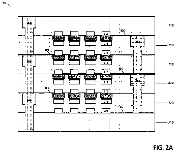
cooling
channels formed by concave regions of the HTS material and/or conductive
material
within the conducting channel.
[0005] The foregoing apparatus and method embodiments may be
implemented
with any suitable combination of aspects, features, and acts described above
or in further
detail below. These and other aspects, embodiments, and features of the
present
- 1 -
CA 03167302 2022- 8-8
WO 2021/195383
PCT/US2021/024160
teachings can be more fully understood from the following description in
conjunction
with the accompanying drawings.
BRIEF DESCRIPTION OF DRAWINGS
[0006] Various aspects and embodiments will be described with
reference to the
following figures. It should be appreciated that the figures are not
necessarily drawn to
scale. In the drawings, each identical or nearly identical component that is
illustrated in
various figures is represented by a like numeral. For purposes of clarity, not
every
component may be labeled in every drawing.
[0007] FIG. 1 is a cross-sectional view of a portion of an
illustrative plate suitable
for use in a stacked-plate superconducting magnet, according to some
embodiments;
[0008] FIGs. 2A-2B show different cross-sections of an
illustrative stack of plates
in a superconducting magnet, according to some embodiments;
[0009] EEGs 3A-3B are perspective views of opposing surfaces
of an illustrative
individual plate of a type which may be included in a stack of plates in a
superconducting magnet, according to some embodiments;
[0010] FIGs. 3C-3D are perspective views of opposing surfaces
of an illustrative
individual plate of a type which may be included in a stack of plates in a
superconducting magnet, according to some embodiments;
[0011] FIG. 4 is a perspective view of an illustrative stack
of plates of a
superconducting magnet, according to some embodiments;
[0012] FIG. 5 is a perspective view of an illustrative stack
of plates of a
superconducting magnet with an exterior case, according to some embodiments;
[0013] FIG. 6 depicts a cross-sectional view of a stack of
plates depicting the
structural load on the stack, according to some embodiments;
[0014] FIG. 7 illustrates an example of a plate in which HTS
material is provided
as a stack of HTS tape, according to some embodiments,
[0015] FIG. 8 illustrates an example of a plate in which the
conducting channels
comprise a stack of co-wound HTS tapes in addition to conductive co-wound
tape,
according to some embodiments;
[0016] FIGs. 9A-9C depict cross-sections of illustrative
plates suitable for use in a
stacked-plate superconducting magnet in which the cooling channels are
arranged within
the conducting channels, according to some embodiments;
- 2 -
CA 03167302 2022- 8-8
WO 2021/195383
PCT/US2021/024160
[0017] FIG. 10 is a three-dimensional graphic of a fusion
power plant with a
cutaway portion illustrating various components of the power plant, according
to some
embodiments; and
[0018] FIGs. 11A-11B depicts aerial views of illustrative
cooling channel
arrangements, according to some embodiments.
DETAILED DESCRIPTION
[0019] A high-field superconducting magnet often comprises
multiple electrically
insulated cable turns grouped in a multi-layer arrangement. When the
superconducting
material is cold enough to be below its critical temperature (the temperature
below which
the electrical resistivity of the material drops to zero), driving the magnet
allows current
to pass through the superconducting path without losses. However, for various
reasons
some or all of the superconducting material may be heated to above its
critical
temperature and therefore lose its superconducting characteristics If
uncontrolled, such
heating can lead to the superconductor losing its superconducting abilities,
often referred
to as a "quench." Moreover, if the quench is not properly addressed by the
system (e.g.,
by shutting down), components can be damaged by the heating.
[0020] Some superconducting magnet systems handle quench
events via a system
of active alarms and detection mechanisms. Other superconducting magnet
systems
handle quenches passively through design of the superconducting magnet itself
An
example of the latter approach is a non-insulated (Ni) magnet (also referred
to as a no-
insulation (NI) magnet), in which adjacent superconducting turns of the magnet
are not
insulated from one another but are instead separated by a conventional
conductor (i.e.,
not a superconductor). When the magnet is operating below the superconductor's
critical
temperature, current flows through the superconductor and not across turns
because the
superconductor has zero resistance compared with the finite resistance of the
conductor
that lies between the turns.
[0021] During a quench, however, at least one or more
portions of the
superconductor may be in a "normal" (non-superconducting) state (i.e., at
least one or
more portions of the superconductor have a finite resistance rather than a
zero resistance
which is characteristic of a superconductor). The at least one or more
portions of the
superconductor having a normal resistance are sometimes referred to as "normal
zones"
- 3 -
CA 03167302 2022- 8-8
WO 2021/195383
PCT/US2021/024160
of the superconductor. When normal zones appear, at least some zero resistance
current
pathways are no longer present, causing the current to flow through the normal
zones
and/or between the turns, with the balance of current flow between these
pathways
depending on their relative resistances. By diverting at least some current
from the
superconducting material when it is normal in this manner, therefore, NI
magnets, and in
particular non-insulated high temperature superconductor (N I-HT S) magnets
(NI
magnets that comprise HTS), can in principle be passively protected against
quench
damage without the need to continuously monitor quench events and/or to
actively
engage external quench protection mechanisms.
[0022] The inventors have recognized and appreciated a non-
insulated
superconducting magnet design that comprises a stack of conductive plates that
each
include a spiral groove. A superconductor can be arranged within the grooves
and the
plates stacked such that the superconductor forms a continuous current path
through the
plates, making a spiral path within each plate. The conductive plates act as
the
conductive material that is arranged between the turns of the superconducting
magnet in
the NI design discussed above. The spiral-grooved, stacked-plate design has
the
advantage that it is scalable to large bore magnets, and can be configured to
have a high
overall current density, be thermally stable, and mechanically stable.
[0023] As the size of NI magnets constructed using the spiral-
grooved, stacked-
plate design increase, however, there is a concomitant increase of the Lorentz
loads on
various regions of the conductor. Such increased Lorentz loads may lead to
reduced
structural integrity of the NI magnet. Moreover, the amount of internal
volumetric
heating may also increase as the magnets become larger. These conditions
thereby
require further consideration as to how cooling and conductive paths are
arranged within
a spiral-grooved, stacked-plate NI magnet design.
[0024] The inventors have recognized and appreciated schemes
for conductor and
coolant placement in stacked-plate superconducting magnets. In particular, the
inventors
have recognized that there are advantages to arranging coolant channels and
conducting
channels within the plates on opposing faces. If the two types of channels are
aligned
with one another across the plate stacks, the plates may be stacked such that
the cooling
channel in one plate is adjacent to the conducting channel of the neighboring
plate. By
stacking a number of these plates, therefore, cooling may be supplied to each
conducting
- 4 -
CA 03167302 2022- 8-8
WO 2021/195383
PCT/US2021/024160
channel through the cooling channels of each neighboring plate. Moreover, by
aligning
the two types of channels, the stacks of plates may have improved mechanical
strength
because mechanical load paths may be created through the entire stack that do
not pass
through any of the channels. If the plates are also formed from (e.g., via
traditional
machining processes, via additive and/or subtractive processes, etc.) an
appropriately
strong material, this arrangement of channels may produce a very strong stack
of plates
that can withstand high Lorentz loads.
[0025] One benefit of this design is that cryogenic coolant
may make direct contact
with material in the conducting channel (which may be, or may include, the
superconducting material) along a substantial length of the conducting
channel, because
the two types of channel are aligned as such. Very efficient cooling can
therefore be
delivered to the superconducting material in the magnet. Moreover, no
dedicated
cooling plates are needed, because all of the cooling necessary may be
included within
the same plates that house the superconductors
[0026] According to some embodiments, the conducting channels
of the plates may
comprise an HTS superconductor electrically coupled to a second conductor,
such as
copper. The second conductor may be aligned with the opening of the conducting
channel ¨ for instance, the second conductor may have a surface that is flush
with the
face of the plate in which the conducting channel is arranged. In this case,
the TITS
superconductor is embedded within the channel beneath the second conductor. In
some
embodiments, the conducting channels may comprise a third conductor, such as a
Pb or
Sn solder, which fills the space in the channel other than the second
conductor and the
HTS superconductor. In some cases, the third conductor may electrically couple
the
HTS superconductor to the second conductor.
[0027] According to some embodiments, a stacked-plate
superconducting magnet
may comprise alternating types of plates within the bulk of the stack of
plates. For
instance, a first type of plate may include conducting channels that spiral
inward, while a
second type of plate may include conducting channels that spiral outward. By
arranging
suitable connection points between the plates, a continuous conductive path
through all
of the conducting channels may be arranged, while providing cooling throughout
the
stack of plates. Such a design may also lead to being particularly modular,
since aside
from possibly the uppermost and/or lowermost plate (e.g., terminal plates),
the bulk of
- 5 -
CA 03167302 2022- 8-8
WO 2021/195383
PCT/US2021/024160
the stack of plates may be formed or arranged by alternating placement of the
two types
of plates.
[0028] According to some embodiments, the conducting channel
in a stacked-plate
superconducting magnet may be arranged in a racetrack spiral (or simply
"racetrack
pattern"). In a racetrack spiral, the path follows a racetrack shape (e.g., a
rectangle with
rounded corners) without spiraling inward or outward for most of the
circumference, but
includes a number of "jogs" or "joggles" in which the path jogs inward or
outward.
These jogs cause the racetrack spiral to wind inward or outward, depending on
the
direction of the jogs.
[0029] According to some embodiments, electrically insulating
material may be
arranged between plates of the stack of plates. In some cases, the insulation
may cover
part of, but not all, of the face of the plate. Conducting pads electrically
connecting
neighboring plates may, for instance, not have intervening insulating material
between
the pads. Moreover, at least some portion of the surface area of neighboring
plates may
contact one another directly, with the majority of the surface area of the
contact between
the plates being via insulating material. Arranging insulating material in
this way may
provide a conductive path between plates of the stack while maximizing the
length of the
conductive path, which may provide beneficial properties during magnet
charging and
during a quench.
[0030] Following below are more detailed descriptions of
various concepts related
to, and embodiments of, schemes for conductor and coolant placement in stacked-
plate
superconducting magnets. It should be appreciated that various aspects
described herein
may be implemented in any of numerous ways. Examples of specific
implementations
are provided herein for illustrative purposes only. In addition, the various
aspects
described in the embodiments below may be used alone or in any combination,
and are
not limited to the combinations explicitly described herein.
[0031] FIG. 1 is a cross-section of a portion of an
illustrative plate suitable for use
in a stacked-plate superconducting magnet, according to some embodiments. In
the
example of FIG. 1, plate 100 comprises a baseplate material 110, in which are
formed
(e g , via traditional machining processes, via additive and/or subtractive
processes, etc.)
cooling channels 112 and conducting channels 114. In the conducting channels
are
arranged an HTS material 122, a cap 126 and an intervening conductive material
124
- 6 -
CA 03167302 2022- 8-8
WO 2021/195383
PCT/US2021/024160
which provides electrical and thermal contact between the HTS material 122 and
cap
126.
[0032] It will be appreciated that another portion of plate
100 not shown in FIG 1
may comprise a "jog" region in which the path of the conductive channel jog
outward or
inward to move to the next outer or inner racetrack path, respectively. For
instance, in
the case where the cross-section shown in FIG. 1 represents a portion of a
plate in which
the conductive channels 114 spiral inward, another portion of the plate may
include an
inward jog for at least some of the channels to connect the channel to the
next innermost
channel (e.g., outermost channel to 2nd outermost channel, etc.).
[0033] According to some embodiments, cooling channels 112
are open channels
within the plate 100. The cooling channels may become closed, thereby allowing
cryogens to flow through the channels, by arranging the plate 100 adjacent to
another
plate, such as another instance of plate 100. For example, when two instances
of the
plate 100 are stacked on top of one another, the cooling channels 112 may
contact the
caps 126 around the edges of each cooling channel. As a result, the cryogen
flowing
through the cooling channel may be in direct contact with the cap 126.
[0034] According to some embodiments, the baseplate 110 may
comprise, or may
consist of, a high mechanical strength material such as but not limited to
steel, Inconel ,
Nitronic 40, Nitronic 50, Incoloy , or combinations thereof In some
embodiments,
the baseplate 110 may be plated with a metal such as nickel to facilitate
adhesion of
other components to the plate, including solder as described below.
[0035] According to some embodiments, the HTS 122 may
comprise a rare earth
barium copper oxide superconductor (REBCO), such as yttrium barium copper
oxide
(YBCO). In some embodiments, the HTS 122 may comprise a co-wound stack of HTS
tape. In embodiments, the HTS tape may comprise a long, thin strand of HTS
material
with cross-sectional dimensions in the range of about 0.001 mm to about 0.1 mm
in
thickness (or height) and a width in the range of about 1 mm to about 12 mm
(and with a
length that extends along the length of the cable, e.g., into and out of the
page in the
example of FIG. 1). According to some embodiments, each strand of HTS tape may
comprise an HTS material such as REBCO in addition to an electrically
conductive
material. In some embodiments, the electrically conductive material may be
disposed
on the REBCO. In some embodiments, the electrically conductive material may be
a
- 7 -
CA 03167302 2022- 8-8
WO 2021/195383
PCT/US2021/024160
cladding material such as copper. In some embodiments, HTS tape may comprise a
polycrystalline HTS and/or may have a high level of grain alignment.
[0036] According to some embodiments, cap 126 may comprise,
or may consist of,
copper. It may be noted that, as a result of the plate 100 being shown in
cross-section in
FIG. 1, that the shapes of the HTS 122 in the plate 100, and of the cap 126 in
the plate
100, are generally that of a spiral (e.g., a racetrack spiral).
[0037] According to some embodiments, conductive material 124
may comprise a
Pb and/or Sn solder. In some embodiments, conductive material 124 may comprise
a
metal having a melting point of less than 200 C, wherein at least 50 wt% of
the metal is
Pb and/or Sn, and at least 0.1 wt% of the metal is Cu.
[0038] As shown in FIG. 1, the cap 126 is arranged within an
upper section of
channels 114 that is wider than the lower section in which the HTS 122 and
conductive
material 124 are located. In some embodiments, the conductive material 124 may
be
introduced into the plate 100 as a molten solder subsequent to arranging the
HTS 122
and cap 126 within the conducting channel 114. As a result, the conductive
material 124
may fill the space between the HTS 122 and cap 126 and/or may fill any space
around
the sides of the HTS 122 and/or cap 126, should such space be present prior to
filling or
otherwise occupying the space with the solder.
[0039] In some embodiments, the HTS 122 may be pre-tinned
with a metal (e.g., a
PbSn solder) to promote a good bond between the HTS 122 and the solder.
According to
some embodiments, the conductive material 124 may be deposited via a vacuum
pressure
impregnation (VPI) process. Such a process may comprise one or more of the
following
steps: cleaning the empty space within the cable using an acidic solution
following by a
water rinse; evacuating the space within the cable; purging the space with an
inert gas;
depositing flux into the space to coat the HTS 122 and the conductive material
124;
draining any excess flux from the cable; heating the cable to a temperature
below, at, or
above a temperature at which the alloy to be deposited will melt; and flowing
a molten
alloy (e.g., a PbSn solder) into the plate.
[0040] According to some embodiments, plate 100 may comprise
one or more
through holes (not shown in FIG. 1) for attaching the plate to other plates
and/or other
- 8 -
CA 03167302 2022- 8-8
WO 2021/195383
PCT/US2021/024160
structures. In some cases, the through holes may comprise an interior thread
to facilitate
insertion of mechanical fasteners such as screws or bolts into or through the
plate.
[0041] In the example of FIG. 1, it will be appreciated that
while particular shapes
of the channels 112 and 114 are illustrated, the techniques described herein
are not
limited to channels with these particular shapes. For instance, the channels
could have a
half-circle cross-section instead of the rectangular cross-section shown, or
another other
suitable shape cross-section.
[0042] FIGs. 2A-2B show different cross-sections of an
illustrative stack of plates
in a superconducting magnet, according to some embodiments. Stack of plates
200
comprises two instances of plate 210 and two instances of plate 220, in
addition to
terminal plates 230 and 240. Layers of insulating material 250 are arranged at
selected
regions between neighboring plates. FIG. 2A represents a cross-section of the
stack of
plates through the racetrack portion of the channels of the plates, whereas
FIG. 2B
represents a cross-section of the stack of plates in the region in which the
conducting
channels "jog" in or out to switch lanes of the racetrack spiral.
[0043] As noted above in relation to FIG. 1, the open cooling
channels in one plate
may be arranged adjacent to the conducting channel of the neighboring plate.
For
example, as shown in FIG. 2A, which represents the racetrack portion of the
channels,
the cooling channels 211 in each instance of plate 210 are arranged adjacent
to the cap
226 of the neighboring plate 220. Similarly, the cooling channels 221 in plate
220 are
arranged adjacent to the cap 216, with cooling channels 231 arranged in the
terminal cap
230 arranged adjacent to the uppermost instance of the plate 210.
[0044] It may be noted that cooling channels 221 in the
lowermost instance of plate
220 are not strictly needed since there are no conductors adjacent to these
channels.
However, due to the modular nature of the plates in the stack 200, it may be
more
convenient to simply use an instance of plate 220 rather than fabricate a new
type of
plate that does not include the lowermost cooling channels 221.
[0045] In the example of FIGs. 2A-2B, the plates 210, 220,
230 and 240 are held
together, at least in part, by bolts 280, which connect neighboring pairs of
plates as
shown in FIG. 2A. It may be presumed that such bolts are present at a number
of
- 9 -
CA 03167302 2022- 8-8
WO 2021/195383
PCT/US2021/024160
locations around the plates 210, 220, 230 and 240, although the cross-section
shown in
FIG. 2B does not include any such bolts for clarity.
[0046] As shown in FIG. 2B, the plates may include conductive
pads to connect
the conductive paths in one plate to those of an adjacent plate. For example,
the terminal
plate 230 includes pad 239 which is adjacent to and electrically connected to
the
conductor 216 in the conducting channel of plate 210. Thus, the terminal plate
may be
adjacent to and electrically connected to one end of the conductive channel of
plate 210,
the other end of which is electrically connected to the pad 219. Pad 219 is,
in turn,
adjacent to and electrically connected to, the conductor 226 in the conducting
channel of
plate 220. The other end of the conductor 226 in the conducting channel of
plate 220 is
adjacent to and electrically connected to pad 229, which is adjacent to and
electrically
connected to the next plate 210, and so forth. In the example of FIG. 2B, the
conductive
pads 219, 229, 239 and 249 are shaded in the same manner as the caps of the
plates,
although it will be appreciated that in general the pads and caps need not
comprise the
same material(s).
[0047] According to some embodiments, insulating material 250
may comprise
polyimide (e.g., Kapton8), epoxy resin, phenolic resin, glass epoxy laminate,
a plastic,
an elastomer, or combinations thereof According to some embodiments,
insulating
material may have a breakdown voltage or dielectric strength of greater than
25 kV/mm,
of greater than 50 kV/mm, of greater than 75 kV/mm, of greater than 100 kV/mm.
In
some cases, the voltages in the superconducting magnet may be comparatively
low, in
which case a low voltage standoff insulating material such as anodized
aluminum could
be utilized as the insulating material 250.
[0048] According to some embodiments, the baseplates 210a,
220a, 230a and 240a
may each comprise, or may consist of, a high mechanical strength material such
as but
not limited to steel, Inconel , Nitronic 40, Nitronic 50, Incoloye, or
combinations
thereof In some embodiments, the baseplates 210a, 220a, 230a and 240a may be
plated
with a metal such as nickel to facilitate adhesion of other components of the
plate,
including solder.
[0049] In the example of FIGs. 2A, bolts 290 are arranged
within through holes of
the plates 210, 220, 230 and 240 and affix neighboring pairs of plates to one
another.
- 10 -
CA 03167302 2022- 8-8
WO 2021/195383
PCT/US2021/024160
[0050] To further illustrate the structure of a stack of
plates such as those shown in
FIGs. 2A-2B, FIGs. 3A-3D depict upper and lower views of individual plates 210
and
220.
[0051] FIGs. 3A and 3B depict upper and lower views,
respectively, of plate 210,
wherein the cross-section of FIG. 2A is through the section marked A-A! and
the cross-
section of FIG. 2B is through the section marked B-B'. In the example of FIGs.
3A-3B,
the location of cooling channels 221, which are part of plate 220 arranged
above the
plate 210, are shown for purposes of explanation, although it will be
appreciated that
these cooling channels are not in fact part of the plate 210. As may be noted,
the
conducting channel of plate 210 in this example has an inward spiral when
following the
channel in a clockwise direction viewed from above.
[0052] As may be seen in FIG. 3A, for the bulk of the
racetrack sections of the
conducting channel of the plate 210 ¨ of which the cap 216 is visible ¨ the
cooling
channels 221 of the neighboring plate 220 are aligned with the conducting
channel. As
such, cryogen passing through the cooling channels may directly contact the
cap 216 and
deliver cooling to the HTS material arranged beneath the cap as discussed
above.
[0053] The region of the plate 210 between the coolant inlet
and outlet (the two
regions where the coolant channels meet the edge of the plate) includes, in
the example
of FIG. 3A, a "meandering" region of the cooling channel 221 that meanders
back and
forth over the conducting channels 216. Various other arrangements may be
envisioned,
including a cooling channel that is aligned with a single conducting channel,
but runs
back and forth over successive cooling channels in the region between the
inlet and
outlet.
[0054] In some embodiments, the inlet and outlet regions of
the plate may be
further apart than is shown in the example of FIG. 3A, such as at opposite
ends of the
plate from one another. In such cases, the cooling channels may be arranged so
that
some cooling channels (e.g., half) pass along one side of the plate with the
other cooling
channels passing along the other side of the plate. An example of such a
cooling channel
configuration is depicted in FIG. 11A, which shows a single layer of cooling
channels
1111 in an aerial view. FIG 11B depicts the cooling channels 221 of the layer
of the
plate shown in FIG. 3A with the same aerial view for comparison. It may be
noted that
alternative cooling channel arrangements such as that shown in FIG. 11A may be
- 11 -
CA 03167302 2022- 8-8
WO 2021/195383
PCT/US2021/024160
arranged on a plate without altering the structure of the other elements of
the plate except
for the portion(s) of the baseplate that connect the cooling channels to the
edge of the
plate. For instance, as shown in FIG. 3A the cooling channels may be arranged
as shown
in FIG. 11A without altering the conductive channels of the plate.
[0055] FIG. 3B illustrates the underside of plate 210, and
includes portions to
which insulating material 250 is attached, and portions for which the
baseplate 210a is
exposed.
[0056] FIGs. 3C and 3D depict upper and lower views,
respectively, of plate 220,
wherein the cross-section of FIG. 2A is through the section marked A-A' and
the cross-
section of FIG. 2B is through the section marked B-B'. In the example of FIGs.
3C-3D,
the location of cooling channels 211, which are part of plate 210 arranged
above the
plate 220, are shown for purposes of explanation, although it will be
appreciated that
these cooling channels are not in fact part of the plate 220. As may be noted,
the
conducting channel of plate 220 in this example has an outward spiral when
following
the channel in a clockwise direction viewed from above.
[0057] As may be seen in FIG. 3C, for the bulk of the
racetrack sections of the
conducting channel of the plate 220 ¨ of which the cap 226 is visible ¨ the
cooling
channels 211 of the neighboring plate 210 are aligned with the conducting
channel. As
such, cryogen passing through the cooling channels may directly contact the
cap 226 and
deliver cooling to the HTS material arranged beneath the cap as discussed
above.
[0058] The region of the plate 220 between the coolant inlet
and outlet (the two
regions where the coolant channels meet the edge of the plate) includes, in
the example
of FIG. 3C, a "meandering- region of the cooling channel 211 that meanders
back and
forth over the conducting channels 226. Various other arrangements may be
envisioned,
including a cooling channel that is aligned with a single conducting channel,
but runs
back and forth over successive cooling channels in the region between the
inlet and
outlet.
[0059] In some embodiments, the inlet and outlet regions of
the plate may be
further apart than is shown in the example of FIG. 3C, such as at opposite
ends of the
plate from one another. In such cases, the cooling channels may be arranged so
that
- 12 -
CA 03167302 2022- 8-8
WO 2021/195383
PCT/US2021/024160
some cooling channels (e.g., half) pass along one side of the plate with the
other cooling
channels passing along the other side of the plate.
[0060] FIG. 3D illustrates the underside of plate 220, and
includes portions to
which insulating material 250 is attached, and portions for which the
baseplate 220a is
exposed.
[0061] FIG. 4 is a perspective view of an illustrative stack
of plates of a
superconducting magnet, according to some embodiments. Stack of plates 400
represents an exterior perspective view of the stack of plates shown in cross-
section in
FIGs. 2A-2B. As in FIGs. 3A-3D, the cross-section of FIG. 2A is through the
section
marked A-A and the cross-section of FIG. 2B is through the section marked B-
B'.
[0062] As shown in the example of FIG. 4, the terminal plates
at the top and the
bottom of the stack each comprise a conductive portion 438 and 448,
respectively, that
extends outward from the stack and that are electrically connected to one
another through
the spiral conducting paths within the stack. Each cooling channel of the
plates of the
stack terminates at a common set of ports 470 at one end of the channel and at
a common
set of ports 480 at the other end of the channel. Since the ends of the
cooling channels
are arranged together, with all the inlets together and all the outlets
together, a single
large inlet or outlet port may be formed (e.g., via traditional machining
processes, via
additive and/or subtractive processes, etc.) around the set of channels at
each end, as
shown in FIG. 5. This may allow coolant to pass through all the cooling
channels of the
stack of plates using just a single inlet pipe and a single outlet pipe.
[0063] FIG. 5 is a perspective view of an illustrative stack
of plates of a
superconducting magnet with an exterior case, according to some embodiments.
Subsequent to assembly of the stack of plates, some or all of the exterior of
the stack
may have an insulating material disposed thereon (e.g. some or all of the
exterior of the
stack may be wrapped in an insulating material). In the example of FIG. 5, the
entire
stack of plates except for the cooling inlet and outlet 570 and 580, and the
ends of the
terminal plates that include conductive portions 528 and 548, are wrapped in
an
insulating material 550 such as polyimide (e.g., Kaptone), epoxy resin,
phenolic resin,
glass epoxy laminate, a plastic, an elastomer, or combinations thereof
According to
some embodiments, the insulating material 550 may have a breakdown voltage or
dielectric strength of greater than 25 kV/mm, of greater than 50 kV/mm, of
greater than
- 13 -
CA 03167302 2022- 8-8
WO 2021/195383
PCT/US2021/024160
75 kV/mm, of greater than 100 kV/mm. In some cases, the voltages in the
superconducting magnet may be comparatively low, in which case a low voltage
standoff
insulating material such as anodized aluminum could be utilized as the
insulating
material 550.
[0064] Subsequent to application of the insulating material
550, the stack of plates
are enclosed within a case 590, which provides further structural stability to
the stack of
plates and may comprise fiberglass, for instance. In some cases, the case 590
may
comprise a high mechanical strength material such as but not limited to steel,
Inconel ,
Nitronic 40, Nitronic 50, Incoloy , or combinations thereof. In some
embodiments,
any gaps between the stack of plates and the case 590 may be filled with an
insulating
material such as epoxy resin.
[0065] As discussed above, alignment of the cooling channels
and the conducting
channels across the plates provides structural benefits, as illustrated in
FIG. 6, which
depicts a cross-sectional view of a stack of plates similar to that shown in
FIG. 2A to
depict the structural load on such a stack.
[0066] As shown in FIG. 6, in zones where the cooling
channels and the
conducting channels are aligned along the thickness dimension of the stack
(the
dimensional along which the plates are stacked on top of one another), the
high-strength
material in the baseplates 610a, 620a, 630a and 640a makes direct contact
through the
thin insulating material 650. This effectively forms a strong structural
'cage' that
surrounds the conductors, shunting the load path around them. As a result, the
primary
load path passes between the conducting channels and the cooling channels, as
shown by
the vertical dashed arrows.
[0067] Furthermore, out-of-plane IxB body loads from the
individual HTS/cap
stacks are transferred to this structure, minimizing accumulation of
compressive loads on
the HTS/cap composite. Similarly, external out-of-plane compressive loads are
shunted
around the conductors via the cage structure.
[0068] As discussed above in relation to FIG. 1, the HTS
material 122 shown in
FIG. 1 may comprise a co-wound stack of HTS tapes. FIG. 7 illustrates an
example of
plate 100 of FIG. 1 in which the HTS material is provided as a stack of HTS
tapes 722.
In FIG. 7, the plate 700 comprises a baseplate material 710, cooling channels
712,
- 14 -
CA 03167302 2022- 8-8
WO 2021/195383
PCT/US2021/024160
conductive material 724 and caps 726. HTS tape may comprise a long, thin
strand of
HTS material with cross-sectional dimensions in the range of about 0.001 mm to
about
0.1 mm in thickness (or height) and a width in the range of about 1 mm to
about 12 mm
(and with a length that extends along the length of the cable, i.e., into and
out of the page
in the example of FIG. 7). According to some embodiments, HTS tapes 722 may
comprise an HIS material in addition to cladding materials such as copper. In
some
embodiments, HTS tape may comprise a polycrystalline HTS and/or may have a
high
level of grain alignment.
[0069] In some situations in which the HTS material is
provided as an HTS tape, it
may be desirable to vary the number of HTS conductors in a stack of co-wound
HTS
tapes according to their location within the magnet, thereby reducing the
total amount of
HTS tape needed to construct the magnet. FIG. 8 illustrates an example of
plate 100 of
FIG. 1 in which the conducting channels 814 comprise a stack of co-wound HTS
tapes
822 in addition to conductive co-wound tape 823 (e.g., copper tape) As may be
noted
from FIG. 8, the number of HTS tapes is decreased in each turn going from
right to left
in FIG. 8, while the number of conductive co-wound tapes is increased right-to
left. The
width of the cap 826 is varied in conjunction with number of conductive co-
wound tapes
such that their combined cross-sectional area is roughly constant in every
turn. In this
way, the resistance per unit length of the co-conductor is maintained constant
throughout
the winding pack.
10070] Tuning the amount of HTS tape 822, co-wound conductive
tape 823, and
the size of the cap 826 may provide a way to control the rate of magnetic
energy
dissipation during a quench, and in some cases may dissipate the magnetic
energy
uniformly throughout the winding pack during a full magnet quench event. In
addition,
tuning the amount of HTS tape 822, co-wound conductive tape 823, and the size
of the
cap 826 may alter an amount of magnetic energy deposition in adjacent areas.
This may
allow, for instance, reduction of the magnetic energy deposition in critical
areas such as
in regions with joints.
10071] While in each of the examples discussed above, the
cooling channels are
arranged on the opposite side of a plate from the conducting channels, in some
cases it
may be preferable to provide the cooling channels within the conducting
channels. FIG.
9A is a cross-section of a portion of an illustrative plate suitable for use
in a stacked-
- 15 -
CA 03167302 2022- 8-8
WO 2021/195383
PCT/US2021/024160
plate superconducting magnet in which the cooling channels are arranged within
the
conducting channels, according to some embodiments.
[0072] As shown in FIG 9A, the conducting channels 914 also
comprise the
cooling channels 912, which are formed (e.g., via traditional machining
processes, via
additive and/or subtractive processes, etc.) by appropriate shaping of the
caps 926
(although any portion of the conducting channel could be shaped as desired in
general).
The co-linear conducting channels 914 and cooling channels 912 are arranged
within the
baseplate 910. While in the example of FIG. 9A the conductive material 926
have the
cooling channels provided therein, it will be appreciated that cooling
channels could be
in general formed (e.g., via traditional machining processes, via additive
and/or
subtractive processes, etc.) in the conductive material and/or HTS 922,
depending on the
geometrical arrangement of the conductive material and HTS within the
conductive
channel, since the cooling channels may be formed or provided from at least
portions of
concave regions of the upper portion of the material within the conductive
channel
[0073] In the example of FIG. 9A, the plate 900 can thereby
be stacked on top of
multiple instances of itself to produce a stack of plates in which the cooling
channels are
adjacent to the conducting channels. This stacking may be performed in two
different
ways, which are depicted in FIGs. 9B and 9C.
[0074] As shown in FIG. 9B, a magnet 950 may comprise two
instances of the
plate 900 stacked on top of one another, wherein a planar face of one of the
plates rests
over the cooling channels, thereby bounding the cooling channels. As a result,
when
coolant is passed through the magnet 950, it may contact the conductive
material 926 in
one plate and the baseplate material in the adjacent plate. An insulating
layer 950 may
be arranged between the baseplates 910.
[0075] Alternatively, as shown in FIG. 9C, a magnet 960 may
comprise two
instances of the plate 900 stacked on top of one another wherein the
orientation of one
plate 900 is flipped so that the cooling channels contact one another and are
aligned,
forming cooling channels 935, which are actually a combination of the cooling
channels
912 formed in each of the two plates and aligned so that their surfaces bound
one
another. An insulating layer 950 may be arranged between the baseplates 910_
It will be
appreciated that some or all of insulating layer 950 in FIG. 9C may comprise
air as an
insulator. For instance, the illustrated layer may not extend all the way to
the cooling
- 16 -
CA 03167302 2022- 8-8
WO 2021/195383
PCT/US2021/024160
channels 935 as shown, with a small air gap left between the two layers of
conductive
material 926 adjacent to the cooling channels.
[0076] FIG. 10 is a three-dimensional graphic of a fusion
power plant with a
cutaway portion illustrating various components of the power plant, according
to some
embodiments. A magnet within a fusion power plant may be formed from
superconductor arrangement as described above. FIG. 10 shows a cross-section
through
a power plant and includes a magnet coil 1014, which is fabricated from, or
otherwise
includes, a superconducting magnet comprising a stack of plates as discussed
and
described above, a neutron shield 1012, and a core region 1011. According to
some
embodiments, the magnet coil 1014 may be, or may form part of, a toroidal
field coil.
Magnet coil 1013 may be fabricated from, or otherwise includes, a
superconducting
magnet comprising a stack of plates as discussed and described above.
According to
some embodiments, the magnet coil 1013 may be, or may form part of a central
solenoid
and/or other poloidal field solenoidal coils
[0077] Persons having ordinary skill in the art may
appreciate other embodiments
of the concepts, results, and techniques disclosed herein. It is appreciated
that
superconducting cables configured according to the concepts and techniques
described
herein may be useful for a wide variety of applications, including
applications in which
the superconducting cable is wound into a coil to form a magnet. For instance,
one such
application is conducting nuclear magnetic resonance (NMR) research into, for
example,
solid state physics, physiology, or proteins, for which such cables may be
wound into a
magnet. Another application is performing clinical magnetic resonance imaging
(MRI)
for medical scanning of an organism or a portion thereof, for which compact,
high-field
magnets are needed. Yet another application is high-field MRI, for which large
bore
solenoids are required. Still another application is for performing magnetic
research in
physics, chemistry, and materials science. Further applications is in magnets
for particle
accelerators for materials processing or interrogation; electrical power
generators;
medical accelerators for proton therapy, radiation therapy, and radiation
generation
generally; superconducting energy storage; magnetohydrodynamic (MHD)
electrical
generators; and material separation, such as mining, semiconductor
fabrication, and
recycling. It is appreciated that the above list of applications is not
exhaustive, and there
- 17 -
CA 03167302 2022- 8-8
WO 2021/195383
PCT/US2021/024160
are further applications to which the concepts, processes, and techniques
disclosed herein
may be put without deviating from their scope.
[0078] As used herein, a "high temperature superconductor" or
"HTS" refers to a
material that has a critical temperature above 30 K, wherein the critical
temperature
refers to the temperature below which the electrical resistivity of the
material drops to
zero.
[0079] Illustrative examples of conducting channels and
cooling channels are
described herein and illustrated in the drawings. It will be appreciated that
the particular
size and shape of these channels are provided merely as examples and that no
particular
cross-sectional shape or size is implied as being necessary or desirable
unless otherwise
noted.
100801 Having thus described several aspects of at least one
embodiment which
illustrate the described concepts, it is to be appreciated that various
alterations,
modifications, and improvements will readily occur to those skilled in the
art.
[0081] Such alterations, modifications, and improvements are
intended to be part
of this disclosure, and are intended to be within the spirit and scope of the
concepts
described herein. Further, though advantages of the concepts described herein
are
indicated, it should be appreciated that not every embodiment of the
technology
described herein will include every described advantage. Some embodiments may
not
implement any features described as advantageous herein and in some instances
one or
more of the described features may be implemented to achieve further
embodiments.
Accordingly, the foregoing description and drawings are by way of example
only.
[0082] Various aspects of the concepts described herein may
be used alone, in
combination, or in a variety of arrangements not specifically discussed in the
embodiments described in the foregoing and is therefore not limited in its
application to
the details and arrangement of components set forth in the foregoing
description or
illustrated in the drawings. For example, aspects described in one embodiment
may be
combined in any manner with aspects described in other embodiments.
[0083] Also, the concepts described herein may be embodied as
a method, of
which an example has been provided. The acts performed as part of the method
may be
ordered in any suitable way. Accordingly, embodiments may be constructed in
which
- 18 -
CA 03167302 2022- 8-8
WO 2021/195383
PCT/US2021/024160
acts are performed in an order different than illustrated, which may include
performing
some acts simultaneously, even though shown as sequential acts in illustrative
embodiments.
[0084] Further, some actions are described as taken by a
"user." It should be
appreciated that a "user" need not be a single individual, and that in some
embodiments,
actions attributable to a "user- may be performed by a team of individuals
and/or an
individual in combination with computer-assisted tools or other mechanisms.
[0085] Use of ordinal terms such as "first," "second,"
"third," etc., in the claims to
modify a claim element does not by itself connote any priority, precedence, or
order of
one claim element over another or the temporal order in which acts of a method
are
performed, but are used merely as labels to distinguish one claim element
having a
certain name from another element having a same name (but for use of the
ordinal term)
to distinguish the claim elements.
[0086] The terms "approximately" and "about" may be used to
mean within 20%
of a target value in some embodiments, within 10% of a target value in some
embodiments, within +5% of a target value in some embodiments, and yet within
+2% of
a target value in some embodiments. The terms "approximately" and "about" may
include the target value The term 'substantially equal" may be used to refer
to values
that are within +20% of one another in some embodiments, within 10% of one
another
in some embodiments, within +5% of one another in some embodiments, and yet
within
2% of one another in some embodiments
[0087] The term "substantially" may be used to refer to
values that are within
+20% of a comparative measure in some embodiments, within +10% in some
embodiments, within +5% in some embodiments, and yet within +2% in some
embodiments. For example, a first direction that is "substantially"
perpendicular to a
second direction may refer to a first direction that is within 20% of making
a 90 angle
with the second direction in some embodiments, within 10% of making a 90
angle
with the second direction in some embodiments, within +5% of making a 90
angle with
the second direction in some embodiments, and yet within 2% of making a 90
angle
with the second direction in some embodiments
- 19 -
CA 03167302 2022- 8-8
WO 2021/195383
PCT/US2021/024160
[0088] Also, the phraseology and terminology used herein is
for the purpose of
description and should not be regarded as limiting. The use of "including,"
"comprising," or "having," "containing," "involving," and variations thereof
herein, is
meant to encompass the items listed thereafter and equivalents thereof as well
as
additional items.
- 20 -
CA 03167302 2022- 8-8