Note : Les descriptions sont présentées dans la langue officielle dans laquelle elles ont été soumises.
1
TOOL FOR TESTING AN ELECTRON-OPTICAL ASSEMBLY
FIELD
[0001] The embodiments provided herein generally relate to a tool for testing
an electron-optical
assembly.
[0002] An electron-optical assembly is configured to manipulate one or more
beams of charged
particles, such as by deflecting and/or focusing the beams of charged
particles. Embodiments provide
a tool for testing the performance of an electron-optical assembly. The tool
according to
embodiments may be used to test the performance of an electron-optical
assembly at a number of
stages during the manufacture of the electron-optical assembly and/or after
the complete manufacture
of an electron-optical device comprising the electron-optical assembly.
BACKGROUND
[0003] When manufacturing semiconductor integrated circuit (IC) chips,
undesired pattern defects,
as a consequence of, for example, optical effects and incidental particles,
inevitably occur on a
substrate (i.e. wafer) or a mask during the fabrication processes, thereby
reducing the yield.
Monitoring the extent of the undesired pattern defects is therefore an
important process in the
manufacture of IC chips. More generally, the inspection and/or measurement of
a surface of a
substrate, or other object/material, is an import process during and/or after
its manufacture.
[0004] Pattern inspection tools with a charged particle beam have been used to
inspect objects, for
example to detect pattern defects. These tools typically use electron
microscopy techniques, such as a
scanning electron microscope (SEM). In a SEM, a primary electron beam of
electrons at a relatively
high energy is targeted with a final deceleration step in order to land on a
sample at a relatively low
landing energy. The beam of electrons is focused as a probing spot on the
sample. The interactions
between the material structure at the probing spot and the landing electrons
from the beam of
electrons cause electrons to be emitted from the surface, such as secondary
electrons, backscattered
electrons or Auger electrons. The generated secondary electrons may be emitted
from the material
structure of the sample. By scanning the primary electron beam as the probing
spot over the sample
surface, secondary electrons can be emitted across the surface of the sample.
By collecting these
emitted secondary electrons from the sample surface, a pattern inspection tool
may obtain an image
representing characteristics of the material structure of the surface of the
sample.
[0005] Another application for a charged particle beam is lithography. The
charged particle beam
reacts with a resist layer on the surface of a substrate. A desired pattern in
the resist can be created by
controlling the locations on the resist layer that the charged particle beam
is directed towards.
CA 03168745 2022- 8- 19
W0202!/165114 2
PCT/EP2021/053190
[0006] A charged particle apparatus may be an apparatus for generating,
illuminating, projecting
and/or detecting one or more beams of charged particles. Within a charged
particle apparatus, one or
more electron-optical devices are provided for manipulating one or more beams
of charged particles.
An electron-optical device comprises an electron-optical assembly as well as
the necessary supporting
structures of the electron-optical assembly, such as structural supports and
the electrical connections
to the electron-optical assembly. The electron-optical assembly comprises the
components for
manipulating the one or more beams of charged particles.
SUMMARY
[0007] The embodiments provided herein disclose a tool that is a system for
testing the performance
of an electron-optical assembly. The electron-optical assembly comprises
components for
manipulating a multi-beam of charged particles. The tool may be used to test
the performance of the
electron-optical assembly and/or an electron-optical device comprising the
electron-optical assembly.
An electron-optical device comprising the electron-optical assembly may be
used to manipulate one
or more beams of charged particles in a charged particle apparatus.
[0008] According to a first aspect of the invention, there is provided an
electron-optical assembly
testing system for testing an electron-optical assembly, the system
comprising: a source of charged
particles configured to emit a beam of charged particles; an electron-optical
assembly holder
configured to hold an electron-optical assembly to be tested such that, when
the system is in use with
an electron-optical assembly held by the electron-optical assembly holder, the
electron-optical
assembly is illuminated by the beam; and a sub-beam detector for detecting sub-
beams of charged
particles that have been transmitted through the electron-optical assembly.
10009] According to a second aspect of the invention, there is provided a
method of testing an
electron-optical assembly, the method comprising: illuminating the electron-
optical assembly with at
least one beam of charged particles such that charged particles in the at
least one beam are transmitted
through the electron-optical assembly in a plurality of sub-beams; detecting
sub-beams of charged
particles that have been transmitted through the electron-optical assembly;
and determining the
performance of the electron-optical assembly in dependence on the detected sub-
beams; wherein the
test of the determination of the performance of the electron-optical assembly
is made prior to use of
an electron-optical device, that comprises the electron-optical assembly, in a
charged particle
apparatus for SEM or lithography.
[0010] According to a third aspect of the invention, there is provided a
method of manufacturing an
electron-optical device that comprises an electron-optical assembly, the
method comprising: testing an
electron-optical assembly according to the method of the second aspect; and
determining to construct
15 an electron-optical device that comprises the electron-optical assembly
in dependence on the test.
[0011] According to a fourth aspect of the invention, there is provided an
electron-optical assembly
testing system for testing an electron-optical assembly, the system
comprising: a source of charged
CA 03168745 2022- 8- 19
W02021/165114 3
PCT/EP2021/053190
particles configured to emit a beam of charged particles; an electron-optical
assembly holder
configured to hold an clectron-optical assembly for testing the electron-
optical assembly by
transmission of charged particle beams from the source through the electron-
optical assembly; and a
sub-beam detector configured to detect sub-beams of charged particles
transmitted from the source
through the electron-optical assembly held by the holder.
[0012] According to known techniques, the performance of an electron-optical
assembly can only be
determined when the electron-optical assembly is comprised by an electron-
optical device that is
installed in the charged particle apparatus that it is to be used in. Testing
of such an electron-optical
assembly therefore occurs in the charged particle apparatus, whether it is an
electron-beam tool for
inspection or lithography, or an operable module of the tool (e.g. an electron-
optical system). Such
testing can be expensive because the manufacture of such an electron-optical
device may comprise
completely constructing an electron-optical device, which may comprise an
electron-optical assembly
and a PCB, and installing the electron-optical device in a charged particle
apparatus so that it can be
tested. Such a charged particle apparatus could include several such electron-
optical devices which
may be of different designs. Installing each electron-optical devices in the
charged particle apparatus
may require preparation of the vacuum in the charged particle apparatus, which
is time consuming.
In addition, it may not be possible to determine the performance of an
electron-optical device on its
own. It may only be possible to determine the performance of the electron-
optical device together
with the performance of other devices that influence charged particles in the
charged particle
apparatus.
[0013] Advantageously, the tool according to embodiments allows the
performance of only an
electron-optical assembly to be determined. In addition, the performance of an
electron-optical
assembly may be determined at a number of stages during the manufacture of the
electron-optical
assembly and/or after the complete manufacture of the electron-optical
assembly. Any potential
problems with the performance of the electron-optical assembly can therefore
be determined quickly.
A failure of an electron-optical assembly can be quickly determined and the
assembly can be removed
from electron-optical device production process The tool may also be used to
determine the
performance of an electron-optical device that comprises the electron-optical
assembly.
[0014] Furthermore, when testing the electron-optical assembly, the tool can
illuminate the electron-
optical assembly with charged particles that have a lower power than the
required power of charged
particles when a charged particle apparatus is used for inspection (e.g. SEM)
or lithography. It is
therefore easier for the tool according to embodiments to be used safely than
a charged particle
apparatus for SEM or lithography.
[0015] Other advantages of the present invention will become apparent from the
following
15 description taken in conjunction with the accompanying drawings wherein
are set forth, by way of
illustration and example, certain embodiments of the present invention.
CA 03168745 2022- 8- 19
W02021/165114 4
PCT/EP2021/053190
BRIEF DESCRIPTION OF FIGURES
[0016] The above and other aspects of the present disclosure will become more
apparent from the
description of exemplary embodiments, taken in conjunction with the
accompanying drawings.
[0017] FIG. 1 is a schematic diagram illustrating an exemplary charged
particle beam inspection
apparatus.
[0018] FIG. 2 is a schematic diagram illustrating an exemplary multi-beam
apparatus that is part of
the exemplary charged particle beam inspection apparatus of FIG. 1.
[0019] FIG. 3 is a schematic diagram of exemplary multi-beam apparatus
illustrating an exemplary
configuration of source conversion unit of the exemplary charged particle beam
inspection apparatus
of FIG. 1.
[0020] FIG. 4 shows part of an exemplary electron-optical assembly that is
being tested according to
an embodiment.
[0021] FIG. 5 shows part of an exemplary electron-optical assembly that is
being tested according to
an embodiment.
[0022] FIG. 6 shows a tool that is a system for testing the performance of a
sample, such as an
electron-optical assembly, according to an embodiment.
[0023] FIG. 7A, FIG. 7B and FIG. 7C are examples of images that may be
comprised by, or
generated in dependence on, the detection data according to an embodiment.
[0024] FIG. 8 shows a step in a technique for determining the position of each
of a plurality of points
on the edge of an imaged substantially circular feature according to
embodiments.
[0025] FIG. 9A shows an intensity profile variation across an edge of a
feature.
[0026] FIG. 9B shows a technique for determining the location of an edge of a
feature according to
an embodiment.
[0027] FIG. 10A shows points on the contour of an imaged feature.
[0028] FIG.10B shows a polar coordinate representation of points on the
contour of an imaged
feature.
[0029] FIG. 10C shows an analysis technique of a contour of an imaged feature
according to an
embodiment.
DETAILED DESCRIPTION OF FIGURES
[0030] Reference will now be made in detail to exemplary embodiments, examples
of which are
illustrated in the accompanying drawings. The following description refers to
the accompanying
drawings in which the same numbers in different drawings represent the same or
similar elements
unless otherwise represented. The implementations set forth in the following
description of
15 exemplary embodiments do not represent all implementations consistent
with the invention. Instead,
they are merely examples of apparatuses and methods consistent with aspects
related to the invention
as recited in the appended claims.
CA 03168745 2022- 8- 19
W02021/165114 5
PCT/EP2021/053190
[0031] The enhanced computing power of electronic devices, which reduces the
physical size of the
devices, can be accomplished by significantly increasing the packing density
of circuit components
such as transistors, capacitors, diodes, etc. on an IC chip. This has been
enabled by increased
resolution enabling yet smaller structures to be made. For example, an IC chip
of a smart phone,
which is the size of a thumbnail and available in, or earlier than, 2019, may
include over 2 billion
transistors, the size of each transistor being less than 1/1000th of a human
hair. Thus, it is not
surprising that semiconductor TC manufacturing is a complex and time-consuming
process, with
hundreds of individual steps. Errors in even one step have the potential to
dramatically affect the
functioning of the final product. Just one "killer defect" can cause device
failure. The goal of the
manufacturing process is to improve the overall yield of the process. For
example, to obtain a 75%
yield for a 50-step process (where a step can indicate the number of layers
formed on a wafer), each
individual step must have a yield greater than 99.4%,. If an individual step
has a yield of 95%, the
overall process yield would be as low as 7%.
[0032] While high process yield is desirable in an IC chip manufacturing
facility, maintaining a high
substrate (i.e. wafer) throughput, defined as the number of substrates
processed per hour, is also
essential. High process yield and high substrate throughput can he impacted by
the presence of a
defect. This is especially if operator intervention is required for reviewing
the defects. Thus, high
throughput detection and identification of micro and nano-scale defects by
inspection tools (such as a
Scanning Electron Microscope (`SEM')) is essential for maintaining high yield
and low cost.
[0033] A SEM comprises an scanning device and a detector apparatus. The
scanning device
comprises an illumination apparatus that comprises an electron source, for
generating primary
electrons, and a projection apparatus for scanning a sample, such as a
substrate, with one or more
focused beams of primary electrons. The primary electrons interact with the
sample and generate
secondary electrons. The detection apparatus captures the secondary electrons
from the sample as the
sample is scanned so that the SEM can create an image of the scanned area of
the sample. For high
throughput inspection, some of the inspection apparatuses use multiple focused
beams, i.e. a multi-
beam, of primary electrons. The component beams of the multi-beam may be
referred to as sub-
beams or beamlets. A multi-beam can scan different parts of a sample
simultaneously. A multi-beam
inspection apparatus can therefore inspect a sample at a much higher speed
than a single-beam
inspection apparatus.
[0034] In a multi-beam inspection apparatus, the paths of some of the primary
electron beams are
displaced away from the central axis, i.e. a mid-point of the primary electron
optical axis, of the
scanning device. To ensure all the electron beams arrive at the sample surface
with substantially the
same angle of incidence, sub-beam paths with a greater radial distance from
the central axis need to
15 be manipulated to move through a greater angle than the sub-beam paths
with paths closer to the
central axis. This stronger manipulation may cause aberrations which result in
blurry and out-of-
focus images of the sample substrate. In particular, for sub-beam paths that
are not on the central
CA 03168745 2022- 8- 19
W02021/165114 6
PCT/EP2021/053190
axis, the aberrations in the sub-beams may increase with the radial
displacement from the central axis.
Such aberrations may remain associated with the secondary electrons when they
are detected. Such
aberrations therefore degrade the quality of images that are created during
inspection.
[0035] An implementation of a known multi-beam inspection apparatus is
described below.
[0036] The figures are schematic. Relative dimensions of components in
drawings are therefore
exaggerated for clarity. Within the following description of drawings the same
or like reference
numbers refer to the same or like components 01" entities, and only the
differences with respect to the
individual embodiments are described. While the description and drawings are
directed to an
electron-optical apparatus, it is appreciated that the embodiments are not
used to limit the present
disclosure to specific charged particles. References to electrons throughout
the present document may
therefore be more generally be considered to be references to charged
particles, with the charged
particles not necessarily being elections.
[0037] Reference is now made to FIG. 1, which is a schematic diagram
illustrating an exemplary
charged particle beam inspection apparatus 100. The charged particle beam
inspection apparatus 100
of Fig. 1 includes a main chamber 10, a load lock chamber 20, an electron beam
tool 40, an equipment
front end module (EFEM) 30 and a controller 50. Electron beam tool 40 is
located within main
chamber 10.
[0038] EFEM 30 includes a first loading port 30a and a second loading port
30b. EFEM 30 may
include additional loading port(s). First loading port 30a and second loading
port 30b may, for
example, receive substrate front opening unified pods (FOUPs) that contain
substrates (e.g.,
semiconductor substrates or substrates made of other material(s)) or samples
to be inspected
(substrates, wafers and samples are collectively referred to as -samples"
hereafter). One or more
robot arms (not shown) in EFEM 30 transport the samples to load lock chamber
20.
[0039] Load lock chamber 20 is used to remove the gas around a sample. This
creates a vacuum that
is a local gas pressure lower than the pressure in the surrounding
environment. The load lock
chamber 20 may be connected to a load lock vacuum pump system (not shown),
which removes gas
particles in the load lock chamber 20. The operation of the load lock vacuum
pump system enables
the load lock chamber to reach a first pressure below the atmospheric
pressure. After reaching the
first pressure, one or more robot arms (not shown) transport the sample from
load lock chamber 20 to
main chamber 10. Main chamber 10 is connected to a main chamber vacuum pump
system (not
shown). The main chamber vacuum pump system removes gas particles in main
chamber 10 so that
the pressure in around the sample reaches a second pressure lower than the
first pressure. After
reaching the second pressure, the sample is transported to the electron beam
tool by which it may be
inspected. An electron beam tool 40 may comprise either a single beam or a
multi-beam electron-
15 optical apparatus.
[0040] Controller 50 is electronically connected to electron beam tool 40.
Controller 50 may be a
processor (such as a computer) configured to control the charged particle beam
inspection apparatus
CA 03168745 2022- 8- 19
W02021/165114 7
PCT/EP2021/053190
100. Controller 50 may also include a processing circuitry configured to
execute various signal and
image processing functions. While controller 50 is shown in FIG. 1 as being
outside of the structure
that includes main chamber 10, load lock chamber 20, and EFEM 30, it is
appreciated that controller
50 may be part of the structure. The controller 50 may be located in one of
the component elements
of the charged particle beam inspection apparatus or it can be distributed
over at least two of the
component elements. While the present disclosure provides examples of main
chamber 10 housing an
electron beam inspection tool, it should be noted that aspects of the
disclosure in their broadest sense
are not limited to a chamber housing an electron beam inspection tool. Rather,
it is appreciated that
the foregoing principles may also be applied to other tools and other
arrangements of apparatus, that
operate under the second pressure.
[0041] Reference is now made to FIG. 2, which is a schematic diagram
illustrating an exemplary
electron beam tool 40 including a multi-beam inspection tool that is part of
the exemplary charged
particle beam inspection apparatus 100 of FIG. 1. Multi-beam electron beam
tool 40 (also referred to
herein as apparatus 40) comprises an electron source 201, a gun aperture plate
271, a condenser lens
210, a source conversion unit 220, a primary projection apparatus 230, a
motorized stage 209, and a
sample holder 207. The electron source 201, a gun aperture plate 271, a
condenser lens 210, a source
conversion unit 220 are the components of an illumination apparatus comprised
by the multi-beam
electron beam tool 40. The sample holder 207 is supported by motorized stage
209 so as to hold a
sample 208 (e.g., a substrate or a mask) for inspection. Multi-beam electron
beam tool 40 may
further comprise a secondary projection apparatus 250 and an associated
electron detection device
240. Primary projection apparatus 230 may comprise an objective lens 231.
Electron detection
device 240 may comprise a plurality of detection elements 241, 242, and 243. A
beam separator 233
and a deflection scanning unit 232 may be positioned inside primary projection
apparatus 230.
[0042] The components that are used to generate a primary beam may be aligned
with a primary
electron-optical axis of the apparatus 40. These components can include: the
electron source 201,
gun aperture plate 271, condenser lens 210, source conversion unit 220, beam
separator 233,
deflection scanning unit 232, and primary projection apparatus 230. Secondary
projection apparatus
250 and its associated electron detection device 240 may be aligned with a
secondary electron-optical
axis 251 of apparatus 40.
[0043] The primary electron-optical axis 204 is comprised by the electron-
optical axis of the of the
part of electron beam tool 40 that is the illumination apparatus. The
secondary electron-optical axis
251 is the electron-optical axis of the of the part of electron beam tool 40
that is a detection apparatus.
The primary electron-optical axis 204 may also be referred to herein as the
primary optical axis (to aid
ease of reference) or charged particle optical axis. The secondary electron-
optical axis 251 may also
15 be referred to herein as the secondary optical axis or the secondary
charged particle optical axis.
[0044] Electron source 201 may comprise a cathode (not shown) and an extractor
or anode (not
shown). During operation, electron source 201 is configured to emit electrons
as primary electrons
CA 03168745 2022- 8- 19
W02021/165114 8
PCT/EP2021/053190
from the cathode. The primary electrons are extracted or accelerated by the
extractor and/or the anode
to form a primary electron beam 202 that forms a primary beam crossover
(virtual or real) 203.
Primary electron beam 202 may be visualized as being emitted from primary beam
crossover 203.
[0045] In this arrangement a primary electron beam, by the time it reaches the
sample, and preferably
before it reaches the projection apparatus, is a multi-beam. Such a multi-beam
can be generated from
the primary electron beam in a number of different ways. For example, the
multi-beam may be
generated by a multi-beam array located before the cross-over, a multi-beam
array located in the
source conversion unit 220, or a multi-beam array located at any point in
between these locations. A
multi-beam array may comprise a plurality of electron beam manipulating
elements arranged in an
array across the beam path. Each manipulating element may influence the
primary electron beam to
generate a sub-beam. Thus the multi-beam array interacts with an incident
primary beam path to
generate a multi-beam path down-beam of the multi-beam array.
[0046] Gun aperture plate 271, in operation, is configured to block off
peripheral electrons of
primary electron beam 202 to reduce Coulomb effect. The Coulomb effect may
enlarge the size of
each of probe spots 221, 222, and 223 of primary sub-beams 211, 212, 213, and
therefore deteriorate
inspection resolution. A gun aperture plate 271 may also be referred to as a
coulomb aperture array.
[0047] Condenser lens 210 is configured to focus primary electron beam 202.
Condenser lens 210
may be designed to focus primary electron beam 202 to become a parallel beam
and be normally
incident onto source conversion unit 220. Condenser lens 210 may be a movable
condenser lens that
may be configured so that the position of its first principle plane is
movable. The movable condenser
lens may be configured to he magnetic. Condenser lens 210 may be an anti-
rotation condenser lens
and/or it may be movable.
100481 Source conversion unit 220 may comprise an image-forming element array,
an aberration
compensator array, a beam-limit aperture array, and a pre-bending micro-
deflector array. The pre-
bending micro-deflector array may deflect a plurality of primary sub-beams
211, 212, 213 of primary
electron beam 202 to normally enter the beam-limit aperture array, the image-
forming element array,
and an aberration compensator array. In this arrangement, the image-forming
element array may
function as a multi-beam array to generate the plurality of sub-beams in the
multi-beam path, i.e.
primary sub-beams 211, 212, 213. The image forming array may comprise a
plurality electron beam
manipulators such as micro-deflectors micro-lenses (or a combination of both)
to influence the
plurality of primary sub-beams 211, 212, 213 of primary electron beam 202 and
to form a plurality of
parallel images (virtual or real) of primary beam crossover 203, one for each
of the primary sub-
beams 211, 212, and 213. The aberration compensator array may comprise a field
curvature
compensator array (not shown) and an astigmatism compensator array (not
shown). The field
15 curvature compensator array may comprise a plurality of micro-lenses to
compensate field curvature
aberrations of the primary sub-beams 211, 212, and 213. The astigmatism
compensator array may
comprise a plurality of rnicro-stigmators to compensate astigmatism
aberrations of the primary sub-
CA 03168745 2022- 8- 19
W02021/165114 9
PCT/EP2021/053190
beams 211, 212, and 213. The beam-limit aperture array may be configured to
limit diameters of
individual primary sub-beams 211, 212, and 213. FIG. 2 shows three primary sub-
beams 211, 212,
and 213 as an example, and it should be understood that source conversion unit
220 may be
configured to form any number of primary sub-beams. Controller 50 may be
connected to various
parts of charged particle beam inspection apparatus 100 of FIG. 1, such as
source conversion unit
220, electron detection device 240, primary projection apparatus 230, or
motorized stage 209. As
explained in further detail below, controller 50 may perform various image and
signal processing
functions. Controller 50 may also generate various control signals to govern
operations of the
charged particle beam inspection apparatus, including the charged particle
multi-beam apparatus.
[0049] Condenser lens 210 may further be configured to adjust electric
currents of primary sub-
beams 211, 212, 213 down-beam of source conversion unit 220 by varying the
focusing power of
condenser lens 210. Alternatively, or additionally, the electric currents of
the primary sub-beams 211,
212, 213 may be changed by altering the radial sizes of beam-limit apertures
within the beam-limit
aperture array corresponding to the individual primary sub-beams. The electric
currents may be
changed by both altering the radial sizes of beam-limit apertures and the
focusing power of condenser
lens 210. If the condenser lens is moveable and magnetic, off-axis sub-beams
212 and 213 may result
that illuminate source conversion unit 220 with rotation angles. The rotation
angles change with the
focusing power or the position of the first principal plane of the movable
condenser lens. A
condenser lens 210 that is an anti-rotation condenser lens may be configured
to keep the rotation
angles unchanged while the focusing power of condenser lens 210 is changed.
Such a condenser lens
210 that is also movable, may cause the rotation angles not change when the
focusing power of the
condenser lens 210 and the position of its first principal plane are varied.
100501 Objective lens 231 may be configured to focus sub-beams 211, 212, and
213 onto a sample
208 for inspection and may form three probe spots 221, 222, and 223 on the
surface of sample 208.
[0051] Beam separator 233 may be, for example, a Wien filter comprising an
electrostatic deflector
generating an electrostatic dipole field and a magnetic dipole field (not
shown in FIG. 2). In
operation, beam separator 233 may be configured to exert an electrostatic
force by electrostatic dipole
field on individual electrons of primary sub-beams 211, 212, and 213. The
electrostatic force is equal
in magnitude but opposite in direction to the magnetic force exerted by
magnetic dipole field of beam
separator 233 on the individual electrons. Primary sub-beams 211, 212, and 213
may therefore pass at
least substantially straight through beam separator 233 with at least
substantially zero deflection
angles.
[0052] Deflection scanning unit 232, in operation, is configured to deflect
primary sub-beams 211,
212, and 213 to scan probe spots 221, 222, and 223 across individual scanning
areas in a section of
15 the surface of sample 208. In response to incidence of primary sub-beams
211, 212, and 213 or probe
spots 221. 222, and 223 on sample 208, electrons are generated from the sample
208 which include
secondary electrons and backscattered electrons. The secondary electrons
propagate in three
CA 03168745 2022- 8- 19
WO 2021/165114 10
PCT/EP2021/053190
secondary electron beams 261, 262, and 263. The secondary electron beams 261,
262, and 263
typically have secondary electrons (having electron energy < 50eV) and may
also have at least some
of the backscattered electrons (having electron energy between 50eV and the
landing energy of
primary sub-beams 211, 212, and 213). The beam separator 233 is arranged to
deflect the path of the
secondary electron beams 261, 262, and 263 towards the secondary projection
apparatus 250. The
secondary projection apparatus 250 subsequently focuses the path of secondary
electron beams 261,
262, and 263 onto a plurality of detection regions 241, 242, and 243 of
electron detection device 240.
The detection regions may be the separate detection elements 241, 242, and 243
that are arranged to
detect corresponding secondary electron beams 261, 262, and 263. The detection
regions generate
corresponding signals which are sent to controller 50 or a signal processing
system (not shown), e.g.
to construct images of the corresponding scanned areas of sample 208.
[0053] The detection elements 241, 242, and 243 may detect the corresponding
secondary electron
beams 261, 262, and 263. On incidence of secondary electron beams with the
detection elements 241,
242 and 243, the elements may generate corresponding intensity signal outputs
(not shown). The
outputs may be directed to an image processing system (e.g., controller 50).
Each detection element
241, 242, and 243 may comprise one or more pixels. The intensity signal output
of a detection
element may be a sum of signals generated by all the pixels within the
detection element.
[0054] The controller 50 may comprise image processing system that includes an
image acquirer (not
shown) and a storage device (not shown). For example, the controller may
comprise a processor,
computer, server, mainframe host, terminals, personal computer, any kind of
mobile computing
devices, and the like, or a combination thereof. The image acquirer may
comprise at least part of the
processing function of the controller. Thus the image acquirer may comprise at
least one or more
processors. The image acquirer may be communicatively coupled to an electron
detection device 240
of the apparatus 40 permitting signal communication, such as an electrical
conductor, optical fiber
cable, portable storage media, IR, Bluetooth, internet, wireless network,
wireless radio, among others,
or a combination thereof. The image acquirer may receive a signal from
electron detection device
240, may process the data comprised in the signal and may construct an image
therefrom. The image
acquirer may thus acquire images of sample 208. The image acquirer may also
perform various post-
processing functions, such as generating contours, superimposing indicators on
an acquired image,
and the like. The image acquirer may be configured to perform adjustments of
brightness and
contrast, etc. of acquired images. The storage may be a storage medium such as
a hard disk, flash
drive, cloud storage, random access memory (RAM), other types of computer
readable memory, and
the like. The storage may he coupled with the image acquirer and may be used
for saving scanned
raw image data as original images, and post-processed images.
15 [0055] The image acquirer may acquire one or more images of a sample
based on an imaging signal
received from the electron detection device 240. An imaging signal may
correspond to a scanning
operation for conducting charged particle imaging. An acquired image may be a
single image
CA 03168745 2022- 8- 19
WO 2021/165114 11
PCT/EP2021/053190
comprising a plurality of imaging areas. The single image may be stored in the
storage. The single
image may be an original image that may be divided into a plurality of
regions. Each of the regions
may comprise one imaging area containing a feature of sample 208. The acquired
images may
comprise multiple images of a single imaging area of sample 208 sampled
multiple times over a time
period. The multiple images may be stored in the storage. The controller 50
may be configured to
perform image processing steps with the multiple images of the same location
of sample 208.
[0056] The controller 50 may include measurement circuitry (e.g., analog-to-
digital converters) to
obtain a distribution of the detected secondary electrons. The electron
distribution data, collected
during a detection time window, can be used in combination with corresponding
scan path data of
each of primary sub-beams 211, 212, and 213 incident on the sample surface, to
reconstruct images of
the sample structures under inspection. The reconstructed images can be used
to reveal various
features of the internal or external structures of sample 208. The
reconstructed images can thereby be
used to reveal any defects that may exist in the sample.
[0057] The controller 50 may control motorized stage 209 to move sample 208
during inspection of
sample 208. The controller 50 may enable motorized stage 209 to move sample
208 in a direction,
preferably continuously, for example at a constant speed, at least during
sample inspection. The
controller 50 may control movement of the motorized stage 209 so that it
changes the speed of the
movement of the sample 208 dependent on various parameters. For example, the
controller may
control the stage speed (including its direction) depending on the
characteristics of the inspection
steps of scanning process.
[0058] Although FIG. 2 shows that apparatus 40 uses three primary electron sub-
beams, it is
appreciated that apparatus 40 may use two or more number of primary electron
sub-beams. The
present disclosure does not limit the number of primary electron beams used in
apparatus 40.
[0059] Reference is now made to FIG. 3, which is a schematic diagram of
exemplary multi-beam
apparatus illustrating an exemplary configuration of source conversion unit of
the exemplary charged
particle beam inspection apparatus of FIG. 1. The apparatus 300 may comprise
an election source
301, a pre-sub-beam-forming aperture array 372, a condenser lens 310 (similar
to condenser lens 210
of FIG. 2), a source conversion unit 320, an objective lens 331 (similar to
objective lens 231 of FIG.
2), and a sample 308 (similar to sample 208 of FIG. 2). The election source
301, a pre-sub-beam-
forming aperture array 372, a condenser lens 310 may bc the components of an
illumination apparatus
comprised by the apparatus 300. The source conversion unit 320, an objective
lens 331 may the
components of a projection apparatus comprised by the apparatus 300. The
source conversion unit
320 may be similar to source conversion unit 220 of FIG. 2 in which the image-
forming element
array of FIG. 2 is image-forming element array 322, the aberration compensator
array of FIG. 2 is
15 aberration compensator array 324, the beam-limit aperture array of FIG.
2 is beam-limit aperture
array 321, and the pre-bending micro-deflector array of FIG. 2 is pre-bending
micro-deflector array
323. The election source 301, the pre-sub-beam-forming aperture array 372, the
condenser lens 310,
CA 03168745 2022- 8- 19
WO 2021/165114 12
PCT/EP2021/053190
the source conversion unit 320, and the objective lens 331 are aligned with a
primary electron-optical
axis 304 of the apparatus. The electron source 301 generates a primary-
electron beam 302 generally
along the primary electron-optical axis 304 and with a source crossover
(virtual or real) 301S. The
pre-sub-beam-forming aperture array 372 cuts the peripheral electrons of
primary electron beam 302
to reduce a consequential Coulomb effect. The Coulomb effect is a source of
aberration to the sub-
beams due to interaction between electrons in different sub-beam paths.
Primary-electron beam 302
may be trimmed into a specified number of sub-beams, such as three sub-beams
311, 312 and 313, by
pre-sub-beam-forming aperture array 372 of a pre-sub-beam-forming mechanism.
Although three
sub-beams and their paths are referred to in the previous and following
description, it should be
understood that the description is intended to apply an apparatus, tool, or
system with any number of
sub-beams.
[0060] The source conversion unit 320 may include a beamlet-limit aperture
array 321 with beam-
limit apertures configured to limit the sub-beams 311, 312, and 313 of the
primary electron beam 302.
The source conversion unit 320 may also include an image-forming element array
322 with image-
forming micro-deflectors, 3221, 3222, and 3223. There is a respective micro-
deflector associated
with the path of each sub-beam. The micro-deflectors 322_1, 322_2, and 322_3
are configured to
deflect the paths of the sub-beams 311, 312, and 313 towards the electron-
optical axis 304. The
deflected sub-beams 311, 312 and 313 form virtual images of source crossover
301S. The virtual
images arc projected onto the sample 308 by the objective lens 331 and form
probe spots thereon,
which are the three probe spots, 391, 392, and 393. Each probe spot
corresponds to the location of
incidence of a sub-beam path on the sample surface. The source conversion unit
320 may further
comprise an aberration compensator array 324 configured to compensate
aberrations of each of the
sub-beams. The aberrations in each sub-beam are typically present on the probe
spots, 391, 392, and
393 that would be formed a sample surface. The aberration compensator array
324 may include a
field curvature compensator array (not shown) with micro-lenses. The field
curvature compensator
and micro-lenses are configured to compensate the sub-beams for field
curvature aberrations evident
in the probe spots, 391, 392, and 393. The aberration compensator array 324
may include an
astigmatism compensator array (not shown) with micro-stigmators. The micro-
stigmators are
controlled to operate on the sub-beams to compensate astigmatism aberrations
that are otherwise
present in the probe spots, 391, 392, and 393.
[0061] The source conversion unit 320 may further comprise a pre-bending micro-
deflector array
323 with pre-bending micro-deflectors 3231, 3232, and 323 3 to bend the sub-
beams 311, 312, and
313 respectively. The pre-bending micro-deflectors 323_i, 323_2, and 323_3 may
bend the path of
the sub-beams onto the beamlet-limit aperture array 321. The sub-beam path of
the incident on
15 beamlet-lirnit aperture array 321 may be orthogonal to the plane of
orientation of the beamlet-limit
aperture array 321. The condenser lens 310 may direct the path of the sub-
beams onto the beamlet-
limit aperture array 321. The condenser lens 310 may focus the three sub-beams
311, 312, and 313 to
CA 03168745 2022- 8- 19
WO 2021/165114 13
PCT/EP2021/053190
become parallel beams along primary electron-optical axis 304, so that it is
perpendicularly incident
onto source conversion unit 320, which may correspond to the beamlet-limit
aperture array 321.
[0062] The image-forming element array 322, the aberration compensator array
324, and the pre-
bending micro-deflector array 323 may comprise multiple layers of sub-beam
manipulating devices,
some of which may be in the form or arrays, for example: micro-deflectors,
micro-lenses, or micro-
stigmators.
[0063] In source the conversion unit 320, the sub-beams 311, 312 and 313 of
the primary electron
beam 302 are respectively deflected by the micro-deflectors 322_1, 322_2 and
322_3 of image-
forming element array 322 towards the primary electron-optical axis 304. It
should be understood
that the sub-beam 311 path may already correspond to the electron-optical axis
304 prior to reaching
micro-deflector 322_i, accordingly the sub-beam 311 path may not be deflected
by micro-deflector
322_1.
[0064] The objective lens 331 focuses the sub-beams onto the surface of the
sample 308, i.e., it
projects the three virtual images onto the sample surface. The three images
formed by three sub-
beams 311 to 313 on the sample surface form three probe spots 391, 392 and 393
thereon. The
deflection angles of sub-beams 311 to 313 are adjusted by the objective lens
311 to reduce the off-axis
aberrations of three probe spots 391-393. The three deflected sub-beams
consequently pass through
or approach the front focal point of objective lens 331.
[0065] At least some of the above-described components in FIG. 2 and FIG. 3
may individually, or
in combination with each other, be referred to as a manipulator array, or
manipulator, because they
manipulate one or more beams, or sub-beams, of charged particles.
[0066] The above described multi-beam inspection tool comprises a multi-beam
charged particle
apparatus, that may be referred to as a multi-beam charged particle optical
apparatus, with a single
source of charged particles. The multi-beam charged particle apparatus
comprises an illumination
apparatus and a projection apparatus. The illumination apparatus may generate
a multi-beam of
charged particles from the beam of electrons from the source. The projection
apparatus projects a
multi-beam of charged particles towards a sample. At least part of the surface
of a sample is scanned
with the multi-beam of charged particles.
[0067] A multi-beam charged particle apparatus comprises one or more electron-
optical devices for
manipulating the sub-beams of the multi-beam of charged particles. The applied
manipulation may
be, for example, a deflection of the paths of sub-beams and/or a focusing
operation applied to the sub-
beams.
[0068] An electron-optical device comprises an electron-optical assembly as
well as the necessary
supporting structures of the electron-optical assembly, such as a PCB for
providing both a structural
15 support the electrical connections to the electron-optical assembly. The
electron-optical assembly
comprises the components for manipulating the one or more beams of charged
particles. Each
electron-optical assembly may comprise a plurality of stacked layers with each
layer comprising one
CA 03168745 2022- 8- 19
WO 2021/165114 14
PCT/EP2021/053190
or more substrates. Within one or more of the layers are a plurality of
components with each
component arranged to manipulate a sub-beam of the multi-beam. It is necessary
for each electron-
optical assembly to meet a performance specification in order for the electron-
optical assembly to be
suitable for use in an electron-optical device.
[0069] According to known techniques, the performance of an electron-optical
assembly cannot be
tested during its manufacture. The performance can only be determined when the
electron-optical
assembly is comprised by an electron-optical device that is installed in a
multi-beam charged particle
apparatus that performs, for example, SEM or lithography. This is expensive
because the electron-
optical device needs to be completely manufactured and installed in the
charged particle apparatus
together with all of the supporting devices required for it. The time
consuming process of generating
a vacuum within the charged particle apparatus may also need to be performed.
In addition, it may
not be possible to determine the performance of the electron-optical device on
its own. It may only be
possible to determine the performance of the electron-optical device together
with the performance of
other devices in the optical path of the charged particle apparatus.
[0070] Embodiments provide a tool for testing the performance of an electron-
optical assembly.
Advantageously, the tool according to embodiments may allow the performance of
only an electron-
optical assembly to be determined without the construction of a complete
electron-optical device. In
addition, the performance of an electron-optical assembly may be determined at
a number of stages
during the manufacture of the electron-optical assembly. Any potential
problems with the
performance of the electron-optical assembly can therefore be determined
quickly and any defective
electron-optical assemblies removed from the electron-optical device
production process. When
testing the electron-optical assembly, the tool can illuminate the electron-
optical assembly with
charged particles that have a lower power than the required power of charged
particles when a
charged particle apparatus for SEM or lithography is used. It is therefore
easier for the tool according
to embodiments to be used safely than a charged particle apparatus. However,
embodiments also
include testing the electron-optical assembly with the same power of charged
particles that the
electron-optical assembly will be used with when it is installed in a charged
particle apparatus. Such
a test may be more accurate because any performance differences that are
dependent on the power of
the charged particles would be avoided.
[0071] FIG. 4 and FIG. 5 show part of an exemplary electron-optical assembly.
The exemplary
electron-optical assembly comprises a stack of three layers. The testing tool
according to
embodiments illuminates an upper surface of the electron-optical assembly with
an electron beam.
The upper one of the layers comprises an aperture array 402. The aperture
array 402 may generate
sub-beams along sub-beam paths 405, 406, 407. However, embodiments also
include the sub-beams
15 being generated by a limiting aperture up-beam of the electron-optical
assembly. Embodiments also
include the limiting aperture for defining the size and location of the sub-
beams being located down
beam of the electron-optical assembly. When the limiting aperture is down beam
of the electron-
CA 03168745 2022- 8- 19
WO 2021/165114 15
PCT/EP2021/053190
optical assembly, the testing tool may still test the performance of the
active elements in the electron-
optical assembly.
[0072] The sub-beams pass through the aperture array 401 and on through the
other layers in the
stack. One of the other layers in the stack comprises a deflector array 403
that comprises a plurality
of deflector elements. Each deflector element is arranged to deflect the path
of a sub-beam. Another
one of the layers in the stack is a lens array 404 that comprises a plurality
of lens elements. Each lens
element is arranged to focus a sub-beam. In an embodiment, the stack has a
single layer of an array of
apertures that function to manipulate an array of beam paths, for example
either as an array of
deflectors or an array of lensing apertures. There can be as many sets of
layers in the stack as
required. Each set of layers may correspond to a different array of
manipulating devices or non-
manipulating devices. The manipulating or non-manipulating devices within each
array may all be
the same type, or an array may comprise more than type of manipulating or non-
manipulating device.
Embodiments allow the testing of both manipulating and non-manipulating
devices.
[0073] In FIG. 4, the plurality of the deflector apertures may be selectively
operated. If the deflector
apertures are multi-pole arrangements with multiple electrodes, the electrodes
may be selectively
operated in each deflector aperture. Selective operation of the deflector
apertures may mean that only
one deflector aperture is operated. For example, as shown representatively in
Fig 4, the paths of sub-
beams 405 and 406 are not deflected by deflector elements in the deflector
array. However, the path
of sub-beam 407 is deflected by a deflector element in the deflector array.
[0074] In FIG. 5, the plurality of the lensing apertures in the lens array are
selectively operated.
Selective operation of the lensing apertures could mean that only one lensing
aperture is operated.
For example, as shown representatively in Fig 5, the sub-beams 405 and 406 are
not focused by lens
elements in the lens array. However, sub-beam 407 is focused by a lens element
in the lens array.
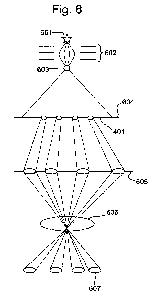
[0075] FIG. 6 shows a tool that is a system for testing the performance of a
sample, such as an
electron-optical assembly, according to embodiments.
[0076] The tool comprises a cathode 601 that is a source of charged particles.
The charged particles
are manipulated by an electro-static lens 602 so as to provide virtual source
603. A sample holder 604
is arranged to hold a sample. The sample may be an electron-optical assembly
401. The tool may
further comprise a scintillator 605, an optical lens 606 and a light detector
607. The light detector 607
may be a photonic sensor. The scintillator is arranged to generate, and emit
from its lower surface, a
light beam in dependence on each beam of charged particle that illuminates
part of the upper surface
of the scintillator. The scintillator may comprise yttrium aluminium garnet
and/or other suitable
materials for scintillation. The optical lens 606 is arranged to focus the
light beams that are emitted
from the scintillator 605. An upper surface of the light detector 607 is
illuminated with light from the
15 optical lens 606. The light detector 607 is arranged to generate signals
corresponding to each beam of
incidence of light. Together the signals comprise detection data in dependence
on the received light.
CA 03168745 2022- 8- 19
WO 2021/165114 16
PCT/EP2021/053190
The detection data may comprise an image of the illuminated areas on the upper
surface of the light
detector 607.
[0077] When the tool is used to test an electron-optical assembly 401, the
upper surface of the
electron-optical assembly 401 is illuminated with a beam of charged particles.
Sub-beams of charged
particles are generated by the aperture array and a plurality of sub-beams of
charged particles are
output from the electron-optical assembly 401. The scintillator 605 is
illuminated by the sub-beams
and generates an optical beam for each sub-beam that it is illuminated. The
light detector 607 then
generates detection data in dependence on the generated optical beams.
[0078] It should be noted that apertures in the aperture array of the electron-
optical assembly may
have any arrangement. In FIG. 6, the pitch, i.e. spacing, between adjacent
apertures is not constant.
However, embodiments also include the pitch between adjacent apertures being
constant. In addition,
the beams may be arranged to cross each other at the center, i.e.mid-point, of
the optical lens 606.
[0079] FIGS. 7A, FIG. 7B and FIG. 7C are examples of images that may be
comprised by, or
generated in dependence on, the detection data.
[0080] FIG. 7A shows the illuminated areas on the surface of the light
detector. Each circular spot
in FIG. 7A corresponds to an optical beam that illuminates the surface of the
light detector. The
position and shape of each of the optical beams is dependent on the shape and
path of a corresponding
sub-beam of charged particles that is generated by, and output from, the
electron-optical assembly.
[00811 FIG. 7A shows an image that has been generated by illuminating an
electron-optical
assembly that comprises aperture, deflector and lens elements. The elements
may be the same as
those described with reference to Figures 4 and 5. However, the number and
arrangement of the
elements differs because the elements are arranged in a 5 by 5 array. All of
the deflector elements are
in a first operation state in which a deflection is not applied to the paths
of the sub-beams. All of the
lens elements are in a first operation state in which a focus is not applied
to the sub-beams.
[0082] FIG. 7B is an image that shows spots that have been generated by
illuminating an electron-
optical assembly when all of the deflector elements are in a second operation
state. In the second
operation state, a deflection is applied to the paths of the sub-beams. FIG.
7B also shows spots in
corresponding positions to the spots in FIG. 7A in order to clearly
demonstrate the differences
between the first and second operation states of the deflector elements. The
magnitude and direction
of the deflection applied by each of the deflector elements can be determined
by comparing the
positions of each of the spots when the deflector elements are in the first
and second operation states.
In the depicted operational test, a common deflection is applied to all of the
deflector elements This
may be a preferred mode of testing. However, any selection of the deflector
elements may be
operated for the operational test.
15 [0083] FIG. 7C is an image that shows spots that have been generated by
illuminating an electron-
optical assembly when all of the lens elements are in a second operation
state. In the second operation
state, a focus is applied to the sub-beams. FIG. 7C also shows spots in
corresponding positions to the
CA 03168745 2022- 8- 19
WO 2021/165114 17
PCT/EP2021/053190
spots in FIG. 7A in order to clearly demonstrate the differences between the
first and second
operation states of the lens elements. The focus applied by each of the lens
elements can be
determined by comparing the size and position of each of the spots when the
lens elements are in the
first and second operation states. In the depicted operational test, a common
focus is applied by all of
the lens elements in the electron-optical assembly. This may be a preferred
mode of testing.
However, any selection of the lens elements may be operated for the
operational test.
[0084] Accordingly, embodiments provide a tool for generating determination
data that can be used
to determine the performance of an electron-optical assembly. Comparisons can
be made between the
measured and expected performances of the manipulation characteristics of
components of the
electron-optical assembly. A determination can be made as to whether or not
the electron-optical
assembly meets all its performance specifications.
[0085] Embodiments also include a number of modifications and variations to
the techniques as
described above.
[0086] In particular, the tool according to embodiments may generate the
detection data in
dependence on other techniques than scintillation. The tool according to
embodiments may therefore
not comprise the above-described scintill ator 605, an optical lens 606 and a
light detector 607. The
tool according to embodiments may alternatively comprise a charged particle
detector. The charged
particle detector may be illuminated by sub-beams of charged particles that
have passed through the
electron-optical assembly. The detection data may be generated in dependence
on the received sub-
beams by the charged particle detector. The charged particle detector may, for
example, be a charge-
coupled device, CCD, pin detector, or CMOS sensor.
[0087] As described above, an electron-optical assembly may comprise a stack
of a plurality of
layers with each layer comprising one or more substrates. One or more of the
layers may comprise an
array of components for manipulating sub-beams. The manufacturing process of
the electron-optical
assembly may therefore comprise a first set of processes for manufacturing
each of the layers to be
included in the stack and a second set of processes for building a stack of
layers.
[0088] The manufacturing process of an electron-optical device comprising the
electron-optical
assembly comprises a further set of processes for attaching and electrically
connecting the stack of
substrates to a PCB.
[0089] An advantage of the tool according to embodiments is that it may be
used to test the
components of the electron-optical assembly during the different stages of
construction of the
electron-optical assembly in addition to an electron-optical device.
[0090] In particular, electrical connectors may be temporarily applied to any
one of the layers that
comprises an array of components so that the operation state of the components
may be controlled.
15 The tool according to embodiments may therefore be used to determine if
the performance of an
individual layer is within its performance specifications before separate
layers are built together into a
CA 03168745 2022- 8- 19
WO 2021/165114 18
PCT/EP2021/053190
stack. The term electron-optical assembly, as used herein. may therefore refer
to a single layer or a
stack comprising a plurality of layers.
[0091] The tool according to embodiments may also be used to determine if the
performance of the
final stack of substrates is within its performance specification before the
stack is attached to its
supporting structure, such as a PCB. Advantageously, the tool allows any
defective layers and/or
stacks to be quickly determined and manufacturing costs to thereby be reduced.
A stack of substrates
does not meet its performance specifications may he removed from the electron-
optical device
production process.
[0092] Another advantage of the tool according to embodiments is that the
performance of an
electron-optical assembly can be determined using a charged particle source
that is operated at a lower
power than the charged particle source in a charged particle apparatus for SEM
or lithography. The
charged particle source in the tool according to embodiments needs to only be
powerful enough for
the sub-beams that have passed through the electron-optical assembly to be
detected. Sources with
substantially higher power, for example amongst other specific characteristic
requirements, are
required in charged particle apparatuses for applications such as SEM and
lithography. However,
embodiments also include testing the electron-optical assembly with the same
power of charged
particles that the electron-optical assembly will be used with when it is
installed in a charged particle
apparatus. Such a test may be more accurate because any performance
differences that are dependent
on the power of the charged particles would be avoided.
[0093] The tool according to embodiments may typically be operated with
electron beam that has the
properties: 5keV, 125p A beam, spread over a beam with diameter of about lcm.
However, the
operational range of the tool may be over a wide range. For example, the
electron beam properties
may be: lkeV-30keV, 1pA-1 IRA beam, spread over a beam with diameter of about
of 0.1mm to 20-
30cm.
[0094] In a charged particle apparatus for SEM or lithography, the properties
of the electron beam
may be: 30keV, 5nA or larger. The spot size of each beam may vary from 0.1 am
to 100nm.
[0095] Operating with low power charged particle sources may be safer, easier
and cheaper. For
example, it may reduce the amount x-rays that are generated and the measures
necessary to protect
operators from x-rays. In addition, a source with lower power requirements
than those required for
SEM or lithographic applications is more commercially available.
[0096] The tool according to embodiments has been described with reference to
an electron-optical
assembly for manipulating a multi-beam of charged particles. Embodiments also
include the tool
being used to determine the performance of an electron-optical assembly for
manipulating a single
beam of charged particles. Embodiments also include the tool being used to
determine the
15 performance of other types of sample than an electron-optical assembly.
CA 03168745 2022- 8- 19
WO 2021/165114 19
PCT/EP2021/053190
[0097] The tool according embodiments may comprise one or more computing
devices for
determining the performance of the electron-optical assembly, or other sample,
that is tested by the
tool in dependence on the detection data generated by the tool.
[0098] The tool according embodiments may comprise one Or more computing
devices for
controlling the operation of the tool and/or electron-optical assembly, or
other sample, that is tested by
the tool.
[0099] Embodiments also include techniques for determining and analysing the
properties of features
in images. The techniques according to embodiments may improve the accuracy
with which the
contour, i.e. edge points, of each feature can be determined. The techniques
according to
embodiments may also provide efficient techniques for analysing features. The
techniques according
to embodiments are particularly appropriate for analysing images such as those
shown in FIGS. 7A to
7C.
[00100]FIGS. 7A to 7C, all show a plurality of substantially circular
features, with each feature
corresponding to the aperture through a component of a MEMS array. The
performance of the
components in the MEMS array can be determined in dependence on an analysis of
the substantially
circular features with the MEMS array in any operating state. For example the
circular properties of
each of the features and/or relative positions of each of the features may be
determined. As described
earlier, the performance of the components in the MEMS array may also be
determined in dependence
on a comparison of the features in images generated with the components of the
MEMS array in
different operating states.
[00101]FIGS. 8, 9A and 9B show a technique for determining the position of
each of a plurality of
points on the edge of an imaged substantially circular feature according to
embodiments. As shown in
FIG. 8, embodiments include determining an approximate location of the center
point of the feature.
Intensity measurements are then obtained at a plurality of locations on each
of a plurality of straight
lines that each extend from the determined center point of the feature to a
point outside of the feature.
On each straight line, intensity measurements are therefore obtained on either
side of the edge of the
feature. The angular spacing between adjacent ones of the plurality of
straight lines may be equal.
[00102]FIG. 9A shows how the actual intensity profile may vary along one of
the straight lines that
extends from the determined center point of the feature. In FIG. 9A, the x-
axis 901 corresponds to a
distance, on the straight line, from the determined center point of the image.
The y-axis corresponds
to an intensity value, such as a grey value, at each position on the axis. The
continuous intensity
profile 902 varies along the x-axis 901. At the center point of the feature,
the intensity profile may be
at a local minimum value, indicated by the intensity values at the leftmost
part of FIG. 9A. On the
other side of the edge of the feature, i.e. at positions outside of the
feature, the intensity profile may be
15 at a local maximum value, indicated by the intensity values at the
rightmost part of FIG. 9A. A point
on the edge of the feature may be determined as the point on the x-axis 901 at
which the intensity is
the mid-intensity between the local maximum and local minimum intensities.
This approach
CA 03168745 2022- 8- 19
WO 2021/165114 20
PCT/EP2021/053190
determines the edge position to be at the x-axis location 903. However, the
intensity measurements
along the line are measurements at discrete points along the line and not the
continuous measurement
shown in FIG. 9A. FIG. 9B shows the location of discrete regularly spaced
intensity measurement
pixels on the same straight line as that shown in FIG. 9A. For each pixel, the
intensity value of the
pixel may be determined in dependence on a bilinear interpolation of the
intensity values of the four
nearest pixels to said pixel. The intensity values may be grey values.
[00103] According to known techniques for determining the location of the edge
of the feature, the
location on the x-axis 901 that corresponds to the mid-intensity between the
local maximum and local
minimum intensities is determined by linear interpolation between the
locations of the discrete
intensity measurement points on either side of the mid-intensity value. As
shown in FIG. 9B, the
linearly interpolated line 905 determines the x-axis 901 position of the edge
to be at 906 instead of
903. The difference along the x-axis 901 between 906 and 903 is therefore an
error in the
determination of the location of a point in the edge of the feature.
100104] Embodiments provide an alternative technique for determining the x-
axis 901 position that
corresponds to the mid-intensity between the local maximum and local minimum
intensities. The
theoretically ideal intensity profile shown in FIG. 9A mathematically
corresponds to the convolution
of an Airy disc with a step function. Embodiments include approximating the
Airy disc with a
Gaussian function. The convolution of the Gaussian function with a step
function gives an Error
function. Embodiments include fitting the Error function to the discrete
intensity measurements to
thereby generate an estimated intensity profile 904 as shown in FIG. 9B. The x-
axis position
corresponding to the mid-intensity between the local maximum and local minimum
intensities is then
determined in dependence on the estimated intensity profile 904.
100105]Embodiments may therefore provide a substantially more accurate
technique for determining
the location of a point on the edge of the feature than known techniques.
Embodiments include
determining the location of each of a plurality of points on the edge of the
feature in dependence on a
respective plurality of straight lines, as shown in FIG. 8, and an estimated
intensity profile 904, as
described with reference to FIG. 9B. The plurality of points on the edge of
the feature may be used to
determine a contour of the feature.
[00106] Embodiments also include techniques for analysing the contour angular
errors, i.e. circular
properties, of each feature in an image.
100107] For each feature in an image, a plurality of points on the edge of the
feature may be
determined according the techniques of the above-described embodiment, or
other image analysis
techniques. FIG. 10A shows such points on the edge of a feature. Each of the
points on the edge of
the feature is converted to a polar coordinate representation so that it is
represented by {R, 0} values,
15 as shown in FIG. 1011, The {R, 0} values are a polar coordinate dataset
for the points on the edge of
the feature. A transform operation is then applied to the polar coordinate
dataset. The transform
CA 03168745 2022- 8- 19
WO 2021/165114 21
PCT/EP2021/053190
operation may be a Fourier Transform, such as the Fast Fourier Transform (FFT)
or Discrete Fast
Fourier Transform (DFFT).
[00108]FIG. 10C shows image analysis results that may be generated by applying
an FFT to the
polar coordinate dataset in FIG. 10B. In FIG. 10C, the x-axis provides orders
of wave numbers and
the y-axis provides angular error values. The 0111 order wave number indicates
the radius of the
feature. The 1" order wave number indicates the difference between the
determined center point of
the feature for generating the polar coordinates and an actual center of the
feature. The 2 order wave
number is a measure of the elliptical properties of the feature. The 3rd and
higher order wave numbers
are indicative of higher order aberrations in the contour of the feature.
[00109]By using the above-described techniques, embodiments allow the contour
angular errors, i.e.
circular properties, of a feature to be easily and efficiently determined.
[00110]The above described techniques according to embodiments are not
restricted to use with
circular features. Embodiments include the techniques being used to determine
the location of points
on the edge of a feature with any shape and/or the analysis of features with
substantially non-circular
contours. When the techniques are used in the analysis of features with
substantially non-circular
contours, the 2' order wave number, and higher wave numbers, may comprise a
component that is
related to the shape of the contour and not just aberrations.
[00111]In addition, the above described techniques according to embodiments
are not restricted to the
specific application of an analysing an image obtained in the testing of an
electron-optical assembly.
The techniques may be used more generally in the analysis of images obtained
in any application,
such as a metrology or inspection application.
[00112]The tool according to embodiments allows the testing of the performance
of an electron-
optical assembly. The performance may be determined in a number of different
ways. For example,
the tool may simply indicate either that the electron-optical assembly passes
a test or that it fails a test.
For example, the electron-optical assembly may be controlled so that correct
operation will deflect all
of the beams being tested to the right. If the beams being tested are all
deflected to the right by more
than a minimum amount, then the result of the test is a pass regardless of the
actual magnitude and
specific direction of the deflection amount. The tool may separately provide
the circular properties of
each beam using the above-described techniques.
[00113]The tool may additionally, or alternatively, provide a qualitative
measurement of a
performance aspect. For example, in addition to providing the circular
properties of each beam, it
may determine and output the specific magnitude and direction of the
deflection of each beam. These
properties could be provided alongside data on the applied deflection
voltages, e-heam energies and
other operating conditions.
15 [00114]The tool may additionally, or alternatively, test the electrical
connections to each element in
the electron-optical assembly. The numerous electrical connection paths that
connect a controller to
each of the electrodes of the elements may require some long and difficult
routing and linking. The
CA 03168745 2022- 8- 19
WO 2021/165114 22
PCT/EP2021/053190
test output may therefore be a determination of whether or not the electrical
connection paths for the
electron-optical assembly are all correct.
[00115] The tool may additionally, or alternatively, determine that the
elements in the electron-optical
assembly are appropriately located for alignment with the sub-beams of a multi-
beam. However, the
deflection, or focus, performance of the elements may not be tested.
[00116] Embodiments include a number of modifications and variations to the
techniques described
above.
[00117] An electron-optical device that is tested and made according to
embodiments may be used in
a multi-beam charged particle apparatus. The multi-beam charged particle
apparatus may be a
component of an inspection (or metro-inspection) tool or part of an e-beam
lithography tool. The
multi-beam charged particle apparatus may be used in a number of different
applications that include
electron microscopy in general, not just SEM, and lithography. The multi-beam
charged particle
apparatus may comprise more than one source of charged particles.
[00118]In the embodiment described with reference to FIGS. 9A and 9B, at the
center point of the
feature the intensity profile is at a local minimum value and on the other
side of the edge of the
feature the intensity profile is at a local maximum value. Embodiments also
include alternative
applications, and ways of generating images, in which at the center point of
the feature the intensity
profile is at a local maximum value and on the other side of the edge of the
feature the intensity
profile is at a local minimum value.
[00119] Embodiments include the following statements.
[00120] According to a first aspect of the invention, there is provided an
electron-optical assembly
testing system for testing an electron-optical assembly, the system
comprising: a source of charged
particles configured to emit a beam of charged particles; an electron-optical
assembly holder
configured to hold an electron-optical assembly to be tested such that, when
the system is in use with
an electron-optical assembly held by the electron-optical assembly holder, the
electron-optical
assembly is illuminated by the beam; and a sub-beam detector for detecting sub-
beams of charged
particles that have been transmitted through the electron-optical assembly.
[00121] Preferably, the sub-beam detector comprises a scintillator configured
to emit a plurality of
sub-beams of light in dependence on respective plurality of sub-beams of
charged particles incident
on the scintillator.
[00122] Preferably, the sub-beam detector comprises a photonic sensor
configured to detect each sub-
beam of light corresponding to each incidental sub-beam of charged particles.
[00123] Preferably, the sub-beam detector comprises a detection data generator
configured to generate
detection data in dependence on sub-beams of light incident on the photonic
sensor.
15 [00124] Preferably, the scintillator comprises yttrium aluminium garnet.
CA 03168745 2022- 8- 19
WO 2021/165114 23
PCT/EP2021/053190
[00125] Preferably, the sub-beam detector is configured to: sense the sub-
beams of charged particles
incident on the sub-beam detector; and generate detection data in dependence
on the incident sub-
beams of charged particles.
[00126] Preferably, the sub-beam detector is a charge-coupled device, CCD, p/n
detector and/or
CMOS sensor.
[00127] Preferably, the detection data is suitable for generating one or more
images that are indicative
of the focus and or deflection states of the sub-beams of charged particles.
[00128] Preferably, the system further comprises one or more computing
devices, wherein each
computing device is configured to: determine the performance of an electron-
optical assembly; and/or
control the test of an electron-optical assembly by the electron-optical
assembly testing system.
[00129] Preferably, the electron-optical assembly is configured to
simultaneously manipulate each of
a plurality of beams of charged particles.
[00130] Preferably, a computing device is configured to control the test of
the deflection and/or focus
of an electron-optical assembly.
[00131] Preferably, the electron-optical assembly comprises a stack of layers;
each layer in the stack
comprises one or more substrates; and one or more layers in the stack
comprises a plurality of MEMS
components.
[00132] Preferably, the electron-optical assembly is comprised by an electron-
optical device for use in
a charged particle apparatus for SEM or lithography.
[00133] According to a second aspect of the invention, there is provided a
method of testing an
electron-optical assembly, the method comprising: illuminating the electron-
optical assembly with at
least one beam of charged particles such that charged particles in the at
least one beam are transmitted
through the electron-optical assembly in a plurality of sub-beams; detecting
sub-beams of charged
particles that have been transmitted through the electron-optical assembly;
and determining the
performance of the electron-optical assembly in dependence on the detected sub-
beams; wherein the
test of the determination of the performance of the electron-optical assembly
is made prior to use of
an electron-optical device, that comprises the electron-optical assembly, in a
charged particle
apparatus for SEM or lithography.
[00134] Preferably, said step of detecting sub-beams of charged particles that
have been transmitted
through the electron-optical assembly comprises: generating, by scintillation,
a plurality of sub-beams
of light that respectively correspond to the sub-beams of charged particles;
detecting each of the
plurality of sub-beams of light; and generating a detection data signal in
dependence on the sub-beams
of light.
[00135] Preferably, said step of detecting sub-beams of charged particles that
have been transmitted
15 through the electron-optical assembly comprises: detecting the sub-beams
of charged particles
transmitted from the electron-optical assembly; and generating a detection
data signal in dependence
on the detected sub-beams of charged particles.
CA 03168745 2022- 8- 19
WO 2021/165114 24
PCT/EP2021/053190
[00136] Preferably, the sub-beams are detected by a charge-coupled device,
CCD, p/n detector and/or
CMOS sensor.
[00137] Preferably, said step of determining the performance of the electron-
optical assembly in
dependence on the detected sub-beams comprises determining the performance of
the electron-optical
assembly in dependence on the detection data signal.
[00138] Preferably, the method further comprises using detection data in the
detection data signal to
generate one or more images.
[00139] Preferably, the electron-optical assembly is configured to deflect the
paths of the sub-beams
and/or focus the sub-beams so that the detection data corresponds to the sub-
beam deflection and/or
performance of the electron-optical assembly.
[00140] Preferably, determining the performance of the electron-optical
assembly comprises
comparing a determined deflection and/or focus against an expected deflection
and/or focus.
[00141] Preferably, the power of the at least one beam of charged particles
that the electron-optical
assembly is illuminated with is less that the power that the electron-optical
device is illuminated with
when it is used in the charged particle apparatus for SEM or lithography.
[00142] Preferably, the method further comprises determining to comprise the
electron-optical
assembly in an electron-optical device in dependence on the determined
performance of the electron-
optical assembly.
[00143] Preferably, the method further comprises determining to use the
electron-optical device a
charged particle apparatus for SEM or lithography.
[00144] Preferably, the method further comprises: generating a first image
when the electron-optical
assembly is in a first sub-beam deflection state; generating a second image
when the electron-optical
assembly is in a second sub-beam deflection state that is different from the
first sub-beam deflection
state; determining the deflection performance of the electron-optical assembly
in dependence on a
comparison of the first image and the second image.
[00145] Preferably, the method further comprises: generating a first image
when the electron-optical
assembly is in a first sub-beam focus state; generating a second image when
the electron-optical
assembly is in a second sub-beam focus state that is different from the first
sub-beam focus state; and
determining the focus performance of the electron-optical assembly in
dependence on a comparison of
the first image and the second image.
[00146] Preferably, the electron-optical assembly comprises a stack of layers;
each layer in the stack
comprises one or more substrates; and one or more layers in the stack
comprises a plurality of MEMS
components arranged in an array.
[00147] Preferably, the electron-optical assembly is comprised by an electron-
optical device for use in
15 a charged particle apparatus for SEM or lithography.
CA 03168745 2022- 8- 19
WO 2021/165114 25
PCT/EP2021/053190
[00148] Preferably, the method of testing an electron-optical assembly is
performed during the
manufacture of an electron-optical device for use in a charged particle
apparatus for SEM or
lithography.
[00149] Preferably, the method further comprises: generating an image
comprising a plurality of
features in dependence on the detection data signal; and estimating, for each
feature, the positions of a
plurality of points on the edge of the feature; wherein estimating the
position of each point on the
edge of each feature comprises: obtaining a plurality of discrete intensity
measurements at positions
on a straight line that crosses the edge of the feature; fitting an Error
function to the plurality of
intensity measurements; using the Error function to determine a mid-point
between local maximum
and minimum values of the intensity measurements; and estimating the position
of the point on the
edge of the feature in dependence on the determined mid-point.
[00150] Preferably, estimating the position of each point on the edge of the
feature further comprises:
estimating the position of the center of the feature; and determining, for
each of the plurality of points
on the edge of the feature, a plurality of discrete intensity measurements at
positions that lie on a
straight line that intersects the estimated position of the center of the
feature and the edge of the
feature.
[00151] Preferably, the method further comprises determining a contour of each
feature in dependence
on the determined positions of the points on the edge of each feature.
[00152]Preferably, the method further comprises analysing the properties of
the contour of each
feature; wherein analysing the properties of the contour of each feature
comprises: obtaining, for each
feature, estimated positions of a plurality of points on the edge of the
feature; converting the obtained
plurality of discrete points into a dataset of polar coordinates; generating a
plurality of values of wave
numbers by performing a transform on the dataset of polar coordinates; and
using one or more values
of the wave numbers to analyse the properties of the imaged contour of the
feature.
[00153]Preferably, the circular properties of the imaged contour of the
feature are determined.
[00154] Preferably, the transform is a Fourier Transform.
[00155] Preferably, each feature in the image corresponds to an opening in a
component for
manipulating one or more electron beams.
[00156]According to a third aspect of the invention, there is provided a
method of manufacturing an
electron-optical device that comprises an electron-optical assembly, the
method comprising: testing an
electron-optical assembly according to the method of the second aspect; and
determining to construct
an electron-optical device that comprises the electron-optical assembly in
dependence on the test.
[00157] According to a fourth aspect of the invention, there is provided an
electron-optical assembly
testing system for testing an electron-optical assembly, the system
comprising: a source of charged
15 particles configured to emit a beam of charged particles; an electron-
optical assembly holder
configured to hold an electron-optical assembly for testing the electron-
optical assembly by
transmission of charged particle beams from the source through the electron-
optical assembly; and a
CA 03168745 2022- 8- 19
2019P00328W0CA 26
sub-beam detector configured to detect sub-beams of charged particles
transmitted from the source
through the electron-optical assembly held by the holder.
[00158]Preferably, the electron-optical assembly testing system is configured
to perform the method
according to the second aspect.
[00159] While the present invention has been described in connection with
various embodiments,
other embodiments of the invention will be apparent to those skilled in the
art from consideration of
the specification and practice of the invention disclosed herein. It is
intended that the specification and
examples be considered as exemplary only. with a true scope and spirit of the
invention being
indicated by the following claims.
[00160] The descriptions above are intended to be illustrative, not limiting.
Thus, it will be apparent
to one skilled in the art that modifications may be made as described without
departing from the scope
of the claims and clauses as set out below.
[00161] There is provided the following clauses:
[00162] Clause 1: An electron-optical assembly testing system for testing an
electron-optical
assembly, the system comprising: a source of charged particles configured to
emit a beam of charged
particles; an electron-optical assembly holder configured to hold an electron-
optical assembly to be
tested such that, when the system is in use with an electron-optical assembly
held by the electron-
optical assembly holder, the electron-optical assembly is illuminated by the
beam; and a sub-beam
detector for detecting sub-beams of charged particles that have been
transmitted through the electron-
optical assembly.
[00163] Clause 2: The system according to clause 1, wherein the sub-beam
detector comprises: a
scintillator configured to emit a plurality of sub-beams of light in
dependence on respective plurality
of sub-beams of charged particles incident on the scintillator; and a photonic
sensor configured to
detect each sub-beam of light corresponding to each incidental sub-beam of
charged particles;
wherein the system, further comprises a detection data generator configured to
generate detection data
in dependence on sub-beams of light incident on the photonic sensor.
[00164] Clause 3: The system according to clause 2, wherein the scintillator
comprises yttrium
aluminum garnet.
[00165] Clause 4: The system according to clause 1, wherein the sub-beam
detector is configured to:
sense the sub-beams of charged particles incident on the sub-beam detector;
and generate detection
data in dependence on the incident sub-beams of charged particles.
[00166] Clause 5: The system according to clause 4, wherein the sub-beam
detector is a charge-
coupled device, CCD, p/n detector and/or CMOS sensor.
[00167] Clause 6: The system according to any of clauses 2 to 5, wherein the
detection data is suitable
for generating one or more images that are indicative of the focus and or
deflection states of the sub-
beams of charged particles.
CA 03168745 2022- 8- 19
2019P00328W0CA 27
[00168] Clause 7: The system according to any preceding clause, further
comprising one or more
computing devices, wherein each computing device is configured to: determine
the performance of
an electron-optical assembly; and/or control the test of an electron-optical
assembly by the electron-
optical assembly testing system.
[00169] Clause 8: The system according to any preceding clause, wherein the
electron-optical
assembly is configured to simultaneously, or individually, manipulate each of
a plurality of beams of
charged particles.
[00170] Clause 9: The system according to clause 8, wherein a computing device
is configured to
control the test of the deflection and/or focus of an electron-optical
assembly.
[00171] Clause 10: The system according to any preceding clause, wherein the
electron-optical
assembly comprises a stack of layers; each layer in the stack comprises one or
more substrates; and
one or more layers in the stack comprises a plurality of MEMS components.
[00172] Clause 11: The system according to any preceding clause, wherein the
electron-optical
assembly is comprised by an electron-optical device for use in a charged
particle apparatus for SEM
or lithography.
[00173] Clause 12: A method of testing an electron-optical assembly, the
method comprising:
illuminating the electron-optical assembly with at least one beam of charged
particles such that
charged particles in the at least one beam are transmitted through the
electron-optical assembly in a
plurality of sub-beams; detecting sub-beams of charged particles that have
been transmitted through
the electron-optical assembly; and determining the performance of the electron-
optical assembly in
dependence on the detected sub-beams; wherein the test of the determination of
the performance of
the electron-optical assembly is made prior to use of an electron-optical
device, that comprises the
electron-optical assembly, in a charged particle apparatus for SEM or
lithography.
[00174] Clause 13: The method according to clause 12, wherein said step of
detecting sub-beams of
charged particles that have been transmitted through the electron-optical
assembly comprises:
generating, by scintillation, a plurality of sub-beams of light that
respectively correspond to the sub-
beams of charged particles; detecting each of the plurality of sub-beams of
light; and generating a
detection data signal in dependence on the sub-beams of light.
[00175] Clause 14: The method according to clause 12, wherein said step of
detecting sub-beams of
charged particles that have been transmitted through the electron-optical
assembly comprises:
detecting the sub-beams of charged particles transmitted from the electron-
optical assembly; and
generating a detection data signal in dependence on the detected sub-beams of
charged particles.
[00176] Clause 15: The method according to clause 14, wherein the sub-beams
are detected by a
charge-coupled device, CCD, p/n detector and/or CMOS sensor.
[00177] Clause 16: The method according to any of clauses 13 to 15, wherein
said step of determining
the performance of the electron-optical assembly in dependence on the detected
sub-beams comprises
CA 03168745 2022- 8- 19
2019P00328W0CA 28
determining the performance of the electron-optical assembly in dependence on
the detection data
signal.
[00178] Clause 17: The method according to any of clauses 13 to 16, further
comprising using
detection data in the detection data signal to generate one or more images.
[00179] Clause 18: The method according to any of clauses 12 to 17, wherein
the electron-optical
assembly is configured to deflect the paths of the sub-beams and/or focus the
sub-beams.
[001801 Clause 19: The method according to clause 18, wherein determining the
performance of the
electron-optical assembly comprises comparing a determined deflection and/or
focus against an
expected deflection and/or focus.
[00181] Clause 20: The method according to any of clauses 12 to 19, wherein
the power of the at least
one beam of charged particles that the electron-optical assembly is
illuminated with is less that the
power that the electron-optical device is illuminated with when it is used in
the charged particle
apparatus for SEM or lithography.
[00182] Clause 21: The method according to any of clauses 12 to 20, the method
further comprising
determining to comprise the electron-optical assembly in an electron-optical
device in dependence on
the determined performance of the electron-optical assembly.
[00183] Clause 22: The method according to clause 21, the method further
comprising determining to
use the electron-optical device a charged particle apparatus for SEM or
lithography.
[00184] Clause 23: The method according to any of clauses 12 to 22, the method
further comprising:
generating a first image when the electron-optical assembly is in a first sub-
beam deflection state;
generating a second image when the electron-optical assembly is in a second
sub-beam deflection
state that is different from the first sub-beam deflection state; and
determining the deflection
performance of the electron-optical assembly in dependence on a comparison of
the first image and
the second image.
[00185] Clause 24: The method according to any of clauses 12 to 23, the method
further comprising:
generating a first image when the electron-optical assembly is in a first sub-
beam focus state;
generating a second image when the electron-optical assembly is in a second
sub-beam focus state
that is different from the first sub-beam focus state; and determining the
focus performance of the
electron-optical assembly in dependence on a comparison of the first image and
the second image.
[00186] Clause 25: The method according to any of clauses 12 to 24, wherein
the electron-optical
assembly comprises a stack of layers; each layer in the stack comprises one or
more substrates; and
one or more layers in the stack comprises a plurality of MEMS components
arranged in an array.
[00187] Clause 26: The method according to clause 25, wherein the electron-
optical assembly is
comprised by an electron-optical device for use in a charged particle
apparatus for SEM or
lithography.
CA 03168745 2022- 8- 19
2019P00328W0CA 29
[00188] Clause 27: The method according to any of clauses 12 to 26, wherein
the method of testing an
electron-optical assembly is performed during the manufacture of an electron-
optical device for use in
a charged particle apparatus for SEM or lithography.
[00189] Clause 28: The method according to any of clauses 12 to 27, the method
further comprising:
generating an image comprising a plurality of features in dependence on the
detection data signal; and
estimating, for each feature, the positions of a plurality of points on the
edge of the feature; wherein
estimating the position of each point on the edge of each feature comprises:
obtaining a plurality of
discrete intensity measurements at positions on a straight line that crosses
the edge of the feature;
fitting an Error function to the plurality of intensity measurements; using
the fitted Error function to
determine a mid-point between local maximum and minimum values of the
intensity measurements;
and estimating the position of the point on the edge of the feature in
dependence on the determined
mid-point.
[00190] Clause 29: The method according to clause 28, wherein estimating the
position of each point
on the edge of the feature further comprises: estimating the position of the
center of the feature; and
determining, for each of the plurality of points on the edge of the feature, a
plurality of discrete
intensity measurements at positions that lie on a straight line that
intersects the estimated position of
the center of the feature and the edge of the feature.
[00191] Clause 30: The method according to clause 28 or 29, further comprising
determining a
contour of each feature in dependence on the determined positions of the
points on the edge of each
feature.
[00192] Clause 31: The method according to any of clauses 28 to 30, further
comprising analyzing the
properties of the contour of each feature; wherein analyzing the properties of
the contour of each
feature comprises: obtaining, for each feature, estimated positions of a
plurality of points on the edge
of the feature; converting the obtained plurality of discrete points into a
dataset of polar coordinates;
generating a plurality of values of wave numbers by performing a transform on
the dataset of polar
coordinates; and using one or more values of the wave numbers to analyze the
properties of the
imaged contour of the feature.
[00193] Clause 32: The method according to clause 31, wherein the circular
properties of the imaged
contour of the feature are determined.
[00194] Clause 33: The method according to clause 31 or 32, wherein the
transform is a Fourier
Transform.
[00195] Clause 34: The method according to any of clauses 28 to 33, wherein
each feature in the
image corresponds to an opening in a component for manipulating one or more
electron beams.
[00196] Clause 35: A method of manufacturing an electron-optical device that
comprises an electron-
optical assembly, the method comprising: testing an electron-optical assembly
according to the
method of any of clauses 12 to 34; and determining to construct an electron-
optical device that
comprises the electron-optical assembly in dependence on the test.
CA 03168745 2022- 8- 19
2019P00328W0CA 30
[00197] Clause 36: An electron-optical assembly testing system for testing an
electron-optical
assembly, the system comprising: a source of charged particles configured to
emit a beam of charged
particles; an electron-optical assembly holder configured to hold an electron-
optical assembly for
testing the electron-optical assembly by transmission of charged particle
beams from the source
through the electron-optical assembly; and a sub-beam detector configured to
detect sub-beams of
charged particles transmitted from the source through the electron-optical
assembly held by the
holder.
[00198] Clause 37: The electron-optical assembly testing system according to
clause 36, wherein the
electron-optical assembly testing system is configured to perform the method
according to any of
clauses 12 to 34.
[00199] Clause 38: An electron-optical assembly testing system for testing an
electron-optical
assembly, the system comprising: a source of charged particles configured to
emit a beam of charged
particles; an electron-optical assembly holder configured to hold an electron-
optical assembly for
testing the electron optical assembly by transmission of charged particle
beams from the source
through the electron optical assembly; and a sub-beam detector configured to
detect sub-beams of
charged particles transmitted from the source through the electron-optical
assembly held by the
holder.
[00200] Clause 39: The system according to clause 38, wherein the sub-beam
detector is a scintillator
configured emit a plurality of sub-beams of light in dependence on respective
plurality of sub-beams
of charged particles incident on the scintillator; and the system further
comprises a detection data
generator configured to generate detection data in dependence on sub-beams of
light incident on the
detection data generator.
CA 03168745 2022- 8- 19