Note : Les descriptions sont présentées dans la langue officielle dans laquelle elles ont été soumises.
WO 2021/195063
PCT/US2021/023649
IMPRINTING APPARATUS
CROSS-REFERENCE TO RELATED APPLICATIONS
[0001] This application claims the benefit of U.S.
Provisional Application
Serial Number 63/000,964, filed March 27, 2020, the contents of which is
incorporated by reference herein in its entirety.
BACKGROUND
[0002] Nano-imprinting technology may enable the economic
and effective
production of nanostructures. Nano-imprint lithography employs direct
mechanical
deformation of a resist material by a stamp having nanostructures. The resist
material is cured while the stamp is in place to lock the shape of the
nanostructures
in the resist material.
[0003] Nano-imprint lithography has been used to manufacture
patterned
substrates, which may be used in a variety of applications. Some patterned
substrates include fluidic channels and discrete wells or depressions. These
patterned substrates may be built into flow cells. In some flow cells, active
surface
chemistry is introduced into the discrete depressions, while interstitial
regions
surrounding the discrete depressions remain inert. These flow cells may be
particularly useful for detection and evaluation of a wide range of molecules
(e.g.,
deoxyribonucleic acid (DNA)), families of molecules, genetic expression
levels, or
single nucleotide polymorphisms.
INTRODUCTION
[0004] In a first aspect, an imprinting apparatus comprises
a silicon master
including a plurality of features positioned at an average pitch of less than
about
425 nm, each of the plurality of features comprising a depression having an
opening with its largest opening dimension being less than about 300 nm; and
an
anti-stick layer coating a surface of the silicon master, the anti-stick layer
including
a crosslinked silane polymer network.
[0005] In an example of the first aspect, less than about
0.15% of a total
number of the plurality of features has a membrane defect.
CA 03173685 2022- 9- 27
WO 2021/195063
PCT/US2021/023649
[0006] In an example of the first aspect, the anti-stick
layer is generated with
a formulation including: a first silane monomer:
o
/
\ 1
0
.0
= õ
=
/ Q
N5z
0 * +=\
\ 0
=
=
=
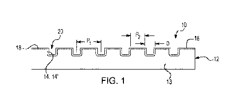
and less than about 1.4 wt%, based on a total amount of silanes present in the
formulation, of a second silane monomer including a hydrolyzable chloride
group.
[0007] In an example of the first aspect, the anti-stick
layer coats a wall of
each of the depressions without capping the opening or without fully filling
the
depression.
[0008] In an example of the first aspect, the largest
opening dimension of
each of the plurality of features ranges from about 170 nm to about 290 nm.
[0009] In an example of the first aspect, the largest
opening dimension of
each of the plurality of features ranges from about 200 nm to about 250 nm.
[0010] In an example of the first aspect, the average pitch
ranges from about
340 nm to about 410 nm.
[0011] In an example of the first aspect, the average pitch
ranges from about
350 nm to about 400 nm.
[0012] It is to be understood that any features of the
imprinting apparatus
disclosed herein may be combined together in any desirable manner and/or
configuration to achieve the benefits as described in this disclosure,
including, for
example, generating small, high-resolution features in a working stamp that is
made using the imprinting apparatus and/or facilitating clean release of the
working
stamp that is made from the imprinting apparatus.
2
CA 03173685 2022- 9- 27
WO 2021/195063
PCT/US2021/023649
[0013] In a second aspect, a method comprises applying a
formulation on a
silicon master including a plurality of features positioned at an average
pitch of less
than about 425 nm, each of the plurality of features having a largest opening
dimension being less than about 300 nm, the formulation including: a first
silane
monomer:
1 a
/
/
......
1
=
=
f
N .
=
and less than about 1.4 wt%, based on a total amount of silanes present in the
formulation, of a second silane monomer including a hydrolyzable chloride
group;
and curing the applied formulation, thereby forming an anti-stick layer.
[0014] In an example of the second aspect, the second silane
monomer is:
./
/
/
/
\
3
CA 03173685 2022- 9- 27
WO 2021/195063
PCT/US2021/023649
In some of these examples, the formulation includes from about 0.28 wt% to
about
1.1 wt% of the second silane monomer.
[0015] In an example of the second aspect, the formulation
further includes:
I) a dimer including two bonded units of the first silane monomer; ii) a
trimer
including three bonded units of the first silane monomer; iii) a higher
molecular
species including more than three bonded units of the first silane monomer;
iv) the
first silane monomer having at least one hydrolyzed ethoxy group; or v) any
combination of i, ii, iii, and iv.
[0016] In an example of the second aspect, curing involves:
an incubation
process; a rinsing process after the incubation process; and a heating process
after
the rinsing process. In some of these examples, the incubation process and the
heating processes are independently performed at a temperature ranging from
about 20 C to about 250 C, for a time ranging from about 1 minute to about 30
minutes.
[0017] An example of the second aspect, further comprises
generating the
formulation by: diluting a neat silane material including the first and second
silane
monomers in a first solvent to form a precursor solution; exposing the
precursor
solution to an aqueous, basic solution to generate an aqueous phase and an
organic phase, wherein the organic phase includes the first solvent; removing
the
aqueous phase; removing the first solvent from the organic phase to obtain a
purified silane material; and diluting the purified silane material in a
second solvent.
In some of these examples, the second solvent is an aprotic solvent that i)
solvates
the purified silane material and ii) has a boiling point ranging from about 50
C to
about 250 C. In some of these examples, the purified silane material is
present in
the formulation in an amount ranging from about 1 wt% to about 20 wt%.
[0018] In an example of the second aspect, applying the
formulation involves
spin coating.
[0019] In an example of the second aspect, one of: the
formulation is solvent
free; or the formulation includes from about 1 wt% to about 20 wt% of the
first
silane monomer.
[0020] It is to be understood that any features of this
method may be
combined together in any desirable manner. Moreover, it is to be understood
that
any combination of features of the method and/or of the imprinting apparatus
may
4
CA 03173685 2022- 9- 27
WO 2021/195063
PCT/US2021/023649
be used together, and/or combined with any of the examples disclosed herein to
achieve the benefits as described in this disclosure, including, for example,
to
generate small, high-resolution features in an imprinting stamp and/or a
working
stamp that is made using the imprinting apparatus, and/or to facilitate clean
release
of the working stamp that is made from the imprinting apparatus.
[0021] In a third aspect, another method comprises forming
an imprinting
apparatus by: depositing a formulation on a silicon master including a
plurality of
features positioned at an average pitch of less than about 425 nm, each of the
plurality of features having a largest opening dimension of less than about
300 nm,
and the formulation including: a first silane monomer:
=
\
\
=
, 0--
,
o
=
and less than 1.4 wt%, based on a total amount of silanes present in the
formulation, of a second silane monomer including a hydrolyzable chloride
group;
and curing the formulation, thereby forming an anti-stick layer on the silicon
master;
depositing a silicon-based working stamp material on the anti-stick layer of
the
imprinting apparatus; curing the silicon-based working stamp material to form
a
working stamp including a negative replica of the plurality of features; and
releasing
the working stamp from the imprinting apparatus.
[0022] In an example of the third aspect, curing the
formulation involves: an
incubation process; a rinsing process after the incubation process; and a
heating
process after the rinsing process. In some of these examples, the incubation
and
heating processes are independently performed at a temperature ranging from
about 20 C to about 250 C, for a time ranging from about 1 minute to about 30
minutes.
CA 03173685 2022- 9- 27
WO 2021/195063
PCT/US2021/023649
[0023] In an example of the third aspect, the silicon-based
working stamp
material includes a silicon acrylate monomer.
[0024] It is to be understood that any features of this
method may be
combined together in any desirable manner. Moreover, it is to be understood
that
any combination of features of this method and/or of the other method and/or
of the
imprinting apparatus may be used together, and/or combined with any of the
examples disclosed herein to achieve the benefits as described in this
disclosure,
including, for example, to generate small, high-resolution features in an
imprinting
stamp and/or a working stamp that is made using the imprinting apparatus,
and/or
to facilitate clean release of the working stamp that is made from the
imprinting
apparatus.
[0025] Still further, it is to be understood that any
features of any of the
methods and/or of any of the imprinting apparatuses may be combined together
in
any desirable manner, and/or may be combined with any of the examples
disclosed
herein at least to achieve the benefits as described herein.
BRIEF DESCRIPTION OF THE DRAWINGS
[0026] Features of examples of the present disclosure will
become apparent
by reference to the following detailed description and drawings, in which like
reference numerals correspond to similar, though perhaps not identical,
components. For the sake of brevity, reference numerals or features having a
previously described function may or may not be described in connection with
other
drawings in which they appear.
[0027] Fig. 1 is a cross-section of an example of the
imprinting apparatus
disclosed herein;
[0028] Fig. 2A is a top view of an example of the imprinting
apparatus
including a single silicon master;
[0029] Fig. 2B is a top view of another example of the
imprinting apparatus
including a plurality of silicon masters;
[0030] Fig. 3A through Fig. 3D depict an example of a method
disclosed
herein;
[0031] Fig. 4A through Fig. 4D depict another example of a
method
disclosed herein;
6
CA 03173685 2022- 9- 27
WO 2021/195063
PCT/US2021/023649
[0032] Fig. 5A is a black and white reproduction of an
originally colored
atomic force microscopy (AFM) image of a top view of an area with many
features
that are covered by a large membrane defect;
[0033] Fig. 5B is a transmission electron microscopy (TEM)
image of a
cross-sectional view of one of the features of Fig. 5A and a portion of the
membrane defect at the feature's opening;
[0034] Fig. 6A through Fig. 6D are brightfield microscope
images of imprints
formed using respective working stamps created from imprinting apparatuses
having anti-stick layers formed using formulations having different levels of
hydrolyzable chlorides;
[0035] Fig. 7 includes three graphs, the top of which
depicts the percentage
of membrane defects in anti-stick layers versus the hydrolyzable chlorides in
the
formulation used to generate the anti-stick layers; the middle of which
depicts the
average number of membrane defects in anti-stick layers versus the
hydrolyzable
chlorides in the formulation used to generate the anti-stick layers; and the
bottom of
which depicts the average pixel size of membrane defects in anti-stick layers
versus the hydrolyzable chlorides in the formulation used to generate the anti-
stick
layers;
[0036] Figs. 8A, 8B, and 80 are images of imprints formed
using a working
stamp created from an imprinting apparatus having an anti-stick layer
generated
with an unaged formulation; and
[0037] Figs. 9A, 9B, and 90 are images of imprints formed
using a working
stamp created from an imprinting apparatus having an anti-stick layer
generated
with an aged formulation.
DETAILED DESCRIPTION
[0038] Patterning technology has been used to create
individual depressions
in flow cell surfaces. The depressions may be functionalized, for example,
with
capture primers. Within each of the functionalized depressions, monoclonal
populations (localized and independent clusters) of amplicons can be generated
from respective genetic oligonucleotide fragments. A higher cluster density
may be
obtained when the depressions have small dimensions and a low pitch (e.g., the
spacing from the center of one depression to the center of an adjacent or
nearest
7
CA 03173685 2022- 9- 27
WO 2021/195063
PCT/US2021/023649
neighboring depression or from the edge of one depression to the edge of an
adjacent or nearest neighboring depression). Higher cluster density means that
more bases can be read from a given unit area, which increases the genetic
yield
from the patterned flow cell.
[0039] Nanoimprint lithography (NIL) is one example of a
high-throughput
patterning technique that enables high precision and lower costs, than, for
example, patterning techniques using photons or electrons. NIL utilizes a
working
stamp to create features (e.g., flow cell depressions) in an imprintable
material
(e.g., a curable resin). The pattern of the working stamp is a negative
replica of the
desired features to be formed. The working stamp may be created from a master
template having the pattern of the desired features. Some master templates
have
an anti-stick layer to aid in the clean transfer of the pattern to the working
stamp
material and the clean release of the working stamp from the master template.
[0040] Some anti-stick layers are generated by depositing
and curing a
formulation, including a neat silane material, on a surface of the master
template.
The present inventors have discovered that some neat silane materials can
generate undesirable defects in features and/or at feature openings of the
master
template when the feature opening dimension is below about 300 nm and the
pitch
is below about 425 nm. The defect is a film or membrane that may form during
heating and that may not be readily removable via rinsing. This defect is
referred to
herein as a "membrane defect." The membrane defect can clog (fill) the feature
or
cap the feature opening. The anti-stick layer may coat, such as conformally
coating
as in one instance, the walls of the features, and thus may take on the same
shape
as the feature and occupy some space of the feature opening. However, capping
refers to the instance where the anti-stick layer extends beyond conformal
coating
so that it extends over the remaining feature opening and at least partially
(e.g.,
partially or fully) blocks the feature opening. Clogged or capped features
partially
or fully obstruct replication of these features during working stamp
fabrication.
[0041] Without being bound to any particular theory, the
present inventors
have attributed the formation of these membrane defects at least in part to
the
presence of a particular silane monomer in the neat silane material. This
particular
silane monomer includes a hydrolyzable chloride group (e.g., Si-CI). The
hydrolyzable chloride group may affect the solution and deposition
characteristics
CA 03173685 2022- 9- 27
WO 2021/195063
PCT/US2021/023649
of a formulation including the neat silane material. The rate of hydrolysis of
Si-CI
groups is faster than that of Si-OCH2CH3 groups, which are present on the
desired
silane monomer in the neat silane material. As such, the Si-CI groups may
increase the formulation's sensitivity to water, which is introduced during
formulation preparation. Hydrolysis is the first step towards polymerization
of the
silane into higher molecular weight species such as dimers, timers, other
higher
molecular weight species, and highly crosslinked infinite polymer networks
(the
latter of which make up the cured anti-stick layer). The Si-CI groups rapidly
form
silanols and an acid (e.g., hydrochloric acid (NCI)) byproduct. The hydrolysis
reaction, and the subsequent reaction with a neighboring reactive group, can
be
catalyzed by the acid, which further reduces solution stability and increases
the
kinetics of formation of higher molecular weight species. Drying may
concentrate
loosely bound dimers, trimers, and/or higher molecular weight species, which
continue to rapidly polymerize and crosslink. The receding droplet edge may
leave
the film or membrane in or on the master template features (e.g.,
depressions),
thus creating the membrane defects.
[0042] In the examples disclosed herein, the formulation
that is deposited
and cured to generate the anti-stick layer includes a first silane monomer:
=
\
\ ................................................
0/
6¨
/ \
.............................................. si
:== .......................................... I
µ1
,
=
6, ---
,.
(which includes the slower polymerizing Si-OCH2CH3 groups); and about 1.4 wt%
or less, based on a total amount of silanes present in the formulation, of a
second
silane monomer including the hydrolyzable chloride group. The resulting anti-
stick
layer includes a crosslinked silane polymer network formed from i) the reacted
first
9
CA 03173685 2022- 9- 27
WO 2021/195063
PCT/US2021/023649
silane monomers and higher molecular weight adducts thereof, and ii) a minimal
amount of the reacted second silane monomers. Any unreacted monomers,
dimers, trimers, and higher molecular weight species that are still soluble
are
washed away, and thus are not part of the crosslinked silane polymer network.
Because the formulation used to generate the anti-stick layer has about 1.4
wt% or
less, based on a total amount of silanes present, of a second silane monomer,
minimal or no membrane defects are formed. In some instances, the anti-stick
layer has no membrane defects and thus may be considered to be defect free. In
other instances, the anti-stick layer may include minimal membrane defects,
e.g.,
less than 0.15% of the depressions have a membrane defect. In some instances,
less than 0.14%, or less than 0.13%, or less than 0.12%, or less than 0.11%,
or
less than 0.10%, or less than 0.09%, or less than 0.08%, or less than 0.07%,
etc.
In any of these instances, the lower limit is greater than zero. In these
instances,
the anti-stick layer may be considered to be substantially defect free. The
phrase
"at least substantially defect free" means that the anti-stick layer is defect
free or
substantially defect free.
[0043] The at least substantially defect free anti-stick
layer of the imprinting
apparatus disclosed herein contributes to the clean transfer of the pattern of
features to a working stamp material. The working stamp, in turn, leads to the
controlled formation of features that have small dimensions and that are
positioned
at a tight (low) pitch. As mentioned, this may be particularly desirable for
flow cell
depressions as the genetic yield from the patterned flow cell may be
increased.
[0044] Definitions
[0045] It is to be understood that terms used herein will
take on their ordinary
meaning in the relevant art unless specified otherwise. Several terms used
herein
and their meanings are set forth below.
[0046] The singular forms "a", "an", and "the" include
plural referents unless
the context clearly dictates otherwise.
[0047] The terms comprising, including, containing and
various forms of
these terms are synonymous with each other and are meant to be equally broad.
[0048] The terms top, bottom, lower, upper, on, etc. are
used herein to
describe the flow cell and/or the various components of the flow cell. It is
to be
CA 03173685 2022- 9- 27
WO 2021/195063
PCT/US2021/023649
understood that these directional terms are not meant to imply a specific
orientation, but are used to designate relative orientation between
components.
The use of directional terms should not be interpreted to limit the examples
disclosed herein to any specific orientation(s).
[0049] The term "anti-stick layer," as used herein, refers
to a film comprising
a crosslinked silane polymer network. The monomer and its higher molecular
weight adducts (dimers, trimers, etc.) that polymerize and crosslink to form
the
crosslinked silane polymer network is referred to herein as the first silane
monomer
(see structure below). The formulation used in generating the anti-stick layer
may
also include small amounts of what is referred to herein as the second silane
monomer (see structure below). The second silane monomer may polymerize and
crosslink to form a small part of the crosslinked silane polymer network. Any
unreacted monomers and loosely bound higher molecular weight species that
remain soluble in the formulation or wash solvent are not present in the anti-
stick
layer, as they are removed during processing. The anti-stick layer is also
capable
of bonding to an underlying substrate.
[0050] The term "membrane defect" refers to a thin film or
membrane of an
anti-stick layer that fills, and thus clogs, a feature of an imprinting
apparatus or that
is positioned over, and thus caps, a portion or all of a feature opening.
[0051] The term "depositing," as used herein, refers to any
suitable
application technique, which may be manual or automated, and, in some
instances,
results in modification of the surface properties. Generally, depositing may
be
performed using vapor deposition techniques, coating techniques, grafting
techniques, or the like. Some specific examples include chemical vapor
deposition
(CVD), spray coating (e.g., ultrasonic spray coating), spin coating, dunk or
dip
coating, doctor blade coating, puddle dispensing, flow through coating,
aerosol
printing, screen printing, microcontact printing, inkjet printing, or the
like.
[0052] As used herein, the term "depression" refers to a
discrete concave
feature in a substrate, patterned resin, etc. having a surface opening that is
at least
partially surrounded by interstitial region(s) of the substrate, resin, etc.
Depressions can have any of a variety of shapes at their opening in a surface
including, as examples, round, elliptical, square, polygonal, star shaped
(with any
11
CA 03173685 2022- 9- 27
WO 2021/195063
PCT/US2021/023649
number of vertices), etc. The cross-section of a depression taken orthogonally
with
the surface can be curved, square, polygonal, hyperbolic, conical, angular,
etc.
[0053] The term "each," when used in reference to a
collection of items, is
intended to identify an individual item in the collection, but does not
necessarily
refer to every item in the collection. Exceptions can occur if explicit
disclosure or
context clearly dictates otherwise.
[0054] A "feature," as used herein, refers to a point or
area in a pattern that
can be distinguished from other points or areas according to relative
location.
Example features include depressions in a substrate, projections from a
substrate,
ridges on a substrate, etc. In one example, each of the plurality of features
of the
imprinting apparatus is a depression.
[0055] The "first silane monomer" refers to:
e
,
b
\ 0
1 0
The formulation used in generating the anti-stick layer may also include a
hydrolyzed form of the first silane monomer, where one or more of the ethoxy
groups are hydrolyzed (CH3CH2O-Si ¨> HO-Si). This intermediate monomer is
utilized in the polymerization of the first silane monomer into the higher
molecular
weight crosslinked polymer network.
[0056] The phrases "formed from" and "generated with" may be
used herein
with reference to the anti-stick layer and its precursor formulation. As one
example,
the anti-stick layer may be formed from the formulation. As another example,
the
anti-stick layer may be generated with the formulation. In either instance,
"formed
12
CA 03173685 2022- 9- 27
WO 2021/195063
PCT/US2021/023649
from" or "generated with" is intended to mean that the formulation is used
during
processing to create the anti-stick layer. These terms are not meant to imply
that
all of the formulation components end up as components in the anti-stick
layer. For
example, solvent(s), unreacted monomers, and higher molecular weight species
that remain soluble in the formulation or a wash solution, which may be
present in
the formulation, are not part of the final anti-stick layer.
[0057] As used herein, the term "flow cell" is intended to
mean a vessel
having a chamber (e.g., flow channel) where a reaction can be carried out, an
inlet
for delivering reagent(s) to the chamber, and an outlet for removing
reagent(s) from
the chamber. In some examples, the chamber enables the detection of the
reaction that occurs in the chamber. For example, the chamber/flow channel can
include one or more transparent surfaces allowing for the optical detection of
arrays, optically labeled molecules, or the like, at the depression(s).
[0058] A "higher molecular weight species or adduct" is a
polymeric unit that
includes more than three bonded monomeric units. A "dimer" specifically refers
to
a polymeric species with two bonded monomeric units. A "timer" specifically
refers
to a polymeric species with three bonded monomeric units. Some dimers,
trimers,
and higher molecular weight species polymerize and crosslink to form the
crosslinked silane polymer network. Other dimers, trimers, and higher
molecular
weight species may remain soluble in the formulation or in a wash solution,
and
thus do not become integrated into the crosslinked silane polymer network.
[0059] The term "imprint defect" refers to a portion of an
imprinted resin or
material that does have a feature transferred thereto from an imprinting
apparatus
due to a membrane defect present in the imprinting apparatus.
[0060] As used herein, the term "interstitial region" refers
to an area on a
surface (e.g., of a substrate, patterned resin, etc.) that separates features.
For
example, an interstitial region can separate one feature of an array from
another
feature of an array or pattern. The two features that are separated from each
other
can be discrete, i.e., lacking physical contact with each other. In another
example,
an interstitial region can separate a first portion of a feature from a second
portion
of a feature. In many examples, the interstitial region is continuous, whereas
the
features are discrete, for example, as is the case for a plurality of
depressions
defined in an otherwise continuous surface. The separation provided by an
13
CA 03173685 2022- 9- 27
WO 2021/195063
PCT/US2021/023649
interstitial region can be partial or full separation. Interstitial regions
may have a
surface material that differs from the surface material of the features
defined in the
surface. For example, features of a flow cell array can have an amount or
concentration of a polymer coating and primer(s) that exceeds the amount or
concentration present at the interstitial regions. In some examples, the
polymer
coating and primer(s) may not be present at the interstitial regions.
[0061] The term "neat silane material," as used herein,
refers to the silane
monomer(s) and, in some instances, higher molecular weight species or adducts
thereof, without any solvent, catalyst, initiator, or other added components.
In
some examples, the neat silane material may consist of the first silane
monomer,
and less than about 1.4 wt% of the second silane monomer, based on a total
amount of silanes present in the neat silane material. In other examples, the
neat
silane material may consist of the first silane monomer, a hydrolyzed form of
the
first silane monomer, and less than about 1.4 wt% of the second silane
monomer,
based on a total amount of silanes present in the neat silane material. In
addition
to the first silane monomer, some examples of the neat silane material may
also
include dimers, trimers, and/or other higher molecular weight species or
adducts of
the first silane monomer. In one example, the neat silane material includes
from
about 65 wt% to about 100 wt% of the first silane monomer, and from about 0
wt%
to about 35 wt% of the dimers, trim ers, and/or other higher molecular weight
species or adducts of the first silane monomer. The amount of the second
silane
monomer based on a total amount of silanes present in the neat silane material
may be small. For example, this amount may be less than about 2 wt% - e.g.,
less
than about 1.5 wt%, about 1.4 wt%, about 1.3 wt%, about 1.2 wt%, about 1.1
wt%,
about 1 wt%, about 0.9 wt%, about 0.8 wt%, about 0.7 wt%, about 0.6 wt%, about
0.5 wt%, about 0.4 wt%, about 0.3 wt%, about 0.2 wt%, about 0.1 wt%, about
0.05
wt%, about 0.02 wt%, about 0.01 wt%, about 0.005 wt%, about 0.002 wt%, about
0.001 wt%, or less. In some examples, the neat silane material includes from 0
wt% to about 1.25 wt% of the second silane monomer, or from about 0.001 wt% to
about 1 wt% of the second silane monomer.
[0062] The term "pitch," as used herein, refers to the
spacing of the features.
In one example, the pitch refers to the spacing from the center of one feature
to the
center of an adjacent or nearest neighboring feature. This pitch may be
referred to
14
CA 03173685 2022- 9- 27
WO 2021/195063
PCT/US2021/023649
as center-to-center spacing. In another example, the pitch refers to the
spacing
from the right edge of one feature to the left edge of an adjacent or nearest
neighboring feature. This pitch may be referred to as edge-to-edge spacing. In
one example, where the features are depressions (e.g., wells, such as
nanowells),
a "pitch" refers to the center-to-center spacing between two adjacent
depressions.
[0063] As used herein, the "primer" is defined as a single
stranded nucleic
acid sequence (e.g., single strand DNA). Some primers, which may be referred
to
as amplification primers, serve as a starting point for template amplification
and
cluster generation. Other primers, which may be referred to as sequencing
primers, serve as a starting point for DNA synthesis. The 5' terminus of the
primer
may be modified to allow a coupling reaction with a functional group of a
polymer
coating. The primer length can be any number of bases long and can include a
variety of non-natural nucleotides. In an example, the sequencing primer is a
short
strand, ranging from 10 to 60 bases, or from 20 to 40 bases.
[0064] The "second silane monomer" refers to a cyclosiloxane
with at least
one a hydrolyzable chloride group. In an example, the second silane monomer
is:
I
0
N
Th
0/ \
SC
\
A
6
[0065] Imprinting Apparatus
[0066] An example of the imprinting apparatus 10 is shown in
Fig. 1. The
imprinting apparatus 10 includes a silicon master 12 including a plurality of
features
CA 03173685 2022- 9- 27
WO 2021/195063
PCT/US2021/023649
14 positioned at an average pitch P1 or P2 of less than 425 nm, each of the
plurality
of features 14 comprising a depression having an opening with its largest
opening
dimension D being less than about 300 nm; and an anti-stick layer 16 coating
the
silicon master 12, the anti-stick layer 16 including a crosslinked silane
polymer
network. In some examples, less than 0.15% of a total number of the plurality
of
features 14 has a membrane defect.
[0067] The silicon master 12 is a substrate 13 that has a
pattern of the
features 14 defined therein. The features 14 may be defined via etching. This
pattern is representative of the desired pattern of features 14 in a final
product,
such as a flow cell. The silicon master 12 serves as a master mold for
creating a
working stamp or a plurality of working stamps, each of which has a negative
replica of the pattern, and thus can be used to create the final product.
[0068] In some instances, the substrate 13 of the silicon
master 12 is fully
patterned with features 14. In these instances, one substrate 13 may have all
of
the features 14 of the pattern defined therein. A top view of an example of
this
imprinting apparatus 10 is shown in Fig. 2A. This imprinting apparatus 10 may
be
used to create a single working stamp. In other instances, the substrate 13 of
the
silicon master 12 is patterned with multiple, separate and distinct patterned
areas
15. In these instances, each separate and distinct patterned area 15 includes
a set
of features 14. In these instances, the substrate 13 has the respective sets
of
features 14 defined therein, where each respective set of features 14 is
defined at a
particular position in the substrate 13. A top view of an example of this
imprinting
apparatus 10' is shown in Fig. 2B. As depicted, the features 14 of each
patterned
area 15 are defined in respective positions across the wafer. This imprinting
apparatus 10' may be used to create a plurality of working stamps.
[0069] The substrate 13 of the silicon master 12 may
comprise silicon, silicon
dioxide (SiO2), or layers of any combinations thereof.
[0070] As mentioned, the silicon master 12 includes the
features 14 defined
in the substrate 13. In the examples disclosed herein, the features 14 are
depressions.
[0071] In the examples disclosed herein, the features 14 are
positioned at an
average pitch P1 or P2 of less than about 425 nm. In some instances, the
features
14 are positioned at an average pitch P1 or P2 of less than about 430 nm,
about 425
16
CA 03173685 2022- 9- 27
WO 2021/195063
PCT/US2021/023649
nm, about 420 nm, about 415 nm, or less. The pitch P1 in Fig. 1 illustrates
the
center-to-center spacing. The pitch P2 in Fig. 1 illustrates the edge-to-edge
spacing. The formulation disclosed herein is exposed to a curing process that
generates the anti-stick layer 16 on the surface of the silicon master 12
having the
features 14 at these tight pitches without generating the clogging or capping
membrane defects described herein. As such, the formulation is particularly
suitable for the tight pitch ranges disclosed herein. In some examples, the
average
pitch P1 or P2 ranges from about 340 nm to about 410 nm. In some other
examples, the average pitch P1 or P2 ranges from about 350 nm to about 400 nm.
[0072] The features 14 in a given pattern (e.g., patterned
area 15) of the
silicon master 12 may have any desirable layout for the final product. The
layout
may be a regular, a repeating, or a non-regular pattern. In an example, the
features 14 are disposed in a hexagonal grid for close packing and improved
density. Other layouts may include, for example, rectilinear (i.e.,
rectangular)
layouts (e.g., lines or trenches), triangular layouts, and so forth. In some
examples,
the layout or pattern can be an x-y format of features 14 that are in rows and
columns. In some other examples, the layout or pattern can be a repeating
arrangement of features 14 and/or interstitial regions 18. In still other
examples,
the layout or pattern can be a random arrangement of features 14 and/or
interstitial
regions 18. The pattern may include stripes, swirls, lines, triangles,
rectangles,
circles, arcs, checks, diagonals, arrows, squares, etc.
[0073] In the examples disclosed herein, each feature 14 is
a depression 14'
having an opening 20. Depressions 14' can have any of a variety of shapes at
their
opening 20 in the surface of the silicon master 12 including, as examples,
round,
elliptical, square, polygonal, etc. The largest dimension of the opening 20
may
depend upon the shape of the opening 20. For example, when the opening 20 is a
circle or oval, the largest dimension D is, respectively, the diameter or the
long axis.
For another example, when the opening 20 is a square or rectangle, the largest
dimension D is the length. The largest opening dimension D is less than about
300
nm. In some instances, the largest opening dimension D is less than about 310
nm, about 305 nm, about 300 nm, about 295 nm, or less. In some examples, the
largest opening dimension D ranges from about 170 nm to about 290 nm. In some
17
CA 03173685 2022- 9- 27
WO 2021/195063
PCT/US2021/023649
other examples, the largest opening dimension D ranges from about 180 nm to
about 270 nm, or from about 200 nm to about 250 nm.
[0074] The three-dimensional shape inside the depression 14'
can resemble
a cylinder, a cube, a rectangular prism, a cone, etc.
[0075] Each feature 14 (e.g., depression 14') can also be
defined by its
volume and/or depth.
[0076] The minimum or maximum feature volume can be selected
based on
the final product that is to be formed using the working stamp, which is
formed
using the imprinting apparatus 10 or 10'. For example, when the final product
is a
flow cell, the volume of the feature 14 of the silicon master 12 may be
selected so
that the final flow cell depressions can accommodate the throughput (e.g.,
multiplexity), resolution, nucleotides, or analyte reactivity expected for
downstream
uses of the flow cell. For example, the volume can be at least about 1x10-
3pm3,
about 1x10² pm3, about 0.1 pm3, about 1 pm3, about 10 pm3, about 100 pm3, or
more, or less.
[0077] Similarly, the feature depth can also be selected
based on the final
product that is to be formed using the working stamp, which is formed using
the
imprinting apparatus 10 or 10'. For example, when the final product is a flow
cell,
the depth of the feature 14 of the silicon master 12 may be selected so that
the final
flow cell depressions can house a polymeric hydrogel and primers. In an
example,
the depth may be about 0.1 pm, about 0.5 pm, about 1 pm, about 10 pm, about
100
pm, or more, or less. In some examples, the depth is about 0.2 pm or 0.4 pm.
The
depth of each feature 14 can be greater than, less than or between the values
specified above.
[0078] The anti-stick layer 16 coats the silicon master 12.
As shown in Fig.
1, the anti-stick layer 16 conformally coats the exposed surfaces of the
silicon
master 12, including along the walls of the features 14 (e.g., depressions
14') and
on the interstitial regions 18. In some examples, the anti-stick layer 16
coats a wall
of each of the depressions 14' conformally (and thus takes on the shape of the
depression 14') without extending over, and thus capping the opening 20 or
without
filling the depression 14'. In these examples, the anti-stick layer 16 does
not clog
the features 14/depressions 14' and does not form a capping membrane that
covers at least some of the opening 20. In all of the examples disclosed
herein,
18
CA 03173685 2022- 9- 27
WO 2021/195063
PCT/US2021/023649
less than 0.15% of a total number of the plurality of features 14 (e.g.,
depressions
14') has a membrane defect. In other words, less than 0.15% of the total
number
of the plurality of features 14 is clogged or capped by a membrane defect. In
some
instances, less than 0.2% of the total number of the plurality of features 14
is
clogged or capped by a membrane defect. In some instances, less than 0.15% of
the total number of the plurality of features 14 is clogged or capped by a
membrane
defect. In some instances, less than 0.13% of the total number of the
plurality of
features 14 is clogged or capped by a membrane defect. In some instances, less
than 0.12% of the total number of the plurality of features 14 is clogged or
capped
by a membrane defect. In some instances, less than 0.11% of the total number
of
the plurality of features 14 is clogged or capped by a membrane defect. In
some
instances, less than 0.1% of the total number of the plurality of features 14
is
clogged or capped by a membrane defect. In other instances, less than 0.05% of
the total number of the plurality of features 14 is clogged or capped by a
membrane
defect. A higher percentage of membrane defects leads to a higher percentage
of
features 14 that cannot be transferred from the imprinting apparatus 10 to a
working stamp, or from the working stamp to an imprinted resin. A reduced
number
of features in the imprinted resins can lead to a reduced number of
depressions
where sequencing reactions can take place, which can deleteriously affect the
sequencing workflow and/or results. In some instances, even 0.15% of membrane
defects is undesirable (see, e.g., Example 2 and Fig. 6D), as the final
imprinted
resin may have too many unusable depressions. In many instances, less than
0.15% (e.g., less than 0.1%, less than 0.05%, etc.) of membrane defects is
desirable.
[0079]
The anti-stick layer 16 includes a crosslinked silane polymer network
generated by the polymerization and crosslinking of i) the first silane
monomer and
higher molecular weight adducts thereof, and if present, ii) the minimal
amount of
the second silane monomer and higher molecular weight adducts thereof. The
anti-stick layer 16 does not include unreacted monomers, dimers, trimers, and
oligomers that may be part of the formulation used to generate the anti-stick
layer
16. These unreacted monomers, dimers, trimers, and higher molecular weight
species may remain soluble in the formulation or in a wash solution, and do
not
become integrated into the crosslinked silane polymer network.
19
CA 03173685 2022- 9- 27
WO 2021/195063
PCT/US2021/023649
[0080] The anti-stick layer 16 also has a suitable surface
energy to support
stable wetting of the working stamp material into a thin film on the
imprinting
apparatus 10, 10'. In an example, the surface energy of the anti-stick layer
16 is
defined by the water contact angle, which may range from about 70' to about
90',
or from about 75 to about 85 .
[0081] Formulation and Method of Making the Imprinting
Apparatus
[0082] In the examples disclosed herein, the anti-stick
layer 16 is formed
from a formulation including the first silane monomer:
N.
/.
p
,=== = = = = = = = -//
ai
6
= -
=
Os"
= ".`
= 0
=
and less than about 1.4 wt%, based on a total amount of silanes present in the
formulation, of the second silane monomer including the hydrolyzable chloride
group. In these examples, the hydrolyzable chlorides may be present in an
amount
of less than about 500 ppm. In some examples, the formulation includes none of
the second silane monomer. In other examples, the formulation includes from
about 0.28 wt% to about 1.1 wt% of the second silane monomer, based on the
total
amount of silanes present in the formulation. In these examples, the
hydrolyzable
chlorides may be present in an amount ranging from about 100 ppm to about 400
ppm. In still other examples, the formulation includes from about 0.1 wt% to
about
1 wt% of the second silane monomer, based on the total amount of silanes
present
in the formulation.
CA 03173685 2022- 9- 27
WO 2021/195063
PCT/US2021/023649
[0083] The first silane monomer and second silane monomer
may be
present in a neat silane material. In some examples, the neat silane material
consists of the first silane monomer and the second silane monomer. In other
examples, the neat silane material may include other species of the first
silane
monomer. For example, some of the first silane monomers in the neat silane
material may have undergone hydrolysis, and thus some of the first silane
monomers may include hydrolyzed ethoxy groups. For another example, some of
the first silane monomers in the neat silane material may have undergone
initial
polymerization, and thus some dimers, trimers, or other higher molecular
weight
species may be present in the formation. In an example, the formulation
further
includes i) a dimer including two bonded units of the first silane monomer;
a
trimer including three bonded units of the first silane monomer; a higher
molecular species including more than three bonded units of the first silane
monomer iv) the first silane monomer having at least one hydrolyzed ethoxy
group;
or v) any combination of i), ii), iii), and iv). In still other examples, the
neat silane
material may include the first silane monomer, any one or more of the other
species
of the first silane monomer, the second silane monomer, and one or more other
species of the second silane monomer. Other species of the second silane
monomers in the neat silane material may include dimers, trimers, and higher
molecular weight species, and/or hydrolysis byproducts of the second silane
monomer and/or acid byproducts of the second silane monomer.
[0084] The neat silane material may be formulated with the
first silane
monomer and without the second silane monomer or with the desirable low level
of
the second silane monomer. In some examples, this neat silane material may be
applied as the formulation. These examples of the formulation are solvent
free. In
other examples, this neat silane material may be diluted in a solvent.
Examples of
suitable solvents include any aprotic solvent that i) solvates the neat silane
material
and ii) has a boiling point ranging from about 50 C to about 250 C. The
boiling
point should be low enough to facilitate facile removal during heating, but
high
enough that the application process used to deposit the formulation does not
result
in rapid drying of the applied formulation. Examples of suitable aprotic
solvents
include tetrahydrofuran (THF), 2-methyltetrahydrofuran (MeTHF), propylene
glycol
methyl ether acetate (PGMEA), toluene, etc. The solvent may be used in any
21
CA 03173685 2022- 9- 27
WO 2021/195063
PCT/US2021/023649
suitable amount that results in the formulation including from about 1 wt% to
about
20 wt% of the first silane monomer.
[0085] When the formulation is prepared with the desirable
low level of the
second silane monomer, it may also be desirable to store the formulation for a
time
before applying it to form the anti-stick layer 16. Allowing the formulation
to age
may improve the coatability of the formulation, in part because hydrolysis of
the first
silane monomer is initiated prior to coating. In an example, the formulation
may be
stored at room temperature conditions (e.g., from 18 C to about 22 C) for
about 2
days to about 14 days.
[0086] The neat silane material may alternatively be
formulated with the first
silane monomer, and the second silane monomer at levels higher than the
desirable low level of less than about 1.4 wt%. In these examples, the neat
silane
material may be processed prior to being incorporated into the formulation.
The
processing can convert the Si-CI to SiOH via hydrolysis, and the acid
byproduct
(HCI) can be removed. In the formulation, both the first and second silane
monomers can be hydrolyzed to some extent to react to the substrate surface
and
to crosslink, so Si-CI conversion and HCI byproduct removal prior to
generating the
formulation may be desirable. The processing can reduce the amount of the
second silane monomer to less than about 1.4 wt% (based on a total amount of
silanes present in the neat formulation).
[0087] In these examples, generating the formulation may
involve diluting a
neat silane material including the first and second silane monomers in a first
solvent to form a precursor solution; exposing the precursor solution to an
aqueous,
basic solution to generate an aqueous phase and an organic phase, wherein the
organic phase includes the first solvent; removing the aqueous phase; removing
the first solvent from the organic phase to obtain a purified silane material;
and
diluting the purified silane material in a second solvent.
[0088] As mentioned, when the neat silane material includes
the first silane
monomer, and undesirably high levels of the second silane, the neat silane
material
may be diluted in a first solvent to form a precursor solution. Any aprotic
solvent
that solubilizes the silane and is immiscible with water may be used as the
first
solvent. An example of the first solvent is ethyl acetate.
22
CA 03173685 2022- 9- 27
WO 2021/195063
PCT/US2021/023649
[0089] The precursor solution is then exposed to the
aqueous, basic solution
to generate an aqueous phase and an organic phase (which includes the first
silane monomer). An example of the aqueous, basic solution is a saturated
sodium
bicarbonate solution. The mixture may be stirred or otherwise mixed for a
suitable
time period to allow hydrolysis of the Si-CI, and then may be allowed to
settle for a
sufficient time period to separate the aqueous and organic phases. In an
example,
vigorous mixing occurs for about 10 minutes. The hydrolyzable chloride group
reacts with the base to form a water soluble salt, which is removed, e.g., by
washing, from the organic phase. The organic phase includes the first silane
monomer and the first solvent.
[0090] The aqueous phase may be removed from the organic
phase. The
aqueous phase and organic phase separate gravimetrically, as the heavier one
settles to the bottom of the vessel. The heavier phase is drained from the
bottom.
[0091] Additional water may be added to wash the organic
phase. The
entire process may be repeated multiple times (e.g., 2-4 times).
[0092] Prior to removing the first solvent from the organic
phase, the organic
phase may be dried, for example, using a desiccant, such as anhydrous
magnesium sulfate. The organic phase may be dried for any suitable time
period,
e.g., from about 10 minutes to about 30 minutes. The desiccant may be filtered
out
before exposing the organic phase to further processing.
[0093] The first solvent may then be removed from the
organic phase to
obtain a purified silane material. Removal of the first solvent may involve
the use of
a rotary evaporator on the organic phase. In some examples, the purified
silane
material is a colorless liquid.
[0094] The purified silane material includes the first
silane monomer and
none of, or the desirably low level of, the second silane monomer. In this
example,
the purified silane material may be diluted in a second solvent to generate
the
formulation. The second solvent may be any aprotic solvent that i) solvates
the
neat silane material and ii) has a boiling point ranging from about 50 C to
about
250 C. Examples include those mentioned herein, such as THF, methyl THE,
toluene, etc. The second solvent may be used in any suitable amount that
results
in the purified silane material being present in the formulation in an amount
ranging
from about 1 wt% to about 20 wt%. In other examples, the purified silane
material
23
CA 03173685 2022- 9- 27
WO 2021/195063
PCT/US2021/023649
may be present in the formulation in an amount ranging from about 5 wt% to
about
15 wt% - e.g., from about 2 wt% to about 10 wt%.
[0095] Any example of the formulation may also include an
inhibitor. One
example inhibitor includes butylated hydroxytoluene (BHT), which may be used
when THF is the solvent. Other inhibitors may be more suitable for other
solvents.
The amount of the inhibitor may range from about 100 ppm to about 500 ppm. In
other examples, the amount of inhibitor may range from about 150 ppm to about
450 ppm ¨ e.g., from about 125 ppm to about 475 ppm.
[0096] Any example of the formulation may be used to
generate the anti-
stick layer 16, and thus any examples of the imprinting apparatus 10, 10'. One
example of the method for making the imprinting apparatus 10, 10' includes
applying a formulation on a silicon master 12 including a plurality of
features 14
positioned at an average pitch of less than about 425 nm, each of the
plurality of
features 14 having a largest opening dimension of about 300 nm, the
formulation
including a first silane monomer:
k
\
--\\\
..6
\
f
0 µ, ,o, ,
\
0
; and
less than 1.4 wt%, based on a total amount of silanes present in the
formulation, of
a second silane monomer including a hydrolyzable chloride group; and curing
the
applied formulation, thereby forming an anti-stick layer 16. This example
method is
shown in Fig. 3A through Fig. 3D.
24
CA 03173685 2022- 9- 27
WO 2021/195063
PCT/US2021/023649
[0097] Fig. 3A depicts the silicon master 12, including the
substrate 13
having the features 14 defined therein.
[0098] The formulation used in the method may be obtained
(e.g., from a
supplier, manufacturer, etc.) or prepared as described herein. As described
herein,
the formulation is solvent free or the formulation includes from about 1 wt%
to
about 20 wt% of the first silane monomer. When a solvent is included, the
first
silane monomer may present in an amount of 25 wt% or less (e.g., 24 wt%, 23
wt%, 22 wt%, 21 wt%, 20 wt%, or less). In other examples, the formulation
includes from about 2.5 wt% to about 15 wt% of the first silane monomer, or
from
about 5 wt% to about 10 wt% of the first silane monomer. In any of the example
formulations, the second silane monomer is present in an amount of about 2.0
wt%
or less ¨ e.g., about 1.5 wt%, about 1.4 wt%, about 1.2 wt%, or less, of the
total
amount of silanes present in the formulation. In some examples, the
formulation
includes from about 0.25 wt% to about 1 wt% of the second silane monomer.
[0099] Fig. 3B depicts the formulation 22 applied on the
silicon master 12.
The formulation 22 may be applied on the silicon master 12 using any suitable
deposition technique. In an example, applying the formulation involves spin
coating. Spin coating may involve a slow phase in order to introduce a puddle
of
the formulation 22, which is allowed to incubate for a limited time period
(e.g., up to
30 seconds. Water (e.g., from a cleaning step of the silicon master 12, from
the air,
etc.) may be introduced to the formulation during its application.
[0100] Curing the applied formulation involves one or more
processes. In
one example, curing involves an incubation process; a rinsing process after
the
incubation process; and a heating process after the rinsing process.
[0101] Fig. 3C illustrates the incubation process. Without
being held to any
theory, polymerization and crosslinking of the first silane monomer (and any
dimers, trimers, and higher molecular weight species that may be present in
the
formulation) is initiated during the incubation process. As shown in Fig. 3C,
the
anti-stick layer 16 begins to form. One of the reactions that may take place
involves the ethoxy R-groups of the first silane monomer, which can react with
surface groups (e.g., silanols) of the silicon master 12 to attach the anti-
stick layer
16 to the silicon master 12. Alternatively or additionally, silanols form on
the
monomers, and these silanols condense with silanols of the silicon master 12.
CA 03173685 2022- 9- 27
WO 2021/195063
PCT/US2021/023649
Another of the reactions that may take place is the hydrolysis of the CH3CH2O-
Si
groups, which leads to condensation and polymerization of the silane into
higher
molecular weight species, such as dimers, trimers, higher molecular weight
species
and the highly crosslinked silane polymer network. Crosslinking may involve
silanols on the monomer condensing with other monomer silanols or with ethoxy
groups.
[0102] This heating process is performed at a suitable
temperature and for a
suitable time for polymerization and crosslinking of the first silane monomer
to take
place.
[0103] After the incubation step, rinsing may be performed.
Rinsing may be
performed with any solvent that solvates the monomers, dimers, trimers, and
higher
molecular weight species. As such, rising washes away any unreacted
monomer(s), dimer(s), trimer(s) and/or higher molecular weight species,
leaving the
crosslinked silane polymer network, i.e., the anti-stick layer 16. The
imprinting
apparatus 10 after rinsing is shown in Fig. 3D.
[0104] The imprinting apparatus 10 (the silicon master 12
having the anti-
stick layer 16 thereon) may then be expose to the second heating process. This
heating process may be performed to dry the anti-stick layer 16, and thus
remove
any remaining water, solvent, etc. However, it is to be understood that
crosslinking
may be continued during this second heating process.
[0105] The first and second heating processes are
independently performed
at a temperature ranging from about 18 C to about 260 C, for a time up to
about 60
minutes. In an example, the first and second heating processes are
independently
performed at a temperature ranging from about 20 C to about 250 C, for a time
ranging from about 1 minute to about 30 minutes. In one example, the
incubation
process is accomplished at room temperature (e.g., about 20 C to about 25 C),
for
about 30 minutes. In another example, the incubation process is accomplished
at a
temperature ranging from about 100 C to about 250 C, or from about 130 C to
about 250 C, for a time ranging from about 10 minutes to about 20 minutes. In
still
another example, the second heating process is accomplished at a temperature
ranging from about 100 C to about 250 C, or from about 110 C to about 150 C,
or
from about 130 C to about 250 C, for a time ranging from about 1 minute to
about
minutes.
26
CA 03173685 2022- 9- 27
WO 2021/195063
PCT/US2021/023649
[0106] The kinetics of the formation of the higher molecular
weight species
from the first silane monomer may be relatively slow, such that rinsing and
the
subsequent heating (drying) processes remove unreacted monomers and loosely
bound dimers, trimers, and/or higher molecular weight species before they can
polymerize and crosslink. Therefore, membrane defects are not formed in the
features 14 and/or over the feature openings 20 as droplets of the formulation
22
recede away from the features 14.
[0107] Method of Using the Imprinting Apparatus
[0108] The imprinting apparatus 10, 10' may be used to form
a working
stamp. An example of this method includes forming an imprinting apparatus 10,
10'
by: depositing a formulation 22 on a silicon master 12 including a plurality
of
features 14 positioned at an average pitch ranging from about 340 nm to about
410
nm, each of the plurality of features having a largest opening dimension
ranging
from about 170 nm to about 290 nm, and the formulation 22 including a first
silane
monomer:
a: .............................................
. =
µi5"====
0
Si
0 =
"s=
\
= 0.,
=
and less than 1.4 wt%, based on a total amount of silanes present in the
formulation, of a second silane monomer including a hydrolyzable chloride
group;
and curing the formulation 22, thereby forming an anti-stick layer 16 on the
silicon
master 12; depositing a silicon-based working stamp material on the anti-stick
layer
16 of the imprinting apparatus 10, 10'; curing the silicon-based working stamp
material to form a working stamp including a negative replica of the plurality
of
27
CA 03173685 2022- 9- 27
WO 2021/195063
PCT/US2021/023649
features 14; and releasing the working stamp from the imprinting apparatus 10,
10'.
This example method is shown in Fig. 4A through Fig. 4D.
[0109] Fig. 4A depicts the imprinting apparatus 10, 10'. Any
example of the
imprinting apparatus 10, 10' may be used, and any method for making the
imprinting apparatus 10, 10' may be used.
[0110] Fig. 4B depicts the application of the silicon-based
working stamp
(WS) material 24. By "silicon-based" material, it is meant that the material
is
composed of at least about 50 mol% of silicon containing molecules (repeating
monomer units). In an example, the silicon-based WS material 24 is composed of
about 100 mol% of silicon containing molecules (repeating monomer units). In a
further example, the WS material 24 may be a "silicon-containing polymer"
(i.e., a
polymer having less than about 50 mol% of silicon containing molecules). In
other
examples, the WS material 24 comprises polymerized silicon acrylate or
methacrylate monomers. In other examples, the WS material 24 also comprises at
least one photoinitiator.
[0111] It is to be understood that any suitable deposition
method may be
used. Examples of suitable deposition techniques include spray coating, spin
coating, dunk or dip coating, puddle dispensing, etc. In an example, the WS
material 24 is spin coated onto the imprinting apparatus 10, 10'.
[0112] The method further includes curing the WS material
24, thereby
forming a working stamp 28 including a negative replica of the plurality of
features
14 (Fig. 40), in contact (e.g., direct, physical contact) with the anti-stick
layer 16 on
the imprinting apparatus 10, 10'. In an example, the WS material 24 is cured
via
ultraviolet (UV) radiation. In another example, the WS material 24 is
thermally
cured. In some examples, the thermal curing may be performed at a temperature
ranging from about 60 C to about 300 C.
[0113] As shown in Fig. 40, the method may further include
attaching a
backplane 26 to the working stamp 28. In an example, a polymer film including
an
adhesive material (not shown) may be applied (e.g., by roll coating) to the WS
material 24 prior to curing, such that the adhesive contacts the WS material
24.
Then when exposed to UV radiation, both the WS material 24 and the adhesive
material will cure, thereby adhering the working stamp 28 to the backplane 26.
It is
to be understood that the backplane 26 may be formed from any suitable
polymeric
28
CA 03173685 2022- 9- 27
WO 2021/195063
PCT/US2021/023649
material. In an example, the backplane 26 is a polyethylene terephthalate
(PET)
film. Other examples of the backplane 26 include poly(vinyl chloride) (PVC)
and
propylene oxide (PO). In some aspects, the backplane material is flexible. It
is to
be further understood that the adhesive material may be any suitable UV
curable
material.
[0114] As shown in Fig. 4D, the method further includes
releasing the
working stamp 28 from the imprinting apparatus 10, 10'. In an example, the
releasing is by unrolling/peeling the cured working stamp 28 from the
imprinting
apparatus 10, 10'. Other removal techniques may also be used.
[0115] The released working stamp 28 has more than 99.9 % of
the features
14 cleaning transferred (due to the lack of membrane defects in the imprinting
apparatus 10, 10'), and is at least substantially free (i.e., free or
substantially free)
of the material of the anti-stick layer 16. Without being bound by any theory,
it is
believed that no transfer of the anti-stick layer 16 material should occur
during the
working stamp 28 fabrication process, as any excess of unreacted monomers,
dimers, trimers, and/or higher molecular weight species should have been
washed
away before fabrication of the anti-stick layer 16. If any of the anti-stick
layer 16
material does transfer, it is believed that it would be at the parts per
million (ppm)
level at most, and thus the working stamp 28 would be substantially free of
the anti-
stick layer 16 material.
[0116] To further illustrate the present disclosure,
examples are given herein.
It is to be understood that these examples are provided for illustrative
purposes and
are not to be construed as limiting the scope of the present disclosure.
NON-LIMITING WORKING EXAMPLES
[0117] Example /
[0118] In order to examine the membrane defects, a
formulation was
prepared with a neat silane material that included both the first silane
monomer
(with Si-OCH2CH3 groups) and from about 5% to about 10% by weight of the
second silane monomer (including at least one Si-CI group). The formulation
was
prepared by diluting the neat silane material in anhydrous tetrahydrofuran
(THF) to
obtain a solution including about 10 wt% of the first silane monomer. An
inhibitor,
butylated hydroxytoluene (BHT), was added.
29
CA 03173685 2022- 9- 27
WO 2021/195063
PCT/US2021/023649
[0119] The formulation was spin coated on a silicon master
with features
defined therein. The features had diameters of about 220 nm and an average
pitch
of about 350 nm. Spin coating involved initially dispensing the formulation at
a very
low RPM, followed by about 30 seconds incubation, and then a faster spin to
remove excess formulation.
[0120] The coated silicon master was exposed to heating at
about 130 C for
about 10 minutes, then was rinsed with the solvent, and then was exposed to
additional heating at about 130 C for about 2 minutes.
[0121] After processing, images were taken of a large area
of the coated
silicon master that included a plurality of the features. Fig. 5A depicts one
membrane defect, which covered a plurality of the features. The darker portion
in
the center of the membrane defect indicated that more material was deposited
at
that portion. The cross-section of Fig. 5B depicts one of the features that
was
covered by the membrane defect. As shown, the built-up material, which is a
portion of the membrane defect, was fully obstructing the feature. Based on
these
results, when the amount of the second silane monomer (and in particular, the
chloride) in the neat material was 5% or greater, formation of the membrane
defects was detected.
[0122] Example 2
[0123] Formulations with different amounts of the second
silane monomer
were prepared in order to examine the impact of the chloride content on the
formation of the membrane defects.
[0124] Four different formulations were prepared. Two neat
silane materials
were used to prepare these formulations. A first neat silane material included
the
first silane monomer (with Si-OCH2CH3 groups) and about 0.14 wt% of the second
silane monomer (including at least one Si-CI group), providing a total of
about 50
ppm of hydrolyzable chlorides. A second neat silane material included the
first
silane monomer (with Si-OCH2CH3 groups) and about 10 wt% of the second silane
monomer (including at least one Si-CI group), providing a total of about 4000
ppm
of hydrolyzable chlorides. The first and second neat silane materials were
combined to generate: neat material A including about 100 ppm of the
hydrolyzable
chlorides (about 0.28 wt% of the second silane monomer), neat material B
CA 03173685 2022- 9- 27
WO 2021/195063
PCT/US2021/023649
including about 200 ppm of the hydrolyzable chlorides (about 0.56 wt% of the
second silane monomer), neat material C including about 500 ppm of the
hydrolyzable chlorides (about 1.4 wt% of the second silane monomer), and neat
material D including about 1000 ppm of the hydrolyzable chlorides (about 2.8
wt%
of the second silane monomer). Once the desirable percentage was obtained for
each neat material, the respective neat material was diluted in anhydrous THF
to
formulate silane solutions (solution A made with neat material A, solution B
made
with neat material B, solution C made with neat material C, and solution D
made
with neat material D), each of which included about 10 wt% of the first silane
monomer.
[0125] Solutions A-D were coated on respective silicon
masters and cured
using the process described in Example 1 to form respective imprinting devices
A-
D.
[0126] A respective working stamp was generated from each
imprinting
apparatus A-D, and the working stamps A-D were used to generate respective
imprints A-D. When membrane defects are generated in the imprinting apparatus,
the covered or filled features are not transferrable to the working stamp or
to the
final imprint. Any defects observed in the imprint (e.g., imprint defects) are
indicative of membrane defects present in the imprinting apparatus.
[0127] A Keyence confocal microscope was used to image the
imprints A-D,
and these images are shown in Fig. 6A (imprint A, formed using working stamp A
generated from imprinting device A), Fig. 6B (imprint B, formed using working
stamp B generated from imprinting device B), Fig. 6C (imprint C, formed using
working stamp C generated from imprinting device C), and Fig. 6D (imprint D,
formed using working stamp D generated from imprinting device D). As shown in
Fig. 6A and 6B, no imprint defects were observed in the imprints A and B,
which
were generated from the working stamps A and B, which were prepared,
respectively, using imprinting devices A and B, whose anti-stick layers were
prepared, respectively, with formulations having the 100 ppm and 200 ppm
levels
of the hydrolyzable chlorides. These images indicate that no membrane defects
were present in the imprinting devices A and B. With imprint C (generated from
the
working stamp C, which was prepared using imprinting device C, whose anti-
stick
layer was prepared with solution C having 500 ppm hydrolyzable chlorides), a
few
31
CA 03173685 2022- 9- 27
WO 2021/195063
PCT/US2021/023649
imprint defects were observed, as shown in by the lighter dots in Fig. 60.
This
image indicates that a few membrane defects were present in the imprinting
device
C. As depicted in Fig. 6D, several more imprint defects were observed with
imprint
D (generated from the working stamp D, which was prepared using imprinting
device D, whose anti-stick layer was prepared with solution D having a level
of
hydrolyzable chlorides at 1000 ppm). This image indicates that several more
membrane defects were present in the imprinting device D.
[0128] Imprint defects were quantified via an image analysis
script. The
imprint defects correlate to membrane defects of the anti-stick layer of the
imprinting devices formed with solutions A-D. The correlated results, which
reflect
membrane defects, are shown in Fig. 7. Fig. 7 depicts three sets of
quantitative
results.
[0129] The top graph of Fig. 7 depicts the percentage of
membrane defects
generated in the anti-stick layer versus the hydrolyzable chloride level (ppm)
in the
formulation used to generate anti-stick layer. The percentage is with respect
to the
total number of features in the imprinting apparatus. As shown, 0% of membrane
defects were generated with the 100 ppm and 200 ppm formulations (solutions A
and B, respectively), and while a slightly higher percentage was observed with
the
500 ppm formulation (solution C), even this percentage was less than 0.05%.
Over
0.1(% of membrane defects were generated with the 1000 ppm formulation
(solution
D).
[0130] The middle graph of Fig. 7 depicts the average number
of membrane
defects generated in the anti-stick layer versus the hydrolyzable chloride
level
(ppm) in the formulation used to generate anti-stick layer. For each data
point in
the middle graph of Fig. 7, the average was taken for eight (8) cross shaped
samples. As shown, the average number of membrane defects was zero (0) with
the 100 ppm and 200 ppm formulations (solutions A and B, respectively)
(solutions
A and B, respectively). The average number of membrane defects with the 500
ppm formulation (solution C) was less than 1.5. In contrast, the average
number of
membrane defects was over 10 for the 1000 ppm formulation (solution D).
[0131] The bottom graph of Fig. 7 depicts the average pixels
of the
membrane defects generated in the anti-stick layer versus the hydrolyzable
chloride level (ppm) in the formulation used to generate anti-stick layer. As
no
32
CA 03173685 2022- 9- 27
WO 2021/195063
PCT/US2021/023649
membrane defects were formed with the 100 ppm and 200 ppm formulations
(solutions A and B, respectively), the average pixels were zero. The average
pixels
of the membrane defects generated with the 500 ppm formulation (solution C)
were
between 10 and 15. In contrast, the average pixels of the membrane defects
generated with the 1000 ppm formulation (solution D) were over 40.
[0132] These results confirmed that the membrane defects
formed more
readily and were larger as the hydrolyzable chloride content in the
formulation
increased to 1000 ppm.
[0133] Example 3
[0134] In this example, two formulations were prepared. The
formulations
were prepared with a neat silane material that included both the first silane
monomer (with Si-OCH2CH3 groups) and about 0.14 wt% of the second silane
monomer (including at least one Si-CI group). The formulations were prepared
by
diluting the neat silane material in anhydrous tetrahydrofuran (THF) to obtain
a
solution including about 10 wt% of the first silane monomer. An inhibitor,
butylated
hydroxytoluene (BHT), was added.
[0135] The first of the solutions was used to generate
imprinting apparatus Y
within 1 day of formulation generation, and thus was not aged. The unaged
formulation was spin coated and cured as described in Example 1. A working
stamp was generated from imprinting apparatus Y, and the working stamp was
used to generate twenty-five imprints. Images of the 1st, 10th, and 25th
imprints are
shown in Fig. 8A, 8B, and 8C, respectively. These images show a high level of
detachment defects, or lost patterned area at the bottom of the wafer. Lost
patterned areas are circled in each of the figures. These detachment defects
are
characteristic of poor coating of the formulation on the silicon master during
generation of the imprinting apparatus.
[0136] The second of the solutions was kept in room
temperature storage for
eight days, and then was used to generate imprinting apparatus Z. This
formulation was also spin coated and cured as described in Example 1. Another
working stamp was generated from imprinting apparatus Z, and the working stamp
was used to generate twenty five imprints. Images of the 1st, 10th, and 25th
imprints
are shown in Fig. 9A, 9B, and 9C, respectively. These images show a much lower
33
CA 03173685 2022- 9- 27
WO 2021/195063
PCT/US2021/023649
level of detachment defects, or lost patterned area at the bottom of the
wafer.
These results indicate that, in this example, when the formulation was
generated
using a neat silane material with a desirable low level of hydrolyzable
chlorides,
aging the formulation helped improve the coatability of the formulation.
[0137] Example 4
[0138] In this example, a starting neat silane material was
used that included
both the first silane monomer (with Si-OCH2CH3 groups) and about 10 wt% of the
second silane monomer (including at least one Si-CI group), which provided
about
4500 ppm of hydrolyzable chlorides. The neat silane material was diluted in
ethyl
acetate. An equal amount of a sodium bicarbonate solution was added and the
combined solution was mixed for about 10 minutes. The water phase pH of about
9 was confirmed with pH paper. The aqueous phase was then removed. The
remaining organic phase was dried with anhydrous magnesium sulfate for about
20
minutes. The anhydrous magnesium sulfate was filtered and any remaining ethyl
acetate was removed by rotavaping. The result was a colorless liquid. This
liquid
was titrated to determine the percentage of the hydrolyzable chlorides that
remained. The process was repeated until the level of hydrolyzable chloride
was
about 160 ppm. The solution was diluted in anhydrous THF to formulate a
solution
including about 10 wt% of the first silane monomer. The formulation was spin
coated and cured as described in Example 1. No coating defects were observed.
[0139] Additional Notes
[0140] It should be appreciated that all combinations of the
foregoing
concepts and additional concepts discussed in greater detail below (provided
such
concepts are not mutually inconsistent) are contemplated as being part of the
inventive subject matter disclosed herein. In particular, all combinations of
claimed
subject matter appearing at the end of this disclosure are contemplated as
being
part of the inventive subject matter disclosed herein. It should also be
appreciated
that terminology explicitly employed herein that also may appear in any
disclosure
incorporated by reference should be accorded a meaning most consistent with
the
particular concepts disclosed herein.
34
CA 03173685 2022- 9- 27
WO 2021/195063
PCT/US2021/023649
[0141] Reference throughout the specification to "one
example", "another
example", "an example", and so forth, means that a particular element (e.g.,
feature, structure, and/or characteristic) described in connection with the
example
is included in at least one example described herein, and may or may not be
present in other examples. In addition, it is to be understood that the
described
elements for any example may be combined in any suitable manner in the various
examples unless the context clearly dictates otherwise.
[0142] It is to be understood that the ranges provided
herein include the
stated range and any value or sub-range within the stated range, as if such
values
or sub-ranges were explicitly recited. For example, a range of about 350 nm to
about 400 nm, should be interpreted to include not only the explicitly recited
limits
of about 350 nm to about 400 nm, but also to include individual values, such
as
about 358 nm, about 375.5 nm, etc., and sub-ranges, such as from about 355 nm
to about 395 nm, from about 350 nm to about 375 nm, etc. Furthermore, when
"about" and/or "substantially" are/is utilized to describe a value, they are
meant to
encompass minor variations (up to +/- 10%) from the stated value.
[0143] While several examples have been described in detail,
it is to be
understood that the disclosed examples may be modified. Therefore, the
foregoing
description is to be considered non-limiting.
CA 03173685 2022- 9- 27