Note : Les descriptions sont présentées dans la langue officielle dans laquelle elles ont été soumises.
WO 2022/009202
PCT/IL2021/050829
IMAGING APPARATUS AND METHOD
Technical Field
The present disclosure relates to a 3D camera and to a method for range
finding, and in
particular, to an apparatus utilizing slow response detectors operating in the
thermal region of
the optical spectrum, to perform thermal imaging, to measure range, and to
interlace the range
with 2D thermal images, for deriving 2D images and 3D imaging data from a
viewed scenery.
Background
Imaging apparatus or imaging devices are well known in the art and are widely
operated for
various purposes, such as in the field of range finding, for thermal imaging
in 2D, and for
obtaining 3D imaging data. One drawback with available sophisticated devices
is their
construction which requires high quality, and thus high-priced signal
detectors. Another
drawback is the need to use cooled thermal detectors, due to their high cost
and low reliability.
A further drawback is that such devices are dedicated to a specific use. For
example, one range
finder to measure distance, one 2D thermal imager to differentiate between
temperatures, and
one 3D imager to obtain 3D imaging.
It would thus be advantageous to provide an apparatus able to combine a
plurality of imaging
devices in a single apparatus. For example, a 3D imaging camera which
incorporates and
combines the features of a range finder and of a 2D thermal imager, and in
addition, is
affordable by using uncooled and slow response detectors, but provides results
equaling rank
topping equipment.
Description of Related Art
The equations derived hereinbelow regarding the change in the amount of charge
carriers
in a photo-detector as a response to incident light radiation of flux (1)e(t),
are based on the book
"Infrared Detectors and Systems", by E.L. Dereniak, and G.D. Borernan, Chapter
5, para. 5.6
pp.190-192, referred to hereinbelow as Dereniak.
Also relevant are W02020/018600 to MAIMON Shimon of 23/01/2020 recites image
detectors for sensing objects including optionally sensing weather phenomena,
and Margarit,
Josep Maria, et al. "A 2 kfps sublt W/Pix uncooled-PbSe digital imager with 10
bit DR
adjustment and FPN correction for high-speed and low-cost MWIR applications."
IEEE
Journal of Solid-State Circuits 50.10 (2015): 2394-2405.
1
CA 03178864 2022- 11- 15
WO 2022/009202
PCT/IL2021/050829
Summary of Invention
It is an object of the embodiments described herewith to disclose an apparatus
and a
method of implementing of an apparatus for 3D imaging combining range
measurement with
2D thermal images. The apparatus comprises a signal processor, a laser device,
an optical
scanner, and a controller.
A characteristic of the apparatus, according to exemplary embodiments, is the
use of
slow-response thermal detectors for 3D imaging with high range resolution.
Slow-response
detectors are commonly available and are advantageously priced. The apparatus
combines 2D
thermal images with range data and creates 3D thermal imaging therefrom.
A further characteristic of the apparatus, according to exemplary embodiments,
is the use
of a bimodal array BMDARR of slow response thermal detectors THRDTC which
produces
either standard thermal imaging, or asynchronous pixel sampling for range
finding. The
bimodal array is commanded by the controller and includes a plurality of slow
response
thermal detectors. Furthermore, the bimodal array is designed to produce a 2D
thermal image
as well as accurate range data by use of each one of the slow response thermal
detectors. Both
the 2D thermal image, collected by each slow response thermal detector in the
array and the
range data, are forwarded to the signal processor.
The controller is further configured to operate the laser, the optical
scanner, and each one
slow response thermal detectors of the thermal imager. Thereby, the controller
is able to
operate the laser, the optical scanner, and the thermal detectors of the
thermal imager to derive
therefrom range data. That range data is collected by use of a pixel sampling
circuit which is
dedicated to derive a plurality of couples of time events tli and t2i. Those
couples of time
events tli and t2i are derived from a sampled detected signal DS which is
communicated to
the signal processor.
Finally, the signal processor is configured to compute the range with a degree
of
accuracy much superior to the accuracy relative to the response time of the
slow response
thermal detectors in the array. The signal processor is able to interlace the
2D thermal image
with the range data, to generate 3D thermal imaging combining the range data
with the 2D
thermal images.
2
CA 03178864 2022- 11- 15
WO 2022/009202
PCT/IL2021/050829
It is noted that the bimodal array includes a plurality of slow response
thermal detectors,
and that each one of those thermal detectors produces one pixel in a 2D
thermal image and in a
3D image.
Furthermore, a method for constructing and implementing an apparatus for 3D
imaging
combining range measurement with 2D thermal images is provided. The apparatus
includes a
3D thermal imager, a signal processor, a laser, an optical scanner, and a
controller. The
apparatus uses a slow response thermal detector THRDTC for deriving data from
a detected
analog signal. The analog signal may be a response to an emitted laser pulse
LP which is
returned from a target. The apparatus is configured to asynchronously sample
the detected
signal and to derive data therefrom. Such derived data may include two series
of time events,
which are marked as, respectively, tli and t2i.
The apparatus is further configured to derive from the data a length of time
Tbg, which
equals the time of flight TOF, by use of mathematical equations. These
equations include one
of the equation 3, and equations 4.1 to 4.3. Thereafter, the range R to the
target TROT is
calculated by use of equation 5.
Technical Problem
One problem relates to the implementation of an apparatus for range finding
which
utilizes a slow response detector device, wherein slow response means: use of
a cooled or
uncooled thermal detector having a relatively slow time response for operation
in the thermal
region of the optical spectrum. A slow time response means slow relative to a
desired time
dependent resolution of the range measurement, but still, functioning as a
range finder which
is accurate for the desired range measurement resolution. The thermal region
of the optical
spectrum is defined as the range of optical wavelengths from 2um to 14[tm.
Another problem is how to integrate in an apparatus APP both 3D imaging of the
viewed
scenery with 2D thermal images, in order to obtain a 3D thermal image of the
entire scenery or
of a selected portion thereof. 2D means two dimensional and 3D means three
dimensional.
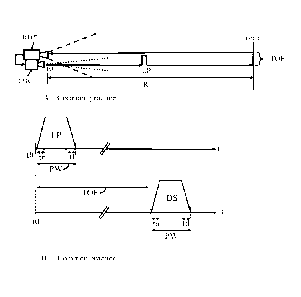
Fig. A illustrates the principles of operation of a commonly used range
measurement
device. Common range finders measure the time of flight TOF, which is the time
taken by a
laser pulse LP emitted towards a target TROT by a lasing device LSR, to hit
the target TROT
and return therefrom to a photo detector DTCT, or detector DTCT for short. The
range R may
3
CA 03178864 2022- 11- 15
WO 2022/009202
PCT/IL2021/050829
then be calculated by multiplying half of the derived time of flight TOF with
the speed of
light.
Evidently, the accuracy of the range measurement depends on the accuracy of
the
measurement of the time of flight TOF.
For this purpose, those common accurate range finders require both, a fast
response
detector having a time constant shorter than a desired time resolution, dt,
which is dependent
on the resolution of the range measurement, and a laser pulse LP having a
narrow pulse width
PW, shown in Fig. B, having the same order of time magnitude as the time
constant T.
Fig. B depicts the time sequence of a short laser pulse LP emitted towards a
target TRGT
and returned therefrom, and the detected analog signal DS derived from the
laser pulse LP by
a fast response photo detector DTCT operative as a common practice range
measurement
device. The time of flight TOF is also shown in Fig. B.
The equation generally used to derive the distance separating a target TRGT
apart from a
range finder is
R = c * TOF/2 (equ. 1)
where R is the range, c is the speed of light and TOF/2 is the time of flight
TOF divided by
two, since the time measured from the time of emission of the laser pulse to
the beginning of
generation of the detector signal DS equals the time taken by light to travel
both ways, to the
target TRGT and back to the detector DTCT.
For example, to obtain a range accuracy measurement of 5m, the required time
resolution dt would be the time light travels 5m forth and back, which is
approximately 33ns.
Therefore, a slow response detector DTCT having a time constant T of less than
lns would be
required to measure the range R with such accuracy. Since many slow response
detectors
DTCT, and specifically slow response thermal detectors THRDTC have time
constants
ranging from a few its to a few ms, it would be advantageous if the same range
measurement
accuracy could be achieved with those slow response detectors DTCT.
Still another problem relates to the capability to use the apparatus APP as a
LIDAR, or
Light Imaging Detection And Ranging device, and to derive 2D thermal images
from the
viewed scenery for their interlacing with the ranges measured by the LIDAR. In
other words,
the capability of the apparatus APP to combine the measured ranges with the 2D
image pixels,
4
CA 03178864 2022- 11- 15
WO 2022/009202
PCT/IL2021/050829
to form a 3D thermal representation, or 3D thermal image, of targeted objects.
A 3D thermal
representation is a mathematical representation of the surfaces and/or the
dimensions of an
object, including the object's length, width, and depth, as well as the
relative temperature
thereof.
Common LIDAR systems use fast response detectors DTCT, either as single
detectors or
in arrays of detectors, and short-pulse lasers LSR to produce 3D
representations. LIDARs
operating in the near infrared region of the optical spectrum are commercially
available, but
do not allow obtaining of 2D thermal images of the viewed scenery in
combination with the
3D imaging of that same scenery.
The data contained in a 2D thermal image, representing the relative
temperatures
between the pixels, and the data contained in a 3D image, representing the
different ranges to
each pixel, complement each other. It would be advantageous for purposes of
advanced image
processing, algorithms and Artificial Intelligence, if both could be
represented interlaced as
one 3D thermal representation or image. An apparatus APP for obtaining such a
3D thermal
representation based on a slow response dual mode thermal detector array, or
bimodal array
BMDARR for short, may further be advantageous for the sake of cost
effectiveness and
simplicity of design.
Solution to Problem
To solve the first problem, a method for measuring a range R by use of a slow-
response
thermal detector THRDTC is now described.
Fig. 1 schematically depicts a graph of amplitude vs. time of a laser pulse LP
emitted at
time t = 0. The amplitude of the laser pulse LP rises through a rise time tr
to a plateau, then
falls through a fall-time tf, and has a pulse width PW which lasts longer in
time than a time
constant r of a slow-response detector THRDTC. The time constant r is not
shown in the Figs.
Fig. 1 further depicts the detected signal DS derived by the slow time
response detector
THRDTC from the laser pule pulse LP emitted toward and returned from the
target TRGT.
Since the detected signal DS starts at the end of the time of flight TOF, the
start time of the
detected signal DS is thus time Tbg. By definition, the time Tbg equals the
time of flight TOF,
i.e. the time taken by a laser pulse LP emitted towards a target TRGT by a
lasing device LSR,
to hit the target TRGT, and return therefrom. Hence:
TOF = Tbg (equ. 2)
5
CA 03178864 2022- 11- 15
WO 2022/009202
PCT/IL2021/050829
As shown in Fig. 1, the detected signal DS ascends exponentially from the end
of the time of
flight TOF, until a time Tpeak at which the maximal intensity of the detected
signal DS is
reached, whereafter the detected signal DS decays exponentially. Reference is
now made to
the sampling of the detected signal DS, and in particular to a method of
asynchronous
sampling.
Fig. 2 illustrates the asynchronous sampling of the detected signal DS, and
Fig. 3 depicts
a particular result of such a sampling process.
By definition, an asynchronous sampling method samples both the ascending
portion ta
and the decaying portion td of the detected signal DS, and sampling proceeds
in sequential and
consecutive amplitude steps of constant and equal amplitude levels AMPLVLi.
In Fig. 2, the amplitude intervals which separate between the levels of
amplitude
AMPLVLi are constant, but not so for the time intervals that separate apart
between the
successive time events of asynchronous sampling. For each one level of
amplitude AMPLVi.
the asynchronous sampling method derives two sampled signals which correspond
to two time
events. A first time event tli for the ascending portion ta of the detected
signal DS, and a
second time event t2i for the decaying portion td of the detected signal DS.
Thus, with an
index i for one same amplitude level AMPLVLi, and an index j = 1 for the
occurrence of the
time event during the ascending portion and an index j = 2 for the decaying
portion of the
sampled detected signal DS, the amplitude level may be marked as AMPLVLi, and
the
asynchronous time samplings as tji. The index i is an integer ranging from 1
to n, and the
index j is either 1 or 2. In Fig. 2 for example, for the amplitude level with
i = 3, or AMPLVL3.
the corresponding values of time events tji are t13 and t23.
Fig. 3 clearly shows that the amplitude intervals which separate between the
levels of
amplitude AMPLVLi are constant, whereas the distance which separates apart
between two
time events tji is dependent from the shape of the detected signal DS.
Furthermore, Fig. 3
illustrates a particular case in which the sampled signal SIGSMP has three
different amplitude
levels AMPLVL. In a more general case, a plurality of amplitude levels AMPLVLi
may be
generated, depending on the target's range R, on the target's radiometric
properties, such as
emissivity, and on the amplitude intervals INTVL which separates apart between
the levels of
amplitude AMPLVLi.
6
CA 03178864 2022- 11- 15
WO 2022/009202 PCT/IL2021/050829
The two series of time events, namely tli and t2i, may be used to calculate
the beginning
time Tbg of the detected signal DS shown in Figs. 1, 2, and 3, by use of the
following
equations.
When the rise times tr and the falling times If are about zero or close to
zero, thus for tr
tf 0, the beginning time Tbg of the detector signal DS may be calculated by
use of the
following equation 3:
Tbg = = In (e mitt (epwit 1) = e-12i/t) (equ. 3)
In other cases, the detector signal beginning time Tbg may be calculated by
use of the
following three equations, namely equ. 4.1 to equ. 4.3:
= = - (tli-tr)/ - (PW-tr)/ -
(t2i-PW)/
Tbg = --cln (Cre
(Cf ¨ Cr = e 1-0 = e iT) (equ. 4.1)
Cr = L (1 ¨ e tilt) (equ. 4.2)
tr
Cf = (1 - e-tfit)
(equ. 4.3)
tf
The time Tbg may be calculated either by selection of one pair of times tli
and t2i
corresponding to a specific amplitude level AMPLVLi, or alternatively, by
averaging over
several Tbg time values by use of several time events tli and t2i belonging to
several
amplitude levels AMPLVLi.
The range R to the target TRGT may now be calculated by use of equation 2 and
equation. 5:
R = e * Tbg / 2 (equ. 5)
It is noted that the only variants in the calculation of the range R are the
series of times
events tli and t2i.
It may thus be said in conclusion that a slow-response detector THRDTC, i.e. a
cooled or
an uncooled thermal detector having a relatively slow time response, may be
used for range R
measurement. The precision of the range measurement R depends only on the
accuracy of the
time measurement of the series of time events tli and t2i.
Advantageous Effects of Invention
The apparatus APP as described herewith has the technical advantages of using
slow
response detectors, for deriving 3D thermal imaging combining range
measurement and 2D
thermal images. That description is short of disclosing or even hinting at the
many practical
advantages in many fields of use.
7
CA 03178864 2022- 11- 15
WO 2022/009202
PCT/IL2021/050829
Practically, advantages of the apparatus APP include range measurement, and
the
presentation of a scenery in 3D, in combination with selected 2D thermal
images of the
scenery.
Performance of the apparatus APP may be enhanced for specific use by
calibration of
range and of geometrical dimensions measurement, and to relative or absolute
temperature
measurement.
For public health purposes, the apparatus APP collectively recognizes those
individuals
out of a first group of people having a body temperature above an a priori
selected level,
which individuals are personally targeted, located by range, and identified by
measurements of
biometric features. In addition, the apparatus APP recognizes those
individuals who are closer
to individuals of the firstly recognized group by less than a specifically
selected range of
mutual distance of separation, and identifies a second group of individuals as
being in risk of
being infected by the first identified group. Thereby, the apparatus APP
replaces the sequential
testing and identification of ill or contaminated people. For example, in case
of an epidemic,
the apparatus APP enables the automatic designation and identification of
those specific
individuals out of a crowd, that are at risk of being infected by the epidemic
due to their
disregard of minimal mutual separation apart distances. Thereby, quarantining
of those
individuals at risk may prevent the outspread of the epidemic to the
population.
Lifesaving may be realized by the combination of the herewith described triple
technical
achievements with their economic advantages of simplicity of design and low-
cost production.
The application of such a combination of technical features to advanced driver
assistance
systems (ADAS), say for detection and avoidance of people and animals in poor
visibility
conditions, and when handling complex situation hazards for accident
prevention, is thus
available and cost effective relative to present systems.
Lifesaving may also be realized by installing the apparatus APP inside the
cabin of a
vehicle for sensing of the driver's biometrics and for providing a warning to
avoid forgetting
infants in a parked vehicle.
In case of a blaze, the apparatus APP is able to detect people even if hidden
from sight
beyond a wall of flames, and also to recognize their number and their
distance.
8
CA 03178864 2022- 11- 15
WO 2022/009202
PCT/IL2021/050829
In industry for example, with a group of products disposed in the field of
view of the
apparatus APP, products that exceed predetermined threshold dimensional
tolerances and/or
temperature ranges are detected and identified simultaneously instead of by
separate discrete
inspection procedures.
In robotics for example, the apparatus APP may be used as an improved
artificial eye
whereby an accurate 3D image that includes thermal mapping can provide robots
with
additional data thus increasing the accuracy of the surrounding area's image.
The apparatus APP may also be used in cities incorporating advanced
technologies to
improve the inhabitants' experience and well-being, also known as "smart
cities" for
improving a control center's situational awareness, adding 3D Thermal and
Lidar imaging to
existing optical cameras for increased public safety in a cost-effective
manner.
Brief Description of Drawings
In the drawings, like reference characters generally refer to the same parts
throughout the
different views. Also, the drawings are schematic and not to scale, emphasis
instead generally
being placed upon illustrating the principles of the invention. Various non-
limiting
embodiments of the present invention are described with reference to the
following description
of exemplary embodiments, in conjunction with the figures in which:
Fig. A illustrates the principles of operation of a commonly used range
measurement
method,
Fig. B depicts the time sequence of a short laser pulse emitted to and
returned from a
target, as well as the analog signal detected therefrom by a fast response
photo detector, as
used with common practice range measurement methods,
Fig. 1 presents a graph of a laser pulse LP, and a therefrom derived signal DS
as captured
by a slow-response thermal detector THRDTC,
Fig. 2 illustrates the asynchronous sampling which proceeds in constant
amplitude
intervals INTVL of the analog signal produced by the slow-response detector in
response to
the received long laser pulse,
Fig. 3 illustrates an exemplary structure of the signal SIGSMP having three
amplitude
levels AMPLVLi,
9
CA 03178864 2022- 11- 15
WO 2022/009202
PCT/IL2021/050829
Fig. 4 is a block diagram of a main electrical circuit MNCRCT showing
electrical
elements of the apparatus APP which measures range by use of a slow response
thermal
detector THRDTC and by asynchronous sampling,
Fig. 5 illustrates a data storage pattern symmetric about a transition point
TRPNT, for use
with the asynchronous sampling process,
Fig. 6 illustrates a pixel sampling circuit PXSMP,
Fig. 7 depicts a thermal imaging detector array of standard design, referred
to as photo
array PHTARR,
Fig. 8 illustrates a bimodal array BMDARR for thermal imaging and for range
finding,
with emphasis on a selected line i,
Fig. 9 illustrates a block diagram of an exemplary embodiment of the apparatus
APP.
Fig. 10 illustrates a portion of the 2D image generated by bimodal array
BMDARR, and a
scanning pattern of the laser beam LSRBM projected thereon, and
Fig. 11 depicts successive stages of operation of the controller CNTRL of the
apparatus
APP for the generation of 2D thermal images interlaced with 3D images.
Description of Embodiments
The hereinabove described range finding method using a slow-response thermal
detector
THRDTC may be implemented in the apparatus APP.
Fig. 4 is a schematic block diagram of a main electrical circuit MNCRCT
showing
electrical elements of the apparatus APP for range R measurement by use of low-
cost
detectors and of asynchronous sampling, and illustrates the operation thereof.
A low-cost
detector may cost at least one order of magnitude, or even two orders of
magnitude less than
the cost of a commercially available high quality and high-speed detector.
At time t = 0, a start signal STRT is given, which simultaneously initializes
two elements
of the apparatus APP, namely the laser driver LSRDR and the clock CLK, or time
counter
CLK, which starts to count time. The start signal STRT also resets a thereto
coupled interim
memory INTMM. Once initialized by the start signal STRT, the laser driver
LSRDR
commands a thereto coupled lasing device LSR, or laser LSR, to emit a first
laser pulse LP.
This first laser pulse LP is thence sent to the target TRGT and is returned
therefrom to the
apparatus APP. Upon return from the target TROT, the laser pulse LP is
received by a
detector THRDTC, which may be a slow response thermal detector THRDTC.
CA 03178864 2022- 11- 15
WO 2022/009202
PCT/IL2021/050829
In turn, the thermal detector THRDTC converts the light collected from the
laser pulse
LP to an electrical signal referred to as a detected signal DS. The thermal
detector THRDTC
receives the first laser pulse LP from the time of emission thereof, starting
at the time t = Tbg,
until the time of return of the end of that first laser pulse LP at the time t
= TOF + PW, as
illustrated hereinabove in relation to Fig B. As shown in Fig. B, TOF is the
time of flight, PW
is the pulse width, tr is the rise time and tf is the fall time of the laser
pulse LP. The slow
response thermal detector THRDTC may be a single detector THRDTC or else, one
pixel PXL
of a slow response bimodal array BMDARR, which is described hereinbelow. In
response to
the first laser pulse LP, the slow response thermal detector THRDTC outputs a
detected signal
DS to a pre-amplifier PA. The pre-amplifier PA is a common practice pre-
amplifier circuit.
The pre-amplifier PA is used to amplify the detected signal DS to an analog
voltage
signal Vo(t), which in turn, serves as an input to the pixel sampling circuit
PXSMP. The
functionality of the pixel sampling circuit PXSMP is twofold. The first
function of the pixel
sampling circuit PXSMP is to determine and indicate whether the voltage signal
Vo(t) is rising
or is falling. A flag signal marked R/F is set either to LOGIC1 if the voltage
signal Vo(t) is
rising, or to LOGICO if the voltage signal Vo(t) is falling. The second
function of the pixel
sampling circuit PXSMP is to determine whether the signal Vo(t) has reached a
next
amplitude level AMPLVLi. If so, the pixel sampling circuit PXSMP sends a clock
sampling
signal CLKSMP to the interim memory INTMM, which causes the interim memory
INTMM
to save the current readings of the flag signal R/F and of the clock CLK. The
clock CLK is a
standard time counting component having a resolution which is derived from the
required
range measurement resolution.
For example, if the required range resolution is 5m, the time counting
resolution of the
clock CLK should be selected as 33ns, as explained hereinabove with reference
to Fig. A. This
pixel sampling circuit PXSMP, which is coupled to the interim memory INTMM,
runs a
process which creates the two series of time events tli and t2i described
hereinabove with
respect to Figs. 2 and 3. This process creates the two series of time events
tli and t2i for
storage in the interim memory INTMM, wherein for each sampled clock time CLK,
the flag
signal R/F denotes whether the time event belongs to the series tli of the
rising portion of the
sampled signal SIGSMP, or to the series t2i of the falling portion thereof.
The interim memory
11
CA 03178864 2022- 11- 15
WO 2022/009202
PCT/IL2021/050829
INTMM is coupled to a gate G1 which is further coupled to a standard field-
programmable
gate array FPGA, or gate component FPGA for short.
A signal sent by the signal processor SGNPRC, shown in Fig. 8, opens the gate
G1 ,
whereby the two series of time events tli and t2i are forwarded as a data file
TMFL to the gate
component FPGA. The gate component FPGA first locates the transition point
TRPNT in the
data file TMFL by locating the emplacement in the file where the flag signal
R/F changes
from LOGIC1 to LOGICO.
Fig. 5 thus illustrates that the transition point TRPNT is found by searching
the data file
TMFL for that location where the LOGIC1 switches to LOGICO, or the location
where the
LOGICO changes to LOGIC1.
As depicted in Fig. 5, the data file TMFL has a storage pattern which is
symmetrical
about the transition point TRPNT of the series of time events tli and t2i.
Hence, the two time
events ti 1 and t21 closest to the transition point TRPNT, on either side
thereof, belong to the
maximum amplitude level AMPLVL1. The next two second time events disposed in
symmetry about the transition point TRPNT belong to the next amplitude level
AMPLVL2,
and so forth. These pairs of time events, tli and t2i, are then used by the
gate component
FPGA together with the equations 3, the equations 4.1 to 4.3, and the
equation. 5, to calculate
the time Tbg of the detected signal DS and the range to the target TRGT, as
described
hereinabove with respect to Figs. 1 and 3. The implementation in the gate
component FPGA
of these equations, namely equations 3, 4.1 to 4.3, and 5, is common
engineering practice. The
other parameters required for the calculation of the range R, including the
width PW of the
laser pulse LP, the rise time tr, and the fall time tf, the time constant t of
the detector, and the
speed of light c, are either system constants or physical constants, which may
be stored a
priori, in a memory of the gate component during assembly in factory.
Pixel Sampling Circuit Implementation
An exemplary schematic embodiment of a pixel sampling circuit PXSMP is
illustrated in
Fig. 6.
At a first stage in Fig. 6, a first comparator COMP1 computes the
instantaneous
difference between the analog amplified voltage signal Vo(t) received from the
preamplifier
12
CA 03178864 2022- 11- 15
WO 2022/009202
PCT/IL2021/050829
PA, as depicted in Fig. 4, and an immediately previous amplitude level
AMPLVLi. For the
first sample of the sampling process, the first sampling amplitude AMPLVLi is
set to zero.
Thereafter, at a second stage, a pair of comparators, namely a second
comparator
COMP2 and a third comparator COMP3, which are coupled to the first comparator
COMP1,
receive the output of the first comparator COMP1, and compare the
instantaneous difference
of the output of the first comparator COMP1 with a positive and a negative
constant voltage.
respectively +INTVL and -INTVL. When the instantaneous difference between the
signal
Vo(t) and the amplitude level AMPLVLi equals +INTVL, the output of the
comparator
COMP2 rises to a voltage level defined as LOGIC1, hence indicating a rise of
the voltage
Vo(t) by an amplitude level in comparison to the previous amplitude level
AMPLVLi. When
the instantaneous difference between the signals Vo(t) and the amplitude level
AMPLVLi
equals -INTVL, the output of the third comparator COMP3 rises to a voltage
level defined as
LOGIC1, hence indicating a decay of the voltage Vo(t) by an amplitude level in
comparison to
the previous amplitude level AMPLVLi. Thus, the output of the second
comparator COMP2
may serve as the output flag signal R/F of the pixel sampling circuit PXSMP,
as explained
hereinabove in reference to Fig 4.
Next, at a third stage, a logic XOR gate LXOR, receives the output of the pair
of
comparators, namely the second comparator COMP2 and the third comparator COMP3
of the
second stage. If the output of either one of both the second comparator COPM2
or the third
comparator COPM3 is set to LOGIC1, but not the output of both of them
together, the logic
XOR gate LXOR will produce a second logic output clock sampling signal CLKSMP.
The
second logic output clock sampling signal CLKSMP will save the current
readings of the flag
signal R/F and of the clock CLK to the interim memory INTMM as explained
hereinabove
with reference to Fig. 4. In addition, when the clock sampling signal CLKSMP
is LOGIC1, a
standard sample and hold circuit SMPHOL, coupled to the output of the logic
XOR gate
LXOR, will sample the current value of the signal Vo(t). This last current
value of the signal
Vo(t) will be accepted as the new immediately previous amplitude level
AMPLVLi, as a
reference for a next iteration of the pixel sampling circuit PXSMP. A standard
delay line DL is
used to delay the input of this new amplitude level AMPLVLi to the first stage
comparator
COMP1, so as to avoid the occurrence of a possible internal collision due to
the asynchronous
nature of this process.
13
CA 03178864 2022- 11- 15
WO 2022/009202
PCT/IL2021/050829
Imaging Detector Implementation
Fig. 7 illustrates an exemplary schematic embodiment of a standard design of a
slow
response thermal imaging photo detector array PHTARR, or for short, photo
array PHTARR.
Fig. 7 shows a portion of two arbitrary lines of pixels PXLij of the thermal
imaging photo
array PHTARR, namely lines LN0Ai and LN0Ai+1. Each one pixel PXLij in these
two lines
includes a photo-detector which is composed of a material that is sensitive to
incident light in
the thermal wavelengths of the light spectrum. A read-out electronic circuit
ROTC
implemented in the substrate of the photo array PHTARR contains gates, which
couples the
pixels PXL into lines and the lines into a frame, separately for each line and
separately for the
entire photo array PHTARR. The entirety of the electronics is referred to for
short as the
integrated circuit ROIC. The main purpose of this integrated circuit ROTC is
to transform the
signals of the thermal photo array PHTARR into amplified voltage signals, and
to transmit
these amplified voltage signals synchronously in a standard international
video format.
The thermal photo array PHTARR is composed of materials which are sensitive to
thermal wavelengths. A few examples of such materials which are slow-
responding and are
also suitable for uncooled imaging include PbSe. V0x, and Amorphous Silicon.
Figure 8 illustrates an exemplary schematic embodiment showing how the pixel
sampling circuit PXSMP described hereinabove in relation to Figs. 6, may be
incorporated
into a standard slow response bimodal array BMDARR. This bimodal array BMDARR
may
perform either standard thermal imaging or asynchronous pixel sampling for
range finding
purposes as described in relation with Fig 4.
In Fig. 8, the line LN0Ai depicts an exemplary embodiment of one arbitrarily
selected
line i of the bimodal array BMDARR, thus one line LN0Ai, out of the plurality
of lines
LNOA of the bimodal array BMDARR.
In Fig. 8, each one pixel PXLij of the bimodal array BMDARR includes a thermal
detector THRDTC, and a pre-amplifier PA, which may be used either for standard
imaging
purposes, or for range finding. The selected mode of operation into which the
pixels PXLij of
the bimodal array BMDARR is set, either imaging or ranging, is commanded by
the mode
switch PXMOD, and is received from an external source as described hereinbelow
in relation
to Figs. 9 and 11. When the mode of operation of the mode switch PXMOD is
selected as a
LOGIC , the output signal of the preamplifier PA will be connected directly to
the output of
14
CA 03178864 2022- 11- 15
WO 2022/009202
PCT/IL2021/050829
the bimodal array BMDARR for standard imaging. However, when the selected mode
of
operation of the mode switch PXMOD is selected as a LOGIC1, the output signal
of the
preamplifier PA will be connected to a pixel sampling circuit PXSMP for range
finding, as
described in relation to Fig. 6. The simplicity of the pixel sampling circuit
PXSMP allows the
implementation thereof to be included in each pixel PXLij.
In turn, the pixels PXL of the line LN0Ai are connected, via gates, to the
output of the
integrated circuit ROIC, in the same manner as for the standardly used imaging
mode. Other
components depicted in Fig. 4, namely including the interim memory INTMM, the
clock.
CLK, and the gate component FPGA, are assembled on the signal processor
SGNPRC, which
is different and separate from the bimodal array BMDARR.
Alternatively, some of these components may be implemented as a portion of the
bimodal
array BMDARR.
3D Thermal Imaging Implementation
As illustrated in Fig 9, the apparatus APP includes a thermal imager Cl, or
camera Cl,
which utilizes the bimodal array BMDARR and a signal processor SGNPRC. The
signal
processor SGNPRC includes a clock CLK, an interim memory INTMM, and a field-
programmable gate component FPGA, as depicted in Fig. 8. The apparatus APP
further
includes a laser LSR which is controlled by a laser driver LSRDR. The laser
LSR emits a laser
beam LSRBM at a wavelength to which the bimodal array BMDARR is sensitive, and
has a
beam divergence much narrower than the field of view FOV of the camera Cl.
Additional components of the apparatus APP include an optical scanner OPTSCN,
and a
controller CNTRL which operates the apparatus APP and different components
thereof.
The optical scanner OPTSCN directs the laser beam LSRBM onto selected areas of
the
scenery viewed by the camera Cl. It is assumed that according to common
engineering
practice, the optical scanner OPTSCN is aligned with the camera Cl. It is
further assumed that
the controller CNTRL, which is coupled to the camera Cl and to the optical
scanner
OPTSCN, may direct the laser beam LSRBM to a specifically selected area of the
scenery
viewed by the camera Cl. This may be achieved by commanding the optical
scanner OPTSCN
to shift to a specifically predefined angle of scan. That is to say that, an
area selected in the
CA 03178864 2022- 11- 15
WO 2022/009202
PCT/IL2021/050829
field of view FOV of the camera Cl may be uniquely mapped by one specific
angle of scan of
the optical scanner OPTSCN.
Fig. 10 illustrates an exemplary sequence of operation of the controller CNTRL
of the
apparatus APP, which may be implemented to generate a 3D imaging interlaced
with a 2D
image. For the sake of clarity of description, it is accepted that the bimodal
array BMDARR
has 100 x 100 pixels PXLij, that is, 100 lines LNOA of 100 pixels PXL each. It
is also
accepted that the apparatus APP generates images at a rate of 0.1HZ, which is
equivalent to a
time sequence of 10s.
At a first stage STG1 of operation, the controller CNTRL operates the bimodal
array
BMDARR to generate a 2D thermal image of a selected portion of the scenery.
For this
purpose, the bimodal array BMDARR is set by the controller CNTRL to an imaging
mode by
commanding operation of the mode switch PXMOD to a LOGICO which is sent to the
pixels
of the bimodal array BMDARR. Thereafter a 2D image is captured by use of a
common
standard method and is transmitted by the slow response bimodal array BMDARR
to the gate
component FPGA which is included in the signal processor SGNPRC, as depicted
in Fig 8.
With the present example, the extent of time required for capturing and
transmitting the 2D
image, indicated as "capture" and "transmit" in Fig. 10, is 3.4ms. This extent
of time is based
on the assumption of a 3ms exposure time of the bimodal array BMDARR to the
scenery,
followed by a 400us reading time of the pixel values and the transmission time
of these values
to the gate component FPGA.
At a second stage of operation STG2, following the previous first stage STG1,
the
controller CNTRL will operate the following components of the apparatus APP to
generate a
3D image: the bimodal array BMDARR, the laser LSR via the laser driver LSRDR,
the optical
scanner OPTSCN, and the signal processor SGNPRC.
Still at the second stage of operation STG2, Fig. 11 illustrates an exemplary
portion of 21 x 20
pixels out of the 2D image generated by the bimodal array BMDARR at the first
stage STG1.
Further in Fig. 11, a scanning pattern of the laser beam LSRBM which is
projected on the
bimodal array BMDARR is indicated by an arrow marked A. In this present
example, it is
assumed that the width of the laser beam LSRBM is such that, when reflected
from the
16
CA 03178864 2022- 11- 15
WO 2022/009202
PCT/IL2021/050829
scenery, or from the target TROT and back to the camera Cl, two pixels of the
bimodal array
BMDARR are illuminated at each instantaneous time.
The controller CNTRL commands the laser beam LSRBM to scan that portion of the
selected
scenery viewed by the camera Cl, two pixels PXLij at a time, by adjusting the
angle of
scanning of the optical scanner OPTSCN according to a specific scanning
pattern.
As a first step, the controller CNTRL, shown in Fig. 9, begins by setting the
scanning
pattern, thus the angle of scan of the optical scanner OPTSCN, to illuminate a
first set SET1 of
two pixels PXLij. In Fig. 11, the first set SET1 is disposed in the uppermost
row, at the top of
the first and the second columns, respectively LN0A1 and LN0A2.Thereafter, the
controller
CNTRL commands the first set SET1 to enter the range finding mode, by setting
the mode
switch PXMOD to a LOGIC"1". At a second step, the controller CNTRL starts the
range
finding process by sending a start command to the clock CLK and to the interim
memory
INTMM of the signal processor SGNPRC, and to the laser driver LSRDR. This is
followed by
the process described hereinabove with reference to Figs. 4 to 6. In this
present example, the
duration of this entire process is 2ms.
Next, at the third stage STG3, the controller CNTRL emits a signal which opens
the gate
Gl, shown in Fig. 4, to deliver the file TMFL to the gate component FPGA for
processing. In
response thereto, the gate component FPGA calculates the range to the portion
of the scenery
related to the first set of pixels SET1, as described in relation to Fig. 11.
In parallel, the
controller CNTRL shifts the optical scanner OPTSC to illuminate a second set
SET2 of two
pixels PXL which is disposed in the second row, immediately underneath and
adjacent the
first set SET1, after which the range finding process for these two pixels PXL
of SET2 is
repeated. This range finding process is further repeated iteratively until the
laser beam
LSRBM reaches the end of the first two lines, respectively LN0A1 and LN0A2, on
the
lowermost row.
Thereafter, the laser beam LSRBM will be directed by the controller CNTRL to
the first
two pixels of the next two lines, respectively LN0A3 and LN0A4. This same
scanning
pattern will be repeated iteratively until the laser beam LSRBM completes the
scanning of the
entire portion of the scenery, thereby generating ranges to each and every
pixel PXLij of that
portion of the scenery. In this present example, the duration of time is
approximately lOs for
the entire operation of the bimodal array BMDARR. Adding the duration of the
2D image
17
CA 03178864 2022- 11- 15
WO 2022/009202
PCT/IL2021/050829
generation, which is 3.4ms, to the entire duration of the image generation,
results in 10s,
which is in correlation with the requirement for a rate of 0.1HZ.
It should be noted that the various numerical examples provided herewith are
presented
for the sake of illustration, and are far from exhibiting the best obtainable
performance
achievable by operation of the apparatus APP. At a final stage, the gate
component FPGA
interlaces the thermal 2D image, stored in the memory thereof in pixel format,
with the range
data, by adding the range data of each pixel PXL to the stored 2D thermal
image data. Thereby
a 3D thermal representation of the scenery is created.
The result of the three stages STG of operation of the controller CNTRL is the
capability
to operate the 3D thermal imager Cl for imaging the scenery captured in the
field of view
thereof, to measure a range to selected objects in that field of view, and to
interlace the 2D
thermal image with the range data to generate 3D thermal imaging combining
range with 2D
thermal images.
It is noted that although not depicted as such in the drawings, other
exemplary
embodiments may operate differently, meaning that the sequence of operation of
the described
stages may be different, and so may be the number of instantaneously
illuminated pixels, and
the scanning pattern.
There has thus been described an imaging apparatus APP comprising a 3D thermal
imager Cl, a signal processor SGNPRC, a laser LSR, an optical scanner OPTSCN,
and a
controller CNTRL.
A characteristic of the apparatus, according to exemplary embodiments, is the
use of
slow-response thermal detectors for 3D imaging with high range resolution.
Slow-response
detectors are commonly available and are advantageously priced. The apparatus
combines 2D
thermal images with range data and creates 3D thermal imaging therefrom.
The apparatus APP comprises a bimodal array BMDARR, which is an electronic
circuit
that operates a plurality of slow response thermal detectors THRDTC. In use,
the bimodal
array BMDARR performs either standard thermal imaging, or asynchronous pixel
sampling
for range finding. The bimodal array is commanded by the controller and
includes a plurality
of slow response thermal detectors. Furthermore, the bimodal array is designed
to produce a
2D thermal image as well as accurate range data by use of the slow response
thermal
18
CA 03178864 2022- 11- 15
WO 2022/009202
PCT/IL2021/050829
detectors. Both the 2D thermal image, collected by each slow response thermal
detector in the
array, and the range data, are forwarded to the signal processor.
The controller is further configured to operate the laser, the optical
scanner, and each one slow
response thermal detectors of the thermal imager. Thereby, the controller is
able to operate the
laser, the optical scanner, and the thermal detectors of the thermal imager to
derive therefrom
range data. That range data is collected by use of a pixel sampling circuit
which is dedicated to
derive a plurality of couples of time events tli and t2i. Those couples of
time events tli and t2i
are derived from a sampled detected signal DS which is communicated to the
signal processor.
Finally, the signal processor is configured to compute the range with a degree
of
accuracy superior to the accuracy corresponding to the slow response thermal
detectors in the
array. Thereby, the signal processor is able to interlace the 2D thermal image
with the range
data, to generate 3D thermal imaging combining the range data with the 2D
thermal images.
It is noted that the bimodal array includes a plurality of slow response
thermal detectors,
and that each one of those thermal detectors produces one pixel in a 2D
thermal image and/or
in 3D thermal imaging.
Each one of the detectors THRDTC is coupled to a mode switch PXMOD. The mode
switch
PXMOD is configured to set the bimodal array BMDARR in one of two modes of
operation,
i.e. one mode of operation which is one of an imaging mode, and a second mode
which is a
ranging mode.
The bimodal array BMDARR further comprises a plurality of pixel sampling
circuits
PXSMP. Each one pixel sampling circuit PXSMP is configured to recognize an
ascending
portion ta of a detected signal DS and a decaying portion td of the detected
signal DS.
The signal processor SGNPRC further comprises a clock CLK, and the clock CLK
is coupled
to an interim memory INTMM. The pixel sampling circuits PXSMP is coupled to
the interim
memory INTMM. The pixel sampling circuits PXSMP is configured to send a clock
sampling
signal CLKSMP and a flag signal R/F to the signal processor SGNPRC. In
response to those
two signals, the signal processor SGNPRC commands the interim memory INTMM to
store a
current reading of the clock CLK and of the flag signal R/F.
Each one pixel sampling circuit PXSMP is coupled to the interim memory INTMM,
and
is configured to perform at least two operations. A first operation of the
pixel sampling circuit
19
CA 03178864 2022- 11- 15
WO 2022/009202
PCT/IL2021/050829
PXSMP is to create two series of time events, namely a first series of time
event tli and a
second series of time event t2i. The time events tli belong to an ascending
portion ta of a
detected signal DS and the time events t2i belongs to a decaying portion td of
the same
detected signal DS. The second operation that the pixel sampling circuit PXSMP
performs is
to indicate to which one of both the ascending portion ta and the decaying
portion td each one
of the time event pertains.
The interim memory INTMM is coupled to a component FPGA via a gate G1 .
Opening
of the gate G1 is commanded by the thereto configured signal processor SGNPRC.
Thereby,
the two series of time events tli and t2i which are stored in the interim
memory INTMM may
be forwarded as a data file TMFL to the component FPGA.
The gate component FPGA is configured to locate a transition point TRPNT in
the data
file TMFL. The transition point TRPNT separates apart between the two series
of time events
tli and t2i. To find the transition point TRPNT, it suffices to locate the
emplacement in the
data file TMFL where the flag signal R/F switches from a setting to a LOGIC1
to a setting to a
LOGIC , or vice versa, the emplacement where the flag signal R/F switches from
a setting to
a LOGICO to a setting LOGIC1.
As described hereinabove, the pixel sampling circuit PXSMP is configured to
derive a
plurality of couples of time events tl i and t2i from a sampled detected
signal DS. These
couples of time events tli and t2i may be used to compute a range to a target
TRGT.
The pixel sampling circuit PXSMP is further configured for both: to deliver
the flag
signal R/F and to derive the plurality of couples of time events tli and t21.
Both of these are
collected by asynchronous sampling of the detected signal DS. The detected
signal DS has an
ascending portion ta and a decaying portion td. The flag signal R/F is
configured to indicate to
which one of the ascending portion ta and the decaying portion td each one of
the time events
tli and t2i is related.
The pixel-sampling circuits PXSMP are still further configured to perform at
least two
more operations. One more operation is to asynchronously sample the ascending
portion ta
and the decaying portion td of the sampled detected signal DS. The purpose of
the
asynchronous sampling is to derive the couples of two time events in
sequential steps of
constant and equal spans of interval INTVL and at successive levels of
amplitude AMPLVLi.
CA 03178864 2022- 11- 15
WO 2022/009202
PCT/IL2021/050829
The second operation is to deliver the flag signal R/F for the purpose of
indicating to which
one of the two time events tli and t2i each time event belongs. In turn, a
data file TMFL
containing the couples of time events tli and t2i and the flag signals R/F is
stored in the
interim memory INTMM upon delivery of the clock sampling signal CLKSMP.
Each one couple of the time events tli and t2i includes a first time event tli
and a second
time event t2i. In the first time event tli, the first index is indicated as
1. In the second time
event t2i, the first index is indicated as 2. The first index and the second
index are correlated
with the flag signal R/F. Each one time event tli and t2i is identified by a
second index i. That
second index i is related to an amplitude level AMPLVLij. Each one of the time
events tli and
t2i is saved on an opposite side of a transition point TRPNT having two sides.
The time events
tli are saved in the time file TMFL on a first side of the transition point
TRPNT, and the time
events t2i are saved in the time file TMFL on a second side of the transition
point TRPNT.
Time events having a numerical lower index i are stored closer to the
transition point TRPNT
whereas time events having a numerical higher index i are stored farther away
from the
transition point TRPNT.
The thermal detector THRDTC may be selected as an uncooled detector or as a
cooled
detector.
There has thus also been described a method for constructing and implementing
an
imaging apparatus APP. The imaging apparatus APP comprises a 3D thermal imager
Cl, a
signal processor SGNPRC, a laser LSR, an optical scanner OPTSCN, and a
controller
CNTRL. The method uses a slow response thermal detector THRDCT for deriving a
detected
analog signal DS from an emitted laser pulse LP which is returned from a
target TRGT. The
method asynchronously samples the detected signal DS for deriving therefrom
two series of
time events, respectively tli and t2i. Furthermore, the method derives a time
Tbg by use of
equation (equ. 3), and of equations (equ. 4.1), (equ. 4.2), and (equ. 4.3).
Thereafter, the
method calculates the range R to the target TRGT by use of (equ. 5).
The method uses a thermal detector THRDTC which may be selected either as an
uncooled detector or as a cooled detector.
With the method, the detected signal DS has an ascending portion ta and a
decaying
portion td. The detected signal DS is asynchronously sampled on the thereof
ascending portion
ta, and on the thereof decaying portion td.
21
CA 03178864 2022- 11- 15
WO 2022/009202
PCT/IL2021/050829
Furthermore, the detected signal DS is asynchronously sampled in sequential
and
consecutive amplitude steps of constant and equal amplitude intervals INTVL.
With the method, sampled signals SIGSMP are saved in a time file TMFL. The
sampled
signals SIGSMP are listed in the time file TMFL in a pattern which is
symmetric about a
transition point TRPNT.
The detected signal DS may be amplified to an analog voltage signal Vo(t)
before input into a
pixel sampling circuit PXSMP. The pixel sampling circuit PXSMP has a twofold
functionality.
The detected signal DS is amplified to an analog voltage signal Vo(t) for
input into a pixel
sampling circuit PXSMP. The pixel sampling circuit PXSMP has at least two
functions. A
first function of the pixel sampling circuit PXSMP deals with the
determination and indication
whether the voltage signal Vo(t) is rising or is decaying. A second function
of the pixel
sampling circuit PXSMP deals with the determination whether the signal Vo(t)
has reached a
next amplitude level AMPLVLi or not.
The pixel sampling circuit PXSMP is an element of a main electrical circuit
MNCRCT.
The pixel sampling circuit PXSMP is configured to operate the asynchronous
pixel sampling
process.
The main electrical circuit MNCRCT comprises a standard sample and hold
circuit
SMPHOL. The sample and hold circuit SMPHOL is coupled to a delay line DL. The
delay
line DL and the sample and hold circuit SMPHOL are configured to prevent a
possible
internal collision of derived data.
Industrial Applicability
The exemplary embodiments of the apparatus and the method described
hereinabove are
applicable in industries and appliances using cameras including, for example,
public health,
civil safety and protection, robotics, and guidance and navigation of
vehicles.
22
CA 03178864 2022- 11- 15
WO 2022/009202
PCT/IL2021/050829
List of Reference Items
Name
APP apparatus
BMDARR bimodal array
Cl camera
CLK clock or time counter
CLKSMP clock sampling signal
CNTRL controller
COMP comparator
DL delay line
DS detected signal
DTCT slow response laser pulse detector
FPGA FPGA component
FPGAMM gate component memory
GI gate GI
INTMM interim memory
INTVL amplitude interval
LNOA line of array
LP laser pulse
LSR laser
LSRBM laser beam
LSRDR laser driver
LXOR logic XOR gate
MNCRCT main electrical circuit
OPTCOM optical components
OPTSCN optical scanner
PA preamplifier
PHTARR photo array
PXL pixel
PXMOD mode switch
PXSMPL pixel sampling circuit
range
R/F output flag
ROIC read-out integrated circuit
SGNPRC signal processor
SIGSMP sampled signal
SLRDCT slow response thermal detector
STRT start signal
TID thermal imaging device
THRARR thermal imaging detector array
THRDCT slow response thermal photo detector TC
TMFL data file
Tpealc time of maximal intensity
TRGT target
23
CA 03178864 2022- 11- 15