Note : Les descriptions sont présentées dans la langue officielle dans laquelle elles ont été soumises.
WO 2022/005780
PCT/US2021/038125
DEVICES WITII 'FIELD EFFECT TRANSISTORS
CROSS-REFERENCE TO RELATED APPLICATIONS
[0001] This application claims priority to U.S.
Provisional Application No.
63/047743, filed July 2, 2020, and U.S. Provisional Application No. 63/200868,
filed March
31, 2021, the content of each of which is incorporated by reference in its
entirety.
BACKGROUND
[0002] Various polynucleotide sequencing techniques
involve performing a large
number of controlled reactions on support surfaces or within predefined
reaction chambers.
The controlled reactions may then be observed or detected, and subsequent
analysis may help
identify properties of the polynucleotide involved in the reaction.
[0003] Some of these polynucleotide sequencing techniques
utilize a nanopore,
which can provide a path for an ionic electrical current. For example, as the
polynucleotide
traverses through the nanopore, it influences the electrical current through
the nanopore. Each
passing nucleotide, or series of nucleotides, that passes through the nanopore
yields a
characteristic electrical current. These characteristic electrical currents of
the traversing
polynucleotide can be recorded to determine the sequence of the
polynucleotide.
[0004] FIG. 1A shows a prior art nanopore sequencing
device 1110 as shown in
PCT publication WO 2019/160925. The prior art nanopore sequencing device 1110
includes
a cis well 1114 associated with a cis electrode 1130, a trans well 1116
associated with a trans
electrode 1134, and a field effect transistor (FET) 1122 positioned between
the cis well 1114
and the trans well 1116. The FET 1122 includes a source 1150, a drain 1152,
and a channel
1154. Below the cis well 1114 is a first cavity 1115 facing the cis well 1114.
The trans well
1116 includes a second cavity 1117. A fluidic tunnel 1121 extends through the
FET 1122 from
the first cavity 1115 to the trans well 1116. An electrolyte 1120 is disposed
in the cis well
1114, first cavity 1115 and trans well 1116.
[0005] Between the cis well 1114 and first cavity 1115 :is
a nanopore 1118 that is
disposed into a membrane 1124. The nanopore 1118 has first nanoscale opening
1123
1
CA 03182291 2022- 12- 12
WO 2022/005780
PCT/US2021/038125
fluidically and electrically connecting electrolyte from the cis well 14 to
the first cavity 1115.
The first nanoscale opening 1123 has an inner diameter 1123'. As the
polynucleotide 1129
traverses through the first nanoscale opening 1123, the sequence of the
polynucleotide can be
determined by measuring the change in voltage of the FET sensor 1122. A second
nanoscale
opening 1125 within a base substrate 1162' fluidically connects the fluidic
tunnel 1121 and the
second cavity 1117, with the second nanoscale opening 1125 having an inner
diameter 1125'.
[0006] Metallic interconnects 1164' and 1166' are in
electrical communication
with the source 1150 and drain 1152 of the FET 1122. A relatively thick
interlayer dielectric
1168, generally thicker than about 50 nm, surrounds the channel 1154 and upper
and lower
surfaces of the FET sensor 1122 to form the fluidic tunnel 1121. The FET
sensor 1122 is in
electrical communication with the electrolyte 1120 at the boundary 1156 where
the channel
1154 is closest to the fluidic tunnel 1121. As illustrated, the thickness of
the interlayer
dielectric 1168 on top of, or below, the channel 1154 may be about 3 times or
more the
thickness of the channel 1154 of the FET 1122.
SUMMARY
[0007] Provided in examples herein are devices for
sequencing polynucleotides
and methods of using the devices. One example of such a device is a nanopore
device. In
particular, examples include devices having a field effect transistor (ITT)
sensor and a porous
structure.
[0008] The systems, devices, kits, and methods disclosed
herein each have several
aspects, no single one of which is solely responsible for their desirable
attributes. Without
limiting the scope of the claims, some prominent features will now be
discussed briefly.
Numerous other examples are also contemplated, including examples that have
fewer,
additional, and/or different components, steps, features, objects, benefits,
and advantages. The
components, aspects, and steps may also be arranged and ordered differently.
After
considering this discussion, and particularly after reading the section
entitled "Detailed
Description," one will understand how the features of the devices and methods
disclosed herein
provide advantages over other known devices and methods.
2
CA 03182291 2022- 12- 12
WO 2022/005780
PCT/US2021/038125
[0009] One example is a device comprising a middle well
comprising a fluidic
tunnel; a cis well associated with a cis electrode, wherein a first nanoscale
opening is disposed
between the cis well and the middle well; a trans well associated with a trans
electrode, wherein
a second nanoscale opening is disposed between the trans well and the middle
well; and a field
effect transistor (PET) positioned between the first nanoscale opening and the
second
nanoscale opening. In this example, the FET comprises: a source, a drain, and
a channel
connecting the source to the drain, wherein the channel comprises a gate oxide
layer having an
upper surface fluidically exposed to the middle well, wherein the middle well
fluidically
connects the cis well to the trans well. In some embodiments, the fluidic
tunnel extends through
the channel. In alternative embodiments, the fluidic tunnel is offset from
(i.e., does not extend
through) the FET channel.
[0010] Another example is a device comprising a middle
well comprising a fluidic
tunnel; a cis well associated with a cis electrode, wherein a first nanoscale
opening is disposed
between the cis well and the middle well; a trans well associated with a trans
electrode, wherein
a second nanoscale opening is disposed between the trans well and the middle
well; and a field
effect transistor (FET) positioned between the first nanoscale opening and the
second
nanoscale opening, the WI' comprising: a source, a drain, and a channel
connecting the source
to the drain, wherein the channel comprises a gate oxide layer having an upper
surface and a
lower surface, the surfaces fluidically exposed to the middle well, wherein
the middle well
fluidically connects the cis well to the trans well. In some embodiments, the
fluidic tunnel
extends through the channel. In alternative embodiments, the fluidic tunnel is
offset from (i.e.,
does not extend through) the FET channel.
[0011] Yet another example is a device comprising a middle
well comprising a
fluidic tunnel; a cis well associated with a cis electrode, wherein a first
nanoscale opening is
disposed between the cis well and the middle well; a trans well associated
with a trans
electrode, wherein a porous structure is disposed between the trans well and
the middle well;
and a field effect transistor (FET) positioned between the first nanoscale
opening and the
porous structure, the FET comprising: a source, a drain, and a channel
connecting the source
to the drain, wherein the channel comprises a gate oxide layer having an upper
surface
fluidically exposed to the middle well, wherein the middle well fluidically
connects the cis
well to the trans well. In some embodiments, the fluidic tunnel extends
through the FET
3
CA 03182291 2022- 12- 12
WO 2022/005780
PCT/US2021/038125
channel. In alternative embodiments, the fluidic tunnel is offset from (i.e.,
does not extend
through) the PET channel.
[0012] Still another example is a method of using the any
of the aforementioned
devices in method comprising: introducing an electrolyte into each of the cis
well, the trans
well, the middle well and the fluidic tunnel of a device; applying a voltage
bias between the
cis electrode and the trans electrode, wherein an electrical resistance of the
first nanoscale
opening varies in response to an identity of bases in the polynucleotide at
the first nanoscale
opening, and wherein a potential (Vm) of the electrolyte in the fluidic tunnel
varies in response
to the variation in electrical resistance of the first nanoscale opening; and
measuring a response
of the FET as a function of bases in the polynucleotide at the first nanoscale
opening, to identify
the bases in the polynucleotide.
[0013] It is to be understood that any features of the
device and/or of the array
disclosed herein may be combined together in any desirable manner and/or
configuration.
Further, it is to be understood that any features of the method of using the
device may be
combined together in any desirable manner. Moreover, it is to be understood
that any
combination of features of this method and/or of the device and/or of the
array may be used
together, and/or may be combined with any of the examples disclosed herein.
Still further, it
is to be understood that any feature or combination of features of any of the
devices and/or of
the arrays and/or of any of the methods may be combined together in any
desirable manner,
and/or may be combined with any of the examples disclosed herein.
[0014] It should be appreciated that all combinations of
the foregoing concepts and
additional concepts discussed in greater detail below are contemplated as
being part of the
inventive subject matter disclosed herein and may be used to achieve the
benefits and
advantages described herein.
BRIEF DESCRIPTION OF THE DRAWINGS
[0015] Features of examples of the present disclosure will
become apparent by
reference to the following detailed description and drawings, in which like
reference numerals
correspond to similar, though perhaps not identical, components. For the sake
of brevity,
reference numerals or features having a previously described function may or
may not be
described in connection with other drawings in which they appear.
4
CA 03182291 2022- 12- 12
WO 2022/005780
PCT/US2021/038125
[0016] FIG. 1 A is a cross-sectional side view of a prior
art nanopore sequencing
device.
[0017] FIG. 1B shows a schematic circuit diagram of the
electrical resistance
provided by the prior art nanopore sequencing device of FIG. 1A.
[0018] FIG. 2A is a cross-sectional side view of a
nanopore sequencing device
according to one example.
[0019] FIG. 2B is a cross-sectional top view, taken on
line 3-3 of the nanopore
sequencing device of FIG. 2A.
[0020] FIG. 2B' is a cross-sectional top view, taken on
line 3'-3' of the nanopore
sequencing device of FIG. 2A.
[0021] FIG. 3A shows a cross-sectional side view of an
alternate example of a
nanopore sequencing device according to one example.
[0022] FIG. 3R is a cross-sectional top view, taken on
line 3-3 of the nanopore
sequencing device of FIG. 3A and a FET sensor.
[0023] FIG. 3C is a cross-sectional top view, taken on
line 3'-3' of the nanopore
sequencing device of FIG. 3A and a FET sensor.
[0024] FIG. 3D is an alternate example of a cross-
sectional top view, taken on line
3-3 of a nanopore sequencing device similar to FIG. 3A, but with a wider
example of a FET
sensor.
[0025] FIG. 3E is an alternate example of a cross-
sectional top view, taken on line
3'-3' of a nanopore sequencing device similar to FIG. 3A, but with a wider
example of a FET
sensor.
[0026] FIG. 4A is another cross-sectional side view of an
alternate example of a
nanopore sequencing device.
[0027] FIG. 4B is a cross-sectional top view, taken on
line 3-3 of the nanopore
sequencing device of FIG. 4A.
100281 FIG. 4B' is a cross-sectional top view, taken on
line 3'-3' of the nanopore
sequencing device of FIG. 4A.
l00291 FIG. 5A is cross-sectional side view of yet another
alternate example of a
nanopore sequencing device.
CA 03182291 2022- 12- 12
WO 2022/005780
PCT/US2021/038125
[0030] FIG. 5B is a cross-sectional top view, taken on
line 3-3 of the nanopore
sequencing device of FIG. 5A.
[0031] FIG. 5B' is a cross-sectional top view, taken on
line 3'-3' of the nanopore
sequencing device of FIG. 5A.
[0032] FIG. 6 is a cross-sectional side view of another
exemplary alternate example
of a nanopore sequencing device.
[0033] FIG. 7A is a cross-sectional side view of yet
another exemplary alternate
example of a nanopore sequencing device with an offset opening.
[0034] FIG. 78 is a cross-sectional top view, taken on
line 3-3 of the nanopore
sequencing device of FIG. 5A showing the offset opening.
[0035] FIG. 7B' is a cross-sectional top view, taken on
line 3'-3' of the nanopore
sequencing device of FIG. 5A showing the offset opening.
[0036] FIG. 8 is a cross-sectional side view of a further
exemplary alternate
example of a nanopore sequencing device with a vertical field effect
transistor.
[0037] FIG. 9 is a cross-sectional side view of yet
another further exemplary
alternate example of a nanopore sequencing device with a field effect
transistor having a non-
Faradaic metal electrode.
DETAILED DESCRIPTION
[0038] All patents, applications, published applications
and other publications
referred to herein are incorporated herein by reference to the referenced
material and in their
entireties. If a term or phrase is used herein in a way that is contrary to or
otherwise
inconsistent with a definition set forth in the patents, applications,
published applications and
other publications that are herein incorporated by reference, the use herein
prevails over the
definition that is incorporated herein by reference.
[0039] One example relates to a sequencing device that
includes a field effect
transistor (FET) sensor having channel disposed between the source and the
drain of the FET
sensor. While in many instances herein, the sequencing device are described as
nanopore
devices, the devices need not be nanopore devices and other configurations are
possible. In
one example, the channel has an upper surface, a lower surface, or both
exposed to electrolyte
within the device. The exposed upper and/or lower surface of the FET sensor
provides an
6
CA 03182291 2022- 12- 12
WO 2022/005780
PCT/US2021/038125
increased surface area of the FET in electrical contact with the electrolyte
that improves the
sensitivity of the nanopore sequencing device. Moreover, increasing the
surface area of the
FET exposed to the electrolyte was found to reduce the background electrical
noise in the
sensor, thus providing a multi-factor boost to the signal-to-noise ratio (SNR)
when measuring
nucleic acid sequences that come in contact with the nanopore.
[00401 In one example, the nanopore sequencing system
utilizes an FET sensor
built with gate-all-around (GAA) transistors to further increase the signal to
noise ratio of the
device. This GAA technology allows the FET sensor to not only have an upper
surface that is
exposed to electrolyte, but also have a lower surface that is also exposed to
electrolyte. More
information regarding this structure is described below with reference to FIG.
4A. In one
embodiment, one or more gate-all-around transistors of the nanopore sequencing
system may
comprise an upper surface and a lower surface of the source-drain channel
exposed to an
electrolyte as shown in FIGs. 4A, 413 and 411'. In another embodiment, one or
more gate-all-
around transistors of the nanopore sequencing system may comprise an upper
surface and a
lower surface of a plurality of source-drain channels exposed to an
electrolyte as shown in FIG.
6. In yet another embodiment, one or more gate-all-around transistors of the
nanopore
sequencing system may comprise vertical transistors as shown in FIG 8.
[0041] In another example, the FET is not in direct
contact with the electrolyte.
Instead, a non-Faradaic metal electrode as shown in FIG. 9 is exposed to the
electrolyte and
transmits a detected signal to the sensing FET. This configuration allows for
a significant
simplification of the fabrication process and a better compatibility with
conventional
semiconductor process flows.
[0042] In another example, the solid-state nanopore
structure may be replaced with
a porous structure, as discussed in more detail below. Such porous structures
may be more
readily integrated into a semiconductor fabrication process flow.
[00431 As used herein, the term "exposed to electrolyte"
does not necessarily mean
that a component is directly contacting the electrolyte. For example, a FET
sensor or a channel
of a FET sensor that is exposed to electrolyte may comprise a relatively thin
layer of an
insulator between the sensor or channel and the electrolyte. For example, in
one example the
channel portion of the FET sensor located between the source and drain may be
covered by a
relatively thin layer of a gate oxide, for example a thermally grown silicon
dioxide layer, and
7
CA 03182291 2022- 12- 12
WO 2022/005780
PCT/US2021/038125
the channel with its gate oxide is said to be "exposed to electrolyte".
Alternatively, a thin layer
of an insulator may be formed of high-k dielectrics, such as Hf02, A1203,
silicon nitroxides,
Si3N4, TiO2, Ta205, Y203, La203, ZrO2, ZrSiO4, barium strontium titanate, lead
zirconate
titanate, ZrSix0y, or ZrAlx0y. The layer of gate oxide may be about 10 nm in
thickness, or in
other examples, less than about 9, about 8, about 7, about 6, about 5, about
4, about 3, about 2,
or about I run in thickness and still be within examples described herein.
Electrical Operation of a Nanopore Sequencing Device
[0044] Referring now to FIG. 1B, an equivalent circuit
diagram of a nanopore
device, such as a nanopore device illustrated in FIGs. 2-7, is shown. As
electrolyte is
introduced into each of the cis well, the trans well, the middle well, and the
fluidic tunnel. A
voltage difference V is applied between the cis electrode and the trans
electrode. In some
examples, a polynucleotide is driven through a first nanoscale opening of a
first nanopore, e.g.
a protein nanopore. In alternative examples, the polynucleotide does not pass
through the first
nanopore, but tagged nucleotides are incorporated by a polymerase acting on
the
polynucleotide. In certain embodiments, a single-stranded polynucleotide, a
double-stranded
polynucleotide, tags or labels of incorporated nucleotide bases, or other
representatives of the
incorporated nucleotide bases, and any combination thereof may pass through
the first
nanopore. In certain embodiments, tags or labels of incorporated nucleotide
base may be
separated or dissociated from a polynucleotide, and such tags or labels may
pass through the
first nanopore with or without the polynucleotide passing through the first
nanopore. Examples
are not limited to how the polynucleotide communicates with the nanopore to
cause signal
generation in the nanopore sequencing device. An electrical resistance
Rprotein of the first
nanoscale opening varies in response to an identity of bases at the first
nanoscale opening, e.g.,
while a base of the polynucleotide passes through the first nanoscale opening,
or while a tagged
nucleotide is being incorporated by a polyrnerase acting on the
polynucleotide, thus the
different tags of the tagged nucleotides change the resistance of the first
nanoscale opening.
[0045] In an example, a second nanoscale opening of a
second nanopore, e.g., a
solid-state nanopore, has a fixed, or substantially fixed electrical
resistance Rpore. A potential
of the electrolyte in the fluidic tunnel, denoted as the voltage divider point
M in FIG. 1C, varies
in response to the variation in electrical resistance Rprotein of the first
nanoscale opening.
8
CA 03182291 2022- 12- 12
WO 2022/005780
PCT/US2021/038125
Therefore, measuring the response of the FET as the resistance changes in the
first nanoscale
opening permits determination of the resistance in the first nanoscale
opening, and such
information can be used to identify the base in the polynucleotide.
100461 During a nanopore sequencing operation, the
application of the electrical
potential (i.e., voltage difference V) across the first nanopore may force the
translocation of a
nucleotide through the first nanoscale opening along with the anions carrying
charges.
Depending upon the bias, the nucleotide may be transported from the cis well
to middle well,
or from the middle well to the cis well. As the nucleotide transits through
the first nanoscale
opening, the current across the membrane 24 changes due, for example, to base-
dependent
blockage of the constriction, for example. The signal from that change in
current can be
measured using the FET sensor. Examples of measuring the response of the FET
include:
measuring a source drain current; or measuring a potential at the source
and/or drain.
Additionally, a resistance in the FFT channel can be measured to identify the
base at the first
nanoscale opening.
[0047] During operation, the range of measured voltages
can be selected from
about -0.1 V to upwards of about 0.1 V. from about -0.5 V to upwards of about
0.5 V. from
about -1 V to upwards of about I V. from about -1.5 V to upwards of about 1.5
V. from about
-2.0 V to upwards of about 2.0 V, from about -3.0 V to upwards of about 3.0 V,
from about -
5.0 V to upwards of about 5.0 V. The voltage polarity is typically applied
such that the
negatively charged nucleic acid is electrophoretically driven towards the
trans electrode. In
some instances, the voltage can be reduced, or the polarity reversed, to
facilitate appropriate
function of the device. In one non-limiting example, the resistance of the
first nanoscale
opening, Rprotein, may be about 0.5 to about 1 giga-ohm (GS/). The resistance
of the second
nanoscale opening, Rpore, may be about 50 mega-ohm (Na). In one example,
Rorolein changes
as a function of the base of the polynucleotide at the first nanoscale
opening.
[00481 The potential of the voltage divider point M varies
with Rp rotern and acts as
the FET gate potential. The resistance Rpore of the second nanoscale opening,
which may be
formed in a solid-state nanopore, is fixed or at least substantially fixed and
is not modulated
by the base of the polynucleotide at the first nanoscale opening. For example,
as the
polynucleotide enters the constriction of the first nanoscale opening, the
resistance Rprotein of
the first nanoscale opening is modulated based on the identity of the bases in
the
9
CA 03182291 2022- 12- 12
WO 2022/005780
PCT/US2021/038125
polynucleotide. Alternatively, the resistance RI rotein of the first nanoscale
opening is modulated
based on the identity of a tag of a tagged nucleotide that is being
incorporated by a polymerase
acting on the polynucleotide. The resistance &weir: may be relatively large,
and generallu
varies by 30-40% as a function of different polynucleotide bases at the first
nanoscale opening.
In other examples, the resistance Rprotein may vary by between about 0.001% to
about 1%, about
1% to about 5%, about 5% to about 20%, about 20% to about 40%, about 40% to
about about
60%, or 60% to about 100%. The resistance Rpore of the second nanoscale
opening, which may
be have a larger size than the first nanoscale opening, may be about 10 times
lower compared
to Rprotein. Since the function of the second nanoscale opening is to provide
the fixed resistance
Rpore in the voltage divider (but not to read out the current associated with
the first nanoscale
opening), the second nanoscale opening may not need to be atomically precise.
[00491 The equivalent circuit shown in FIG. 1B is a
voltage divider, where the
potential of point M is the potential of the electrolyte in the fluidic
tunnel. This potential is the
equivalent gate potential of the FET and establishes its operating point. As
the potential Vu of
point M changes with base identity of the polynucleotide, the current flowing
through the FET
(the source-drain current) changes, providing a measurement of the current
flowing through
the first nanoscale opening, and therefore of the identity of polynucleotide
base. In certain
embodiments, the equivalent circuit of the nanopore device satisfies the
following equations:
[0050] The potential VA,/ at point M is given by
Vm = DV
(1)
[0051] where
Rprotein
D ¨ n
(2)
npore Rprotein
100521 is the voltage divider ratio and V is the cis-trans
bias.
100531 The signal that drives the PET sensor response is
olfm, the variation of the
potential VA/ as the base of the polynucleotide at the first nanoscale opening
changes. From
the above the following relationship can be derived:
6Vm = 1745D
(3)
[0054] where 5D is the variation in the voltage divider
ratio as the base of the
polynucleotide at the first nanoscale opening changes.
CA 03182291 2022- 12- 12
WO 2022/005780
PCT/US2021/038125
[0055] The signal Slim may exceed the limit of detection
(LoD) of the FET sensor,
i.e., V8D > LoD. Therefore, the sensitivity of the nanopore device 10 improves
as LoD is
reduced, V is increased, or 51) is increased.
[0056] The operating cis-trans bias V may therefore
satisfy:
LoD
V>¨-
(4)
51)
Examples
[0057] One example of a nanopore sequencing device with an
PET sensor having
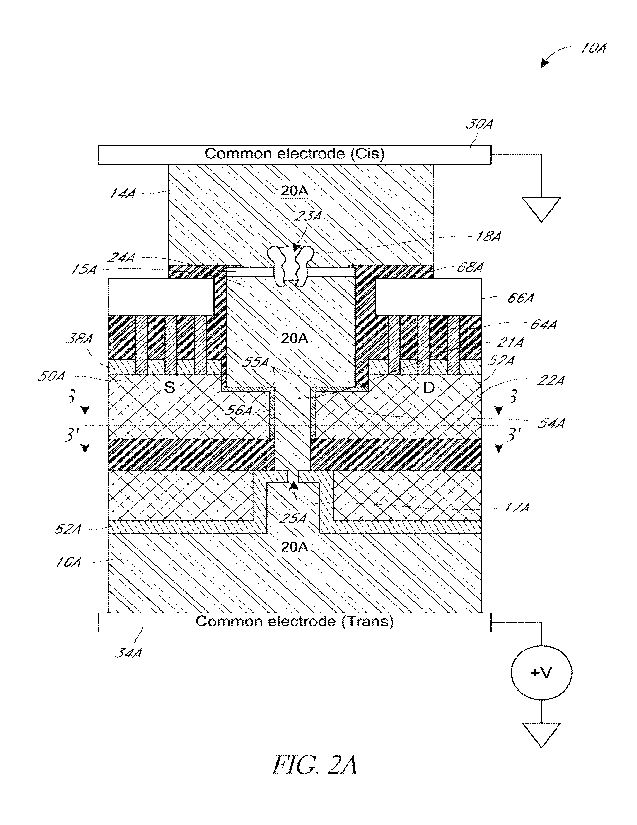
an increased surface area exposed to electrolyte is shown in FIG. 2A. FIG. 2A
is a side cross-
sectional view of the exemplary device 10A. FIG. 2B is a cross-sectional top
view, taken on
line 3-3 of FIG. 2A. FIG. 2B' is a cross-sectional top view, taken on line 3'-
3' of FIG. 2A.
[0058] The nanopore sequencing device 10A shown in FIGs.
2A, 2B, and 2B'
includes a cis electrode 30A connecting to a cis well 14A. The cis well 14A
has a lower portion
that includes a first nanopore 18A. disposed into a membrane 24A. The first
nanopore 1.8A.
includes a first nanoscale opening 23A. defined by the first nanopore 18A.
that communicates
with a fluidic tunnel 21A to a second nanoscale opening 25A disposed in a
narrower region
17A between the fluidic tunnel 21A and a trans well 16A at a lower portion of
the device 1.0A.
As shown, the second nanoscale opening is formed in the substrate material
62A. The first
nanopore 18A provides a fluidic pathway for electrolyte 20A to pass between
the cis well 14A
and the middle well 15A. The fluidic tunnel 21A provides a fluidic pathway for
the electrolyte
to pass from the middle well 15A, through the second nanoscale opening 25A and
to the trans
well 16A.
[0059] In one example, the cis electrode 30A and the trans
electrode 34A are at
least substantially parallel to one another in an at least substantially
horizontal direction. In
other examples, the cis electrode and the trans electrode may be in any
suitable orientation
relative to each other and to the nanopore device. The nanopore device 10A
further includes a
field effect transistor (PET) sensor 22A positioned between the first
nanoscale opening 23A
and the second nanoscale opening 25A. The PET sensor includes a source (S)
50A, a drain
(D) 52A, and a channel 54A that connects the source 50A to the drain 52A. As
shown in top
views, FIGS. 2B and 2B', the electrolyte 20A can be seen in the fluidic tunnel
21A and
extending through the channel 54A. Metallic interconnects 64A and 66A are in
electrical
11
CA 03182291 2022- 12- 12
WO 2022/005780
PCT/US2021/038125
communication with the source 50A and drain 52A of the FET 22A, through the
etch stop layer
38A. The metallic interconnects 64A and 66A communicate data from the FET
sensor 22A to
a control system monitoring the FET sensor 22A.
[00601
In the example of the nanopore device 10A shown in FIG. 2A, a thin layer
of gate oxide 56A is grown around the channel MA, therefore its upper surface
55A is
fluidically exposed to the electrolyte 20A in the middle well 15A. The gate
oxide 56A may
have a vertical surface fluidically exposed to the electrolyte 20A in the
fluidic tunnel 21A. The
thin layer of gate oxide 56A separates the channel 54A from the electrolyte
20A and exposes
the channel 54A of the FET sensor 22A to the electrolyte 20A. The thickness of
the gate oxide
56A may be between about land about 10 nrn, or alternatively between about
2and about 4
nm. The thickness of the gate oxide 56A is chosen such that a strong enough
electric field,
given the potential V.A4, can induce an inversion layer of electrons, or
holes, which constitute a
conductive path at the boundary of the channel 54A and gate oxide 56A to
provide a
measurable conduction between the source 50A and drain 52A of the FET 22A.
[0061]
In this configuration, the upper surface 55A of the gate oxide 56A of
the
channel 54A fluidically exposes the channel 54A. to the electrolyte in the
middle well 15A., as
shown in FIG. 2B. By providing a large area of the channel MA exposed to the
electrolyte
20A, the potential 14.i has a better gate controllability over the channel
54A.
[0062]
Following equations (2) and (4) above, assuming that the expected level
separation in R prot ein-1 0% of the open pore resistance, with an expected
base divider ratio
D-0.1, then the variation 8D-0.1x0.1 = 0.01. Using a FET sensor with a 3 nic4/
.1,0D implies
0.003V
V > ¨ 0.3V .(5)
0.01
[00631
Such high cis-trans bias V may be incompatible with some choices of the
membrane 24A.
[00641
Reduction of the LAO to about 0.2 mV reduces the required cis-trans bias
V
by about 15x (15 times), to about 20 mV, which is compatible with typical
membranes. This
means FET sensors with large gate areas would be advantageous. In the FET
sensor as shown
in prior art FIG. 1A, only a small fraction of the channel 1154 is exposed to
the variation in
voltage 8Vm, mainly through the gate oxide 56A at the boundary of the fluidic
tunnel 21A. In
addition to exposing the channel 54A to the variation in voltage through the
boundary of the
12
CA 03182291 2022- 12- 12
WO 2022/005780
PCT/US2021/038125
fluidic tunnel 21A, the structure with the exposed upper surface 55A as shown
in FlGs. 2A,
2B and 2B' greatly increases the sensing area of the FET exposed to 81/m and
improves the
Loa which scales as 1/sqrt(A), where A is the area of the channel 54A exposed
to the
electrolyte 20A.
[0065] The interlayer dielectric 68A may be any suitable
insulator, including SiO2,
I-1f02, or Al2O3. When the interlayer dielectric 68A is silicon dioxide,
etching may be
performed to etch the various components of the nanopore sequencing device.
For example,
etching may be performed using an etchant with high anisotropy, such as
fluorinated reactive
ion etch including CHF3/02, C2F6, C3Fs, and C5F8/C0/02/Ar as some non-limiting
examples.
[0066] The membrane 24A may be any of the non-permeable or
semi-permeable
materials. The first nanoscale opening 23A extends through the membrane 24A.
It is to be
understood that the membrane 24A may be formed from any suitable natural or
synthetic
material, as described herein. In an example, the membrane 24A is selected
from the group
consisting of a lipid and a biomimetic equivalent of a lipid. In a further
example, the membrane
24A is a synthetic membrane (e.g., a solid-state membrane, one example of
which is silicon
nitride), and the first nanoscale opening 23A is in a solid-state nanopore
extending through the
membrane 24A. In an example, the first nanoscale opening 23A extends through,
for example:
a polynucleotide nanopore; a polypeptide nanopore; or a solid-state nanopore,
e.g., a carbon
nanotube, disposed in the membrane.
[0067] In one example, the source, drain, and channel of
the FET sensor 22A may
be formed of silicon, and a surface of the silicon may be thermally oxidized
to form a gate
oxide on the channel of the FET sensor 22A.
[0068] The first nanopore 18A may be any of the biological
nanopores, e.g., a
protein nanopore, solid-state nanopores, hybrid nanopores, e.g., a hybrid
protein/solid state
nanopore, and synthetic nanopores. In some examples, the nanopore has two open
ends and a
hollow core or hole (i.e., the first nanoscale opening) that connects the two
open ends. When
inserted into the membrane, one of the open ends of the nanopore faces the cis
well and the
other of the open ends of the nanopore faces the middle well. In some
instances, the open end
of the nanopore that faces the middle well is fluidically connected to the
fluidic tunnel and may
also be aligned with at least a portion of the fluidic tunnel. In other
instances, the open end of
the nanopore that facf.es the middle well is fluidically connected to the
fluidic tunnel, but is not
13
CA 03182291 2022- 12- 12
WO 2022/005780
PCT/US2021/038125
aligned with the fluidic tunnel. The hollow core of the nanopore enables the
fluidic and
electrical connection between the cis well and the middle well. The diameter
of the hollow
core of the nanopore may range from about 1 nm up to about 1 gm, and may vary
along the
length of the nanopore. In some examples, the open end that faces the cis well
may be larger
than the open end that faces the middle well. In other examples, the open end
that faces the
cis well may be smaller than the open end that faces the middle well.
[0069] The first nanopore 18A may be inserted into the
membrane directly, or the
membrane may be formed around the nanopore. In an example, the nanopore may
insert itself
into a formed lipid bilayer membrane. For example, a nanopore in its monomeric
form or
polymeric form (e.g., an octamer) may insert itself into the lipid bilayer and
assemble into a
transmembrane pore. In another example, the nanopore may be added to a
grounded side of a
lipid bilayer at a desirable concentration where it will insert itself into
the lipid bilayer. In still
another example, the lipid bilayer may be formed across an aperture in a
polytetrafluoroethylene (PTFE) film and positioned between the cis well and
the middle well.
The nanopore may be added to the grounded cis compartment, and may insert
itself into the
lipid bilayer at the area where the PTFE aperture is formed. In yet a further
example, the
nanopore may be tethered to a solid support (e.g., silicon, silicon oxide,
quartz, indium tin
oxide, gold, polymer, etc.). A tethering molecule, which may be part of the
nanopore itself or
may be attached to the nanopore, may attach the nanopore to the solid support.
The attachment
via the tethering molecule may be such that a single pore is immobilized
(e.g., between the cis
well and the middle well). A lipid bilayer may then be formed around the
nanopore.
[0070] In an example, the second nanoscale opening inner
diameter is at least about
two times larger than the first nanoscale opening inner diameter. In another
example, the
second nanoscale opening inner diameter is about three times larger than the
first nanoscale
opening inner diameter. In yet another example, the second nanoscale opening
inner diameter
ranges from about two times larger than the first nanoscale opening inner
diameter to about
five times larger than the first nanoscale opening inner diameter. In an
example, the area of
the second nanoscale opening ranges from about five times to about 10 times
larger than the
area of the first nanoscale opening.
[0071] Further, in an example, the first nanoscale opening
inner diameter ranges
from about 0.5 nm to about 3 nm, and the second nanoscale opening inner
diameter 25A ranges
14
CA 03182291 2022- 12- 12
WO 2022/005780
PCT/US2021/038125
from about 10 nm to about 20 nm. In another example, the first nanoscale
opening inner
diameter 23A ranges from about 1 mn to about 2 nm, and the second nanoscale
opening inner
diameter 25A ranges from about 10 nm to about 20 nm. In yet another example,
the first
nanoscale opening inner diameter 23A ranges from about 1 nm to about 3 nm, and
the second
nanoscale opening inner diameter 25A ranges from about 2 nm to about 20 nm.
The example
ranges for the first nanoscale opening inner diameter 23A given above are
intended to be the
smallest diameter of the nanoscale opening 23A through the first nanopore 18A.
[0072] A substrate comprising an array of nanopore
sequencing devices may have
many different layouts of first nanoscale openings on the array, including
regular, repeating,
and non-regular patterns of nanoscale openings. In an example, the first
nanoscale openings
may be disposed in a hexagonal grid for close packing and improved density of
the devices.
Other array layouts may include, for example, rectilinear (i.e., rectangular)
layouts, triangular
layouts, and so forth As examples, the layout or pattern can be an x-y format
of first nanoscale
openings that are in rows and columns. In some other examples, the layout or
pattern can be
a repeating arrangement of first nanoscale openings. In still other examples,
the layout or
pattern can be a random arrangement of first nanoscale openings. The pattern
may include
spots, posts, stripes, swirls, lines, triangles, rectangles, circles, arcs,
checks, plaids, diagonals,
arrows, squares, and/or cross-hatches.
[0073] The layout of nanoscale openings may be
characterized with respect to the
density of first nanoscale openings (i.e., number of first nanoscale openings
in a defined area
of the substrate comprising the array). For example, an array of first
nanoscale openings may
be present at a density ranging from about 10 first nanoscale openings per mm2
to about
1,000,000 first nanoscale openings per mm2. The density may also include, for
example, a
density of at least about 10 per mm2, about 5,000 per mm2, about 10,000 per
mm2, about 0.1
million per mm2, or more. Alternatively or additionally, the density may no
more than about
1,000,000 per mm2, about 0.1 million per mm2, about 10,000 per mm2, about
5,000 per mm2,
or less. It is to be further understood that the density of the first
nanoscale openings in the
substrate can be between one of the lower values and one of the upper values
selected from the
ranges above.
[0074] The layout of first nanoscale openings in an array
on a substrate may also
be characterized in terms of the average pitch, i.e., the spacing from the
center of a first
CA 03182291 2022- 12- 12
WO 2022/005780
PCT/US2021/038125
nanoscale opening to the center of an adjacent first nanoscale opening (center-
to-center
spacing). The pattern can be regular such that the coefficient of variation
around the average
pitch is small, or the pattern can be non-regular in which case the
coefficient of variation can
be relatively large. In an example, the average pitch may range from about 100
nm to about
500 pm. The average pitch can be, for example, at least about 100 nm, about 5
pm, about 10
gm, about 100 gm, or more. Alternatively or additionally, the average pitch
can be, for
example, at most about 500 pm, about 100 pm, about 50 pm, about 10 tun, about
5 tun, or less.
The average pitch for an example array of devices can be between one of the
lower values and
one of the upper values selected from the ranges above. In an example, the
array may have a
pitch (center-to-center spacing) of about 10 pm. In another example, the array
may have a
pitch (center-to-center spacing) of about 5 pm. In yet another example, the
array may have a
pitch (center-to-center spacing) ranging from about 1 um to about 10 tun.
[0075] As mentioned above, a substrate for sequencing may
include an array of
nanopore sequencing devices. In one example of a nanopore sequencing device,
the trans well
is fluidically connected to the cis well by the middle well and the respective
second and first
nanoscale openings. In a substrate with an array of nanopore sequencing
devices, there may
be one common cis well and one common trans well communicating with a portion,
or all, of
the nanopore sequencing devices within the array on the substrate. However, it
should be
understood that an array of the nanopore devices may also include several cis
wells that are
fluidically isolated from one another and are fluidically connected to
respective one or more
tans wells fluidically isolated from one another and defined in the substrate.
Multiple cis wells
may be desirable, for example, in order to enable the measurement of multiple
polynucleotides
on a single substrate. In some embodiments, a substrate with an array of
nanopore sequencing
devices comprises one common cis electrode, one common trans electrode, one
common cis
well, one common trans well, and a plurality of nanopore sequencing devices,
such as those
shown in FIG. 2A where each nanopore sequencing device comprises a FET sensor
and a dual
pore with a first nanopore and a second nanopore. Each nanopore sequencing
device of the
plurality of nanopore sequencing devices can separately measure the resistance
or signal by its
associated FET sensor. In other embodiments, each nanopore sequencing device
may
comprise a multiple pore with three or more nanopores and a FET sensor. in
other
embodiments, the substrate with an array of nanopore sequencing devices
comprises one
16
CA 03182291 2022- 12- 12
WO 2022/005780
PCT/US2021/038125
common cis well, a plurality of trans wells, and a plurality of nanopore
sequencing devices,
where each nanopore sequencing device can be individually addressable with
individual trans
electrodes. In other embodiments, the substrate with an array of nanopore
sequencing devices
comprises a plurality of cis wells, a plurality of trans wells, and a
plurality of nanopore
sequencing devices, where each nanopore sequencing device can be individually
addressable
with individual trans electrodes.
[0076] The cis well of a nanopore sequencing device may be
a fluid chamber that
is defined, by sidewalls that are connected to the substrate. In some
examples, the sidewalls
and the substrate may be integrally formed, such that they are formed from a
continuous piece
of material (e.g., glass or plastic). In other examples, the sidewalls and the
substrate may be
separate components that are coupled to each other. In an example, the
sidewalls are photo
patternable polymers. In some examples, the cis well is formed within the
space defined by
the cis electrode, portions of the substrate, and the membrane. The cis well
may have any
suitable dimensions. In an example, the cis well ranges from about 1 mm x 1 mm
to about 3
cm x 3 cm. The cis electrode, whose interior surface forms one surface of the
cis well, may be
physically connected to the sidewalls. The cis electrode may be physically
connected to the
sidewalls, for example, by an adhesive or another suitable fastening
mechanism. The interface
between the cis electrode and the sidewalls may seal the upper portion of the
cis well.
[0077] The trans well of the nanopore sequencing device is
a fluid chamber that
may be defined in a portion of the substrate. The trans well may extend
through the thickness
of the substrate and may have openings at opposed ends of the substrate. In
some examples, a
trans well may have sidewalls that are defined by the substrate and/or by
interstitial regions of
the substrate, a lower surface that is defined by the trans electrode and an
upper surface that is
defined by a base structure. Thus, the trans well may be formed within the
space defined by
the trans electrode, the other portion and/or interstitial regions of the
substrate, and the base
structure. It is to be understood that the upper surface of the trans well may
include the second
nanoscale opening to provide fluid communication to the middle well. In some
examples, the
second nanoscale opening goes through the base structure. In some examples,
the second
nanoscale opening may be fluidically connected to and facing a narrower region
of the trans
well.
17
CA 03182291 2022- 12- 12
WO 2022/005780
PCT/US2021/038125
[0078] The trans well may be a micro well (having at least
one dimension on the
micron scale, e.g., about 1 p.m up to, but not including, about 1000 p.m) or
nanowells (having
the largest dimension on the nanoscale, e.g., about 10 nm up to, but not
including, 1000 nm).
The trans well may be characterized by its aspect ratio (e.g., width or
diameter divided by depth
or height in this example). In an example, the aspect ratio of the trans well
may range from
about 1:1 to about 1:5. In another example, the aspect ratio of each trans
well may range from
about 1:10 to about 1:50. In an example, the aspect ratio of the trans well is
about 3.3. The
depth/height and width/diameter of the trans well may be selected in order to
obtain a desirable
aspect ratio. The depth/height of each trans well can be at least about 0.1
p.m, about 1 pm,
about 10 gm, about 100 p.m, or more. Alternatively or additionally, the depth
can be at most
about 1,000 pm, about 100 p.m, about 10 pm, about 1 gin, about 0.1 um, or
less. The
width/diameter of each trans well 16 can be at least about 50 nm, about 0.1
p.m, about 0.5 gm,
about 1 p.m, about 10 p.m, about 100 pm, or more. Alternatively or
additionally, the
width/diameter can be at most about 1,000 gm, about 100 tun, about 10 pm,
about 1 p.m, about
0.5 p.m, about 0.1 p.m, about 50 nm, or less.
[0079] The cis well and the trans well may be fabricated
using a variety of
techniques, including, for example, photolithography, nanoimprint lithography,
stamping
techniques, embossing techniques, molding techniques, microetching techniques,
etc. As will
be appreciated by those skilled in the art, the technique used will depend on
the composition
and shape of the substrate and the sidewalls. In an example, the cis well may
be defined by
one or more sidewalls at an end of the substrate, and the trans well may be
defined through the
substrate.
[0080] The trans electrode, whose interior surface is the
lower surface of the trans
well, may be physically connected to the substrate. The trans electrode may be
fabricated in
the process of forming the substrate (e.g., during the formation of the trans
wells).
Microfabrication techniques that may be used to form the substrate and the
trans electrode
include lithography, metal deposition and liftoff, dry and/or spin on film
deposition, etching,
etc. The interface between the trans electrode and the substrate may seal the
lower portion of
the trans well.
[0081] Examples of the material used to form the base
structure 62A include silicon
nitride (Si3N4), silicon carbide (SiC), aluminum oxide (A1203), hafnium oxide
(11f02), and
18
CA 03182291 2022- 12- 12
WO 2022/005780
PCT/US2021/038125
tantalum pentoxide (Ta205). Examples of suitable deposition techniques for
these materials,
in addition to CVD, include atomic layer deposition (ALD), or the like.
Examples of suitable
material combinations for the base structure 62A include Si3N4 , SiO2, SiC or
A1203.
[00821 The cis electrode that is used depends, at least in
part, upon the redox couple
in the electrolyte. As examples, the cis electrode may be gold (Au), platinum
(Pt), carbon (C)
(e.g., graphite, diamond, etc.), palladium (Pd), silver (Ag), copper (Cu), or
the like. In an
example, the cis electrode may be a silver/silver chloride (Ag/AgC1)
electrode. In one
example, the cis well is capable of maintaining the electrolyte in contact
with the first nanoscale
opening. In some examples, the cis well may be in contact with an array of
nanopores, and
thus is capable of maintaining the electrolyte in contact with each of the
nanopores in the array.
[0083] The trans electrode that is used depends, at least
in part, upon the redox
couple in the electrolyte. As examples, the trans electrode may be gold (Au),
platinum (Pt),
carbon (C) (e g., graphite, diamond, etc.), palladium (Pd), silver (Ag),
copper (Cu), or the like.
In an example, the trans electrode may be a silver/silver chloride (Ag/AgC1)
electrode.
[0084] In some examples, the relevant electrochemical half-
reactions at the
electrodes for a Ag/AgCI electrode in NaCl or KCI solution, are:
100851 Cis (cathode): AgCI + e- 4 Ag + Cl and
[0086] Trans (anode): Ai) + Cl 4 AgC1 + e- .
[0087] For every unit charge of current, one Cl atom is
consumed at the trans
electrode. Though the discussion above is in terms of an Ag/AgCI electrode in
NaCI or KCI
solution, it is to be understood that any electrode/electrolyte pair that may
be used to pass the
current may apply.
[0088] In use, an electrolyte may be filled into the cis
well, the middle well, the
fluidic tunnel, the narrower region, and the trans well. In alternative
examples, the electrolyte
in the cis well, the middle well, and the trans well may be different. The
electrolyte may be
any electrolyte that is capable of dissociating into counter ions (a cation
and its associated
anion). As examples, the electrolyte may be an electrolyte that is capable of
dissociating into
a potassium cation (K+) or a sodium cation (Na). This type of electrolyte
includes a potassium
cation and an associated anion, or a sodium cation and an associated anion, or
combinations
thereof. Examples of potassium-containing electrolytes include potassium
chloride (KCl),
potassium ferricyanide (K3[Fe(CN")6] = 31120 or K4Fe(CN)6] = 31h0), or other
potassium-
19
CA 03182291 2022- 12- 12
WO 2022/005780
PCT/US2021/038125
containing electrolytes (e.g., bicarbonate (KHCO.:4) or phosphates (e.g.,
KH2PO4, K2HPO4,
K3PO4). Examples of sodium-containing electrolytes include sodium chloride
(NaCI) or other
sodium-containing electrolytes, such as sodium bicarbonate (NaHCO3), sodium
phosphates
(e.g., Na1-I2PO4, Na2HPO4 or Na3PO4). As another example, the electrolyte may
be any
electrolyte that is capable of dissociating into a ruthenium-containing cation
(e.g., ruthenium
hexamine, such as [Ru(NH3)6]2' or [Ru(NH3)6]31. Electrolytes that are capable
of dissociating
into a lithium cation (Li'), a rubidium cation (RV), a magnesium cation (Me),
or a calcium
cation (Ca') may also be used.
[0099] In examples wherein a plurality of nanopore
sequencing devices forms an
array on a substrate, each of the plurality of the nanopore sequencing devices
in the array may
share a common cis electrode and a common trans electrode. In another example,
each of the
plurality of the nanopore sequencing devices shares a common cis electrode,
but has a distinct
trans electrode. in yet another example, each of the plurality of the nanopore
sequencing
devices has a distinct cis electrode and a distinct trans electrode. In still
another example, each
of the plurality of nanopore sequencing devices has a distinct cis electrode
and shares a
common trans electrode. As the array of nanopore devices is scaled, the volume
of each trans
well typically depletes as the r-Ipower of the well dimension (assuming that a
constant aspect
ratio is maintained). In some example, an anay lifetime is about or above 48
hours, and a
typical diameter of the trans well is about or above 100 p.m.
Alternate Examples
[0090] FIG. 3A shows a variation, of the device 1.0A.
illustrated in FIG. 2A. As
shown in FIG 3A, a nanopore sequencing device 10B includes similar components
with the
device shown in FIG. 2A. However, the substrate material 62B shown in FIG. 3A
does not
have a narrower region as was illustrated in FIG. 2A. The substrate material
62B is more planar
in format.
[0091] The nanopore sequencing device 10B is shown in
FIGs. 3A, 3B, and 3C
includes a cis electrode 30B connecting to a cis well 14B. The cis well I 4B
has a lower portion
that includes a .first nanopore 18B disposed into a membrane 24B. The .first
nanopore I 8B
includes a first nanoscale opening 23B defined by the first nanopore 18B that
communicates
with a fluidic tunnel 21B to a second nanoscale opening 25B between the
fluidic tunnel 21B
and a trans well 16B at a lower portion of the device 10B. As shown, the
second nanoscale
CA 03182291 2022- 12- 12
WO 2022/005780
PCT/US2021/038125
opening 25B is formed in the substrate material 62B. The first nanopore 18B
provides a fluidic
pathway for electrolyte 20B to pass between the cis well 14B and the middle
well 15B. The
fluidic tunnel 21B provides a fluidic pathway for the electrolyte to pass from
the middle well
15B, through the second nanoscale opening 25B and to the trans well 16B. In
use, an
electrolyte may be filled into the cis well 14B, the middle well 15B, and the
trans well 16B.
In alternative examples, the electrolyte in the cis well 14B, the middle well
15B, and the trans
well 16B may be different. In some examples, the diameter of the first
nanoscale opening 23B
may be equal to or smaller than the opening of the fluidic tunnel 21B. A
substrate for
sequencing may include an array of nanopore sequencing devices. In one example
of a
nanopore sequencing device, the trans well is fluidically connected to the cis
well by the middle
well and the respective second and first nanoscale openings. In a substrate
with an array of
nanopore sequencing devices, there may be one common cis well and one common
trans well
communicating with a portion, or all, of the nanopore sequencing devices
within the array on
the substrate. However, it should be understood that an array of the nanopore
devices may
also include several cis wells that are fluidically isolated from one another
and are fluidically
connected to respective one or more trans wells fluidically isolated from one
another and
defined in the substrate. Multiple cis wells may be desirable, for example, in
order to enable
the measurement of multiple polynucleotides on a single substrate. In some
embodiments, a
substrate with an array of nanopore sequencing devices comprises one common
cis electrode,
one common trans electrode, one common cis well, one common trans well, and a
plurality of
nanopore sequencing devices, such as those shown in FIG. 3A where each
nanopore
sequencing device comprises a FET sensor and a dual pore with a first nanopore
and a second
nanopore. Each nanopore sequencing device of the plurality of nanopore
sequencing devices
can separately measure the resistance or signal by its associated FET sensor.
In other
embodiments, each nanopore sequencing device may comprise a multiple pore with
three or
more nanopores and a FET sensor. In other embodiments, the substrate with an
array of
nanopore sequencing devices comprises one common cis well, a plurality of
trans wells, and a
plurality of nanopore sequencing devices, where each nanopore sequencing
device can be
individually addressable with individual trans electrodes. In other
embodiments, the substrate
with an array of nanopore sequencing devices comprises a plurality of cis
wells, a plurality of
21
CA 03182291 2022- 12- 12
WO 2022/005780
PCT/US2021/038125
trans wells, and a plurality of nanopore sequencing devices, where each
nanopore sequencing
device can be individually addressable with individual trans electrodes.
[0092] In one example, the cis electrode 30B and the trans
electrode 34B are at
least substantially parallel to one another in an at least substantially
horizontal direction. In
other examples, the cis electrode and the trans electrode may be in any
suitable orientation
relative to each other and to the nanopore device. The nanopore device 10B
further includes a
field effect transistor (FET) sensor 22B positioned between the first
nanoscale opening 23B
and the second nanoscale opening 25B. The FET sensor includes a source (S)
50B, a drain
(D) 5213, and a channel 54B that connects the source 50B to the drain 52B. As
shown in top
views, FIGs. 3B and 3C, the electrolyte 20B can be seen in the fluidic tunnel
21B and extending
through the channel 54B. Metallic interconnects 64B and 66B are in electrical
communication
with the source 50B and drain 52B of the FET 22B, through the etch stop layer
38B. The
metallic interconnects 6413 and 6613 communicate data from the FFT sensor 2213
to a control
system monitoring the FET sensor 22B.
[0093] In the example of the nanopore device 1013 shown in
FIG. 3A, a thin layer
of gate oxide 5613 is grown around the channel 54B; therefore, its upper
surface 55B is
fluidically exposed to the middle well 15B. The gate oxide 568 may have a
vertical surface
fluidically exposed to the electrolyte 2011 in the fluidic tunnel 218. The
thin layer of gate oxide
separates the channel 54B from the electrolyte 2013 and exposes the channel
54B of the FET
sensor 22B to the electrolyte 20B. In addition to exposing the channel 54B to
the variation in
voltage through the gate oxide 56B at the boundary of the fluidic tunnel 21B,
the structure with
the exposed upper surface 55B as shown in FIGs. 3Aõ 313 and 3C greatly
increases the sensing
area of the FET exposed to (5Vm and improves the LoD. The thickness of the
gate oxide 56B
may be between about 1 and about! 0 nrn in thickness, and in some examples
between about 2
and about 4 nrn in thickness. The thickness of the gate oxide 56B is chosen
such that a strong
enough electric field, given the potential Tim, can induce an inversion layer
of electrons or holes
which constitutes a conductive path at the channel 5413-gate oxide 5613
boundary to conduct
between the source 50B and drain 52B.
[0094] The interlayer dielectric 68B may be any suitable
insulator, including SiO2,
HfO2, or A1203. When the interlayer dielectric 68B is silicon dioxide, etching
may be
performed to etch the various components of the nanopore sequencing device.
For example,
22
CA 03182291 2022- 12- 12
WO 2022/005780
PCT/US2021/038125
etching may be performed using an etchant with high anisotropy, such as
fluorinated reactive
ion etch including HF3/02, C2F6, C3F8, and C3F8/C0/02/Ar as some non-limiting
examples.
[0095] As illustrated, the trans well 16 in FIG. 3A does
not include a narrower
region as compared to FIG. 2A. In some instances, this allows for a larger
trans well I6B. The
basic operating principle remains the same for the remainder of the nanopore
sequencing
device.
[0096] FIG. 3B and FIG. 3C are cross-sectional top views,
taken in FIG. 3A on line
3-3 and line 3'-3', respectively, showing an example of the FET sensor which
is a nanowire
transistor, i.e., the channel 54B has a nanowire configuration.
[0097] In the nanowire transistor, the channel 54B has a
length along a direction
from the source 50B to the drain 52B, a height along a direction from the cis
electrode 30B to
the trans electrode 34B, and a width along a direction at least partially or
substantially
orthogonal to both the length and the height in one example, the length may be
at least about
times the width or the height. The intersection between the fluidic tunnel 21B
and the
channel 5413, in a plane defined by the length and the width, may be disc
shaped as shown in
FIG. 3B and FIG. 3C.
[0098] The Lon of a nanowire transistor having an about
250 nm x 20 nm x 30 nm
nanowire is about 3 mV, while the Loi) of a nanowire transistor having an
about 10,000 rIM X
100 iifn X 30 nm wire is about 0.2 mV.
[0099] FIGs. 3D and FIG. 3E are cross-sectional top views
of a nanosheet FET
sensor 22B', as compared to the nanowire FET sensor 2213 shown in FIGs. 3B and
3C. In the
nanosheet FET sensor 22B', the channel 54B' has a nanosheet configuration. A
thin layer of
gate oxide 56B' separates the upper surface of the channel 54B' from the
electrolyte 20B' and
exposes the channel 54B' of the FET sensor 22B' to the electrolyte 20B'. The
thickness of the
gate oxide 56B' may be about 1- about 10 nm, preferably about 2- about 4 inn.
The thickness
of the gate oxide 56B' is chosen such that a strong enough electric field,
given the potential
Kr, can induce an inversion layer of electrons or holes which constitutes a
conductive path at
the channel 54B'-gate oxide 56B' boundary to conduct between the source 50B'
and drain
52B'. The sensing area of the FET exposed to the electrolyte 20B' is greatly
increased, thus
further improving the LoD.
23
CA 03182291 2022- 12- 12
WO 2022/005780
PCT/US2021/038125
[0100] In the nanosheet VET sensor 22B', the channel 54B'
has a length along a
direction from a source 5013' to a drain 52B', a height along a direction from
the cis electrode
to the trans electrode, and a width along a direction at least partially or
substantially orthogonal
to both the length and the height. The length may be at least about 2 times
the height, and the
width may be at least about 2 times the height. In other examples length may
be at least about
3, about 4, about 5, about 6, about 7, about 8, about 9, about 10 or more
times the height, and
the width may be at least about 3, about 4, about 5, about 6, about 7, about
8, about 9, about
or more times the height. The intersection between the fluidic tunnel 21B' and
the channel
MB', in a plane defined by the length and the width, may be oblong shaped as
shown in FIG.
3D and FIG. 3E (for example, see the oblong shaped boundary of 56B').
[0101] Alternatively, the intersection between the fluidic
tunnel 21B' and the
channel 54B' in a nanosheet transistor can be of nearly arbitrary shape and
size, potentially
increasing the sensing area of the FET even further and thus driving the ton
down even
further. Since the size and shape requirement of the fluidic tunnel may be
relaxed, the
manufacturability of the device may be improved.
Additional Examples
[0102] FIGs. 4A, 4B, and 4B' illustrate another example of
the nanopore device
shown in FIGs. 2A, 2B, and 2B', which uses a gate-all-arround (GAA)
transistor. FIG. 4A is
a cross-sectional side view of a nanopore sequencing device 10C. FIG. 413 is a
cross-sectional
top view, taken on line 3-3 in FIG. 4A.. FIG. 4B' is a cross-sectional top
view, taken on line
3'-3' in FIG. 4A.
[0103] The nanopore sequencing device 10C shown in EEGs.
4A, 4B, and 4B'
includes a cis electrode 30C connecting to a cis well 14C. The cis well 14C
has a lower portion
that includes a first nanopore 18C disposed into a membrane 24C. The first
nanopore 18C
includes a first nanoscale opening 23C defined by the first nanopore 18C that
communicates
with a fluidic tunnel 21C to a second nanoscale opening 25C disposed in a
narrower region
17C between the fluidic tunnel 21C and a trans well 16C at a lower portion of
the device 10C.
As shown, the second nanoscale opening is formed in the substrate material
62C. The first
nanopore 18C provides a fluidic pathway for electrolyte 20C to pass between
the cis well 14C
and the middle well 15C. The fluidic tunnel 21C provides a fluidic pathway for
the electrolyte
to pass from the middle well 15C, through the second nanoscale opening 25C and
to the trans
24
CA 03182291 2022- 12- 12
WO 2022/005780
PCT/US2021/038125
well 16C. A substrate for sequencing may include an array of nanopore
sequencing devices.
In one example of a nanopore sequencing device, the trans well is fluidically
connected to the
cis well by the middle well and the respective second and first nanoscale
openings. In a
substrate with an array of nanopore sequencing devices, there may be one
common cis well
and one common trans well communicating with a portion, or all, of the
nanopore sequencing
devices within the array on the substrate. However, it should be understood
that an array of
the nanopore devices may also include several cis wells that are fluidically
isolated from one
another and are fluidically connected to respective one or more trans wells
fluidically isolated
from one another and defined in the substrate. Multiple cis wells may be
desirable, for
example, in order to enable the measurement of multiple polynucleotides on a
single substrate.
In some embodiments, a substrate with an array of nanopore sequencing devices
comprises
one common cis electrode, one common trans electrode, one common cis well, one
common
trans well, and a plurality of nanopore sequencing devices, such as those
shown in FIG. 4A
where each nanopore sequencing device comprises a FET sensor and a dual pore
with a first
nanopore and a second nanopore. Each nanopore sequencing device of the
plurality of
nanopore sequencing devices can separately measure the resistance or signal by
its associated
FET sensor. In other embodiments, each nanopore sequencing device may comprise
a multiple
pore with three or more nanopores and a FET sensor. In other embodiments, the
substrate with
an array of nanopore sequencing devices comprises one common cis well, a
plurality of trans
wells, and a plurality of nanopore sequencing devices, where each nanopore
sequencing device
can be individually addressable with individual trans electrodes. In other
embodiments, the
substrate with an array of nanopore sequencing devices comprises a plurality
of cis wells, a
plurality of trans wells, and a plurality of nanopore sequencing devices,
where each nanopore
sequencing device can be individually addressable with individual trans
electrodes.
[0104] In one example, the cis electrode 30C and the trans
electrode 34C are at
least substantially parallel to one another in an at least substantially
horizontal direction. In
other examples, the cis electrode and the trans electrode may be in any
suitable orientation
relative to each other and to the nanopore device. The nanopore device 10C
further includes a
field effect transistor (FET) sensor 22C positioned between the first
nanoscale opening 23C
and the second nanoscale opening 25C. The FET sensor includes a source (S)
50C, a drain
(D) 52C, and a channel 54C that connects the source 50C to the drain 52C. As
shown in top
CA 03182291 2022- 12- 12
WO 2022/005780
PCT/US2021/038125
views, FIGs. 4B and 4B', the electrolyte 20C can be seen in the fluidic tunnel
21C and
extending through the channel 54C. Metallic interconnects 66C and 64C are in
electrical
communication with the source 50C and drain 52C of the FET 22C, through the
etch stop layer
38C. The metallic interconnects communicate data from the FET sensor 22C to a
control
system monitoring the FET sensor 22C.
[01051 In the nanopore sequencing device 10C shown in
:FIG. 4A, the bulk of the
material right above line 3-3 separating the channel 54C from the electrolyte
20C is removed,
exposing the channel 54C of the FET sensor 22C to the electrolyte 20C. In
addition, the bulk
of the material right below the channel 54C is removed, or hollowed out,
exposing the channel
54C to the electrolyte from below as well¨this may be formed by undercutting
the active area
MC of the FET sensor 22C by well-known methods. Only a thin layer of gate
oxide 56C is
grown around the channel 54C. An upper surface 55C and a lower surface 58C of
the gate
oxide 56C are fluidically exposed to the electrolyte 20C in the middle well
15C and fluidic
channel 21C. The gate oxide 56C may have a vertical surface fluidically
exposed to the
electrolyte 20C in the fluidic. tunnel 21C. The thin layer of gate oxide 56C
separates the channel
54C from the electrolyte 20C and exposes the channel 54C of the FET sensor 22C
to the
electrolyte 20C. The thickness of the gate oxide 56C may be between about 1
and about 10
nm, and in some examples between about 2 and about 4 nm. The thickness of the
gate oxide
56C is chosen such that a strong enough electric field, given the potential
VA1, can induce an
inversion layer of electrons or holes which constitutes a conductive path at
the channel 54C-
gate oxide 56C boundary to conduct between the source 50C and drain 52C.
[0106] Such a configuration of the FET sensor 22C shown in
FIG. 4A allows the
exposure of a relatively large area of the channel 54C to the electrolyte 20C
(as compared to
FIG. 2A). The channel 54C therefore uses the upper surface 55C and lower
surface 58C for
fluidical.ly connecting the channel 54C to the middle well 15C. Therefore, the
potential Vm
has advantageous gate controllability over the channel 54C, and further
reduces the 1,0D. In
addition to exposing the channel 54C to the variation in voltage through the
gate oxide 56C at
the boundary of the fluidic tunnel 21C, the structure of the FET sensor 22C
with the exposed
upper surface 55C and lower surface 58C as shown in FIGs. 4A, 4B and
4B'greatly increases
the sensing area of the FET exposed to Slim and improves the LoD.
26
CA 03182291 2022- 12- 12
WO 2022/005780
PCT/US2021/038125
[0107] The interlayer dielectric 68C may be any suitable
insulator, such as SiO2,
Hf02 or A1203. When the interlayer dielectric 68C is silicon dioxide, etching
may be
performed to etch the various components of the nanopore sequencing device.
For example,
etching may be performed using an etchant with high anisotropy, such as
fluorinated reactive
ion etch including CHF3/02, C2F6, C3Fg, and C3F8/C0/02/Ar as some non-limiting
examples.
[01081 The membrane 24C may be any of the non-permeable or
semi-permeable
materials. The first nanoscale opening 23C extends through the membrane 24C.
It is to be
understood that the membrane 24C may be formed from any suitable natural or
synthetic
material, as described herein. In an example, the membrane 24C is selected
from the group
consisting of a lipid and a biomimetic equivalent of a lipid. In a further
example, the membrane
24C is a synthetic membrane (e.g., a solid-state membrane, one example of
which is silicon
nitride), and the first nanoscale opening 23C is in a solid-state nanopore
extending through the
membrane 24C In an example, the first nanoscale opening 23C extends through,
for example:
a polynucleotide nanopore; a polypeptide nanopore; or a solid-state nanopore,
e.g., a carbon
nanotube, disposed in the membrane.
[0109] In one example, the source, drain, and channel of
the FET sensor 22C may
be formed of silicon, and a surface of the silicon may be thermally oxidized
to form a gate
oxide on the channel of the PET sensor 22C.
[0110] The first nanopore 18C may be any of the biological
nanopores, solid-state
nanopores, hybrid nanopores, and synthetic nanopores. In some examples, the
first nanopore
18C has two open ends and a hollow core or hole (i.e., the first nanoscale
opening 23C) that
connects the two open ends. When inserted into the membrane 24C, one of the
open ends of
the first nanopore I 8C faces the cis well 14C and the other of the open ends
of the first nanopore
I 8C faces the middle well 15C. In some instances, the open end of the first
nanopore 18C that
faces the middle well 15C is fluidically connected to the fluidic tunnel 21C
and may also be
aligned with at least a portion of the fluidic tunnel 21C. In other instances,
the open end of the
first nanopore 18C that faces the middle well 15C is fluidically connected to
the fluidic tunnel
21C, but is not aligned with the fluidic tunnel 21C. The hollow core of the
first nanopore 18C
enables the fluidic and electrical connection between the cis well 14C and the
middle well 15C.
The diameter of the hollow core of the first nanopore 18C may range from about
1 nm up to
about 1 um, and may vary along the length of the first nanopore 18C. In some
examples, the
27
CA 03182291 2022- 12- 12
WO 2022/005780
PCT/US2021/038125
open end that faces the cis well 14C may be larger than the open end that
faces the middle well
15C. In other examples, the open end that faces the cis well 14C may be
smaller than the open
end that faces the middle well 15C.
Further Examples
[0111] FlGs. 5A, 5B, and 5B' illustrate a modification to
the nanopore device
shown in FIGs. 2A, 2B, and 2B', which uses a porous structure 2500D in lieu of
a second
nanoscale opening 25A shown in FIG. 2A. FIG. 5A is a side cross-sectional view
of the
modified exemplary device 10D. FIG. 5B is a cross-sectional top view, taken on
line 3-3 in
FIG. 5A. FIG. 5B' is a cross-sectional top view, taken on line 3'-3' in FIG.
5A.
101121 The nanopore sequencing device 10D shown in F.IGs.
5A, 5B, and 5B'
includes a cis electrode 30D connecting to a cis well 14D. The cis well 14D
has a lower portion
that includes a first nanopore 18D disposed into a membrane 24D. The first
nanopore 18D
includes a first nanoscale opening 23D defined by the first nanopore 18D that
communicates
with a fluidic tunnel 21D to a narrower region 17D of a trans well 161) at a
lower portion of
the device 10D. The first nanopore 1813 provides a fluidic pathway for
electrolyte 2013 to pass
between the cis well 14D and the middle well 15D. The fluidic tunnel 21D
provides a fluidic
pathway for the electrolyte to pass from the middle well 15D to the trans well
16D. A porous
structure 2500D is disposed between the trans well 161) and the middle well
15D. A substrate
for sequencing may include an array of nanopore sequencing devices. In one
example of a
nanopore sequencing device, the trans well is fluidically connected to the cis
well by the middle
well and the respective second and first nanoscale openings. In a substrate
with an array of
nanopore sequencing devices, there may be one common cis well and one common
trans well
communicating with a portion, or all, of the nanopore sequencing devices
within the array on
the substrate. However, it should be understood that an array of the nanopore
devices may
also include several cis wells that are fluidically isolated from one another
and are fluidically
connected to respective one or more trans wells fluidically isolated from one
another and
defined in the substrate. Multiple cis wells may be desirable, for example, in
order to enable
the measurement of multiple polynucleotides on a single substrate. In some
embodiments, a
substrate with an array of nanopore sequencing devices comprises one common
cis electrode,
one COMMon trans electrode, one ckimmoii cis well, one common trans well, and
a plurality of
nanopore sequencing devices, such as those shown in FIG. 5A where each
nanopore
28
CA 03182291 2022- 12- 12
WO 2022/005780
PCT/US2021/038125
sequencing device comprises a FET sensor and a dual pore with a first nanopore
and a second
nanopore. Each nanopore sequencing device of the plurality of nanopore
sequencing devices
can separately measure the resistance or signal by its associated FET sensor.
In other
embodiments, each nanopore sequencing device may comprise a multiple pore with
three or
more nanopores and a FET sensor. In other embodiments, the substrate with an
array of
nanopore sequencing devices comprises one common cis well, a plurality of
trans wells, and a
plurality of nanopore sequencing devices, where each nanopore sequencing
device can be
individually addressable with individual trans electrodes. In other
embodiments, the substrate
with an array of nanopore sequencing devices comprises a plurality of cis
wells, a plurality of
trans wells, and a plurality of nanopore sequencing devices, where each
nanopore sequencing
device can be individually addressable with individual trans electrodes.
[0113] In one example, the cis electrode 30D and the trans
electrode 34D are at
least substantially parallel to one another in an at least substantially
horizontal direction. In
other examples, the cis electrode and the trans electrode may be in any
suitable orientation
relative to each other and to the nanopore device. The nanopore device 10D
further includes a
field effect transistor (FET) sensor 22D positioned between the first
nanoscale opening 23D
and the porous structure 2500D. The FET sensor includes a source (S) 501), a
drain (D) 52D,
and a channel 5413 that connects the source 50D to the drain 5213. As shown in
top views,
FIGs. 5B and 5B', the electrolyte 20D can be seen in the fluidic tunnel 21D
and extending
through the channel 54D. Metallic interconnects 66D and 64D are in electrical
communication
with the source 50D and drain 52D of the FET 22D, through the etch stop layer
381). The
metallic interconnects 66D and 64D communicate data from the FET sensor 22D to
a control
system monitoring the FET sensor 22D.
[0114] In the example of the nanopore device IOD shown in
FIG. 5A, a thin layer
of gate oxide 56D is grown around the channel 54D; therefore, its upper
surface 55D is
fluidically exposed to the middle well. The gate oxide 56D may have a vertical
surface
fluidically exposed to the electrolyte 20D in the fluidic tunnel 21D. The gate
oxide separates
the channel 54D from the electrolyte 20D and exposes the channel 54D of the
FET sensor 22D
to the electrolyte 20D. The thickness of the gate oxide 56D may be between
about 1 and about
nm, and in some examples between about 2 and about 4 inn. 'The thickness of
the gate
oxide 56D is chosen such that a strong enough electric field, given the
potential 144 can induce
29
CA 03182291 2022- 12- 12
WO 2022/005780
PCT/US2021/038125
an inversion layer of electrons or holes which constitutes a conductive path
at the channel 54D-
gate oxide 56D boundary to conduct between the source 50D and drain 52D.
[0115] In this configuration, the channel 54D has an upper
surface fluidically
connecting the channel 54D to the electrolyte in the middle well 15D, as shown
in FIG. 5B.
By increasing the area of the channel 54D exposed to the electrolyte 20D, the
potential Vi has
a better gate controllability over the channel 54D. In addition to exposing
the channel 54D to
the variation in voltage through the gate oxide 56D at the boundary of the
fluidic tunnel 21D,
the structure with the exposed upper surface of the channel 54D as shown in
FIGs. 5A, 5B and
5B'greatly increases the sensing area of the FET exposed to 811fti and
improves the Lon.
[0116] In FIG. 2A, the second nanoscale opening 25A, e.g.,
formed in a solid-state
nanopore, defines part of the operation of the device. Using current
complementary metal¨
oxide¨semiconductor (CMOS)-technologies to make nanopores of less than about
10 nrn may
be a challenge. However, this choice limits the divider ratio D to-0.1, which
in turn reduces
the variation SD when the base of the polynucleotide at the first nanoscale
opening 23 changes,
which in turn drives up the required cis-trans bias V. In certain embodiments,
the equivalent
circuit of the nanopore device satisfies the following equations:
[0117] In the device 10A of FIG 2A, the signal detected by
the PET sensor is
proportional to
al) 1
protein
=
(6)
a Rprotem nproteen Rpore (R )2
protein Rpore
01181 This signal is maximized when
az
a Rporea Rprotein = o,
(7)
[0119] which translates to a requirement that
Rpore = Rprotein.
(8)
[0120] Fabricating a solid-slate nanopore with size and
resistance similar to that of
a protein nanopore remains challenging for current CMOS-based fabrication
technology.
Furthermore, a single solid-state nanopore meeting this requirement may have a
resistance that
varies, since the polynucleotide, e.g., a single-stranded DNA polymer, with a
width of about 1
nm, is expected to significantly alter the resistance if it traverses the
solid-state nanopore that
has an opening of similar width.
CA 03182291 2022- 12- 12
WO 2022/005780
PCT/US2021/038125
[0121]
In contrast, in FIG. 5A, the second nanoscale opening is replaced with a
porous structure 25001), e.g., a nanoporous fit or membrane. The structure and
function of
the frit is similar to that of glass frits used in reference electrodes. The
pores in the frit may be
randomly distributed and may form complicated pathways. The porosity of the
frit is selected
so that it is sufficient to establish electrical continuity across the frit
(i.e., big enough to allow
ionic species from the electrolyte to pass), but small enough so that
significant resistance to
ionic current is established. The resistance of typical fits having a 1 mm2 in
size is on the
order of 1 MO. Therefore, a 100 nm x 100 nm frit may be expected to have a
resistance of >1
TO. Typical frits have pore sizes of about a few nm and thickness of about]
rum Tuning the
porosity and thickness of the frit should allow achieving the desired target
of
Rfrit = Rprotein
(9)
[0122]
There are numerous fabrication compatible materials that may be used for
the frit. low-x dielectrics, such as porous low-x dielectrics (e.g.,
organosilicate glass (SiCOH),
such as porous organosilicate glass (SiCOH)), may be used and fabricated to
have porosities
that can be tuned as high as 50%. Precursors with ring structures such as
cyclomethicone, e.g.,
decamethylcyclopentasiloxane ([(CH3)2SiO]5), are sometimes used to achieve an
intrinsic
porosity of a few percent. Porosities as high as 50% can be achieved from dual-
phase
precursors such as mixtures of DMDS (dimethyl disulfide, CH3SSCH3) and a-
terpenine, where
the a-terpenine phase is removed via thermal treatment. The structure of the
resulting material
can vary from worm-like mesopores arranged in a disorderly fashion to well-
ordered channel-
like arrays, with typical pore size of about a few nm. Ordered porosity with
periods of about
tens of nm has also been demonstrated.
Additional Example
[0123]
FIG. 6 is a cutaway, schematic and partially cross-sectional view of yet
another exemplary nanopore sequencing device 10E. FIG. 6 illustrates a
modification of FIG.
5A, where the FET sensor further improves the SNR and gate controllability by
using a stack
of channels 601.
[01241
The nanopore sequencing device 10E shown in FIG. 6 includes a cis
electrode 30E connecting to a cis well 14E. The cis well 14E has a lower
portion that includes
a first nanopore I SE disposed into a membrane 24E. The first nanopore ISE
includes a first
31
CA 03182291 2022- 12- 12
WO 2022/005780
PCT/US2021/038125
nanoscale opening 23E defined by the first nanopore 18E that communicates with
a fluidic
tunnel 21E to a narrower region 17E of a trans well 16E at a lower portion of
the device 10E.
The first nanopore 18E provides a fluidic pathway for electrolyte 20E to pass
between the cis
well 14E and the middle well 15E. The fluidic tunnel 21E provides a fluidic
pathway for the
electrolyte to pass from the middle well 15E to the trans well 16E. A porous
structure 2500E
is disposed between the trans well 16E and the middle well 15E. A substrate
for sequencing
may include an array of nanopore sequencing devices. In one example of a
nanopore
sequencing device, the trans well is fluidically connected to the cis well by
the middle well and
the respective second and first nanoscale openings. In a substrate with an
array of nanopore
sequencing devices, there may be one common cis well and one common trans well
communicating with a portion, or all, of the nanopore sequencing devices
within the array on
the substrate. However, it should be understood that an array of the nanopore
devices may
also include several cis wells that are fluidically isolated from one another
and are fluidically
connected to respective one or more trans wells fluidically isolated from one
another and
defined in the substrate. Multiple cis wells may be desirable, for example, in
order to enable
the measurement of multiple polynucleotides on a single substrate. In some
embodiments, a
substrate with an array of nanopore sequencing devices comprises one common
cis electrode,
one common trans electrode, one common cis well, one common trans well, and a
plurality of
nanopore sequencing devices, such as those shown in FIG. 6 where each nanopore
sequencing
device comprises a FET sensor and a dual pore with a first nanopore and a
second nanopore.
Each nanopore sequencing device of the plurality of nanopore sequencing
devices can
separately measure the resistance or signal by its associated FET sensor. In
other
embodiments, each nanopore sequencing device may comprise a multiple pore with
three or
more nanopores and a FET sensor. In other embodiments, the substrate with an
array of
nanopore sequencing devices comprises one common cis well, a plurality of
trans wells, and a
plurality of nanopore sequencing devices, where each nanopore sequencing
device can be
individually addressable with individual trans electrodes. In other
embodiments, the substrate
with an array of nanopore sequencing devices comprises a plurality of cis
wells, a plurality of
trans wells, and a plurality of nanopore sequencing devices, where each
nanopore sequencing
device can be individually addressable with individual trans electrodes.
32
CA 03182291 2022- 12- 12
WO 2022/005780
PCT/US2021/038125
[0125] In one example, the cis electrode 30E and the trans
electrode 34E are at least
substantially parallel to one another in an at least substantially horizontal
direction. In other
examples, the cis electrode and the trans electrode may be in any suitable
orientation relative
to each other and to the nanopore device. The nanopore device 10D further
includes a field
effect transistor (FET) sensor 22E positioned between the first nanoscale
opening 23E and the
porous structure 2500E. The FET sensor includes a source (S) 50E, a drain (D)
52E. Metallic
interconnects 66E and 64E are in electrical communication with the source 50E
and drain 52E
of the FET 22E, through the etch stop layer 38E. The metallic interconnects
66E and 64E
communicate data from the FET sensor 22E to a control system monitoring the
FET sensor
22E.
[0126] The FET sensor 22E is modified such that the FET
further includes a stack
of channels 601 that are aligned substantially horizontally and connect the
source 50E to the
drain 52E. In the example of the nanopore device 10E shown in FIG. 5E, a thin
layer of gate
oxide 56E is grown around the stack of channels 601. The thin layer of gate
oxide separates
the channels from the electrolyte 20E and exposes the channels of the FET
sensor 22E to the
electrolyte 20E. The thickness of the gate oxide 56E may be between about I
and about 10
nm, and in some examples between about 2 and about 4 nm. The thickness of the
gate oxide
56E is chosen such that a strong enough electric field, given the potential
14f, can induce an
inversion layer of electrons or holes which constitutes a conductive path at
the channel 54E-
gate oxide 56E boundary to conduct between the source 50E and drain 52E. Each
channel 605
of the plurality of channels therefore has an upper surface 607 and a lower
surface 608 of the
gate oxide fluidically connecting to the middle well 15E. Each channel 605 may
have a vertical
surface fluidically connecting to the fluidic tunnel 21E. The fluidic tunnel
21E extends through
each of the plurality of channels. Therefore, the total FET sensing area can
be increased by
increasing the number of channels in the stack. By increasing the area of the
channels 601
exposed to the electrolyte 20E, the potential I'm has a better gate
controllability over the
channels. This configuration greatly increases the sensing area of the PET
exposed to 8Vm and
improves the LoD.
[0127] The device ME in FIG. 6 includes a porous structure
2500E, e.g., a
nanoporous frit or membrane. However, it should be realized that this example
may also use
a second nanoscale opening, similar to the structure in FIG. 2A. However, in
the example
33
CA 03182291 2022- 12- 12
WO 2022/005780
PCT/US2021/038125
shown in FIG. 6, the structure and function of the frit is similar to that of
glass frits used in
reference electrodes. The porosity of the frit is selected so that it is
sufficient to establish
electrical continuity across the frit (i.e., big enough to allow ionic species
from the electrolyte
to pass), but small enough that diffusion of polymers across it is not
possible. The resistance
of typical fits 1 inm2 in size is on the order of 1 MO, therefore a 100 nm x
100 nm frit may be
expected to have a resistance of >1 M. Typical frits have pore sizes of about
a few nm and
thickness of about 1 nun. Tuning the porosity and thickness of the fit should
allow achieving
the desired target of Rfilr.
[0128] Other aspects and advantages of the disclosure will
become apparent from
this detailed description taken in conjunction with the accompanying drawings
which illustrate,
by way of example, the principles of the disclosure.
[0129] While only certain features of the examples have
been illustrated and
described herein, many modifications and changes will occur to those skilled
in the art. It is,
therefore, to be understood that the appended claims are intended to cover all
such
modifications and changes.
[0130] Various modification and variation of the described
methods and
compositions will be apparent to those skilled in the art without departing
from the scope of
the examples described herein. It should be understood that examples as
claimed should not be
unduly limited to the specific examples disclosed herein. Indeed, various
modifications that
are obvious to those skilled in the relevant fields are intended to be within
the scope of the
following claims.
[0131] Other aspects and advantages of the disclosure will
become apparent from
this detailed description taken in conjunction with the accompanying drawings
which illustrate,
by way of example, the principles of the disclosure.
[0132] While only certain features have been illustrated
and described herein,
many modifications and changes will occur to those skilled in the art. It is,
therefore, to be
understood that the appended claims are intended to cover all such
modifications and changes.
Alternate Examples
[0133] FIGs. 7A, 713, and 713' illustrate another
variation of the nanopore device
shown in FIGs. 2A, 2B, and 2B', which has an alternate arrangement of the
fluidic tunnel with
respect to the field effect transistor. FIG. 7A is a cross-sectional side view
of a nanopore
34
CA 03182291 2022- 12- 12
WO 2022/005780
PCT/US2021/038125
sequencing device 10F. FIG. 7B is a cross-sectional top view, taken on line 3-
3 in FIG. 7A.
FIG. 7B' is a cross-sectional top view, taken on line 3'-3' in FIG. 7A.
[0134] The nanopore sequencing device 1OF shown in FIGs.
7A, 7B, and 7B'
includes a cis electrode 30F connecting to a cis well 14F. The cis well 14F
has a lower portion
that includes a first nanopore 18F disposed into a membrane 24F. The first
nanopore 18F
includes a first nanoscale opening 23F defined by the first nanopore 18F that
communicates
with an offset fluidic tunnel 21F to a second nanoscale opening 25F. The
second nanoscale
opening 25F is disposed in a narrow region 17F between the offset fluidic
tunnel 21F and a
trans well 16F at a lower portion of the device 10F. As shown, the second
nanoscale opening
25F is formed in the substrate material 62F. In other embodiments, the
substrate material 62F
does not have a narrower region, but is more planar in format, similar to the
structure shown
in FIG. 3A.
[0135] The first nanopore 18F provides a fluidic pathway
for electrolyte 20F to
pass between the cis well 14F and the middle well 15F. As shown in FIG. 7B,
the fluidic tunnel
21F is located offset from the central portion of the device and provides a
fluidic pathway for
the electrolyte to pass from the middle well 15F, through the second nanoscale
opening 25F
and to the trans well 16F.
[0136] A substrate for sequencing may include an array of
nanopore sequencing
devices 10F. In one example of a nanopore sequencing device, the trans well is
fluidically
connected to the cis well by the middle well and the respective second and
first nanoscale
openings. In a substrate with an array of nanopore sequencing devices, there
may be one
common cis well and one common trans well communicating with a portion, or
all, of the
nanopore sequencing devices within the array on the substrate. However, it
should be
understood that an array of the nanopore devices may also include several cis
wells that are
fluidically isolated from one another and are fluidically connected to
respective one or more
trans wells fluidically isolated from one another and defined in the
substrate. Multiple cis wells
may be desirable, for example, in order to enable the measurement of multiple
polynucleotides
on a single substrate. In some embodiments, a substrate with an array of
nanopore sequencing
devices comprises one common cis electrode, one common trans electrode, one
common cis
well, one common trans well, and a plurality of nanopore sequencing devices,
such as those
shown in FIG. 7A where each nanopore sequencing device comprises a FET sensor
and a dual
CA 03182291 2022- 12- 12
WO 2022/005780
PCT/US2021/038125
pore with a first nanopore and a second nanopore. Each nanopore sequencing
device of the
plurality of nanopore sequencing devices can separately measure the resistance
or signal by its
associated FET sensor. In other embodiments, each nanopore sequencing device
may
comprise a multiple pore with three or more nanopores and a FET sensor. In
other
embodiments, the substrate with an array of nanopore sequencing devices
comprises one
common cis well, a plurality of trans wells, and a plurality of nanopore
sequencing devices,
where each nanopore sequencing device can be individually addressable with
individual trans
electrodes. In other embodiments, the substrate with an array of nanopore
sequencing devices
comprises a plurality of cis wells, a plurality of trans wells, and a
plurality of nanopore
sequencing devices, where each nanopore sequencing device can be individually
addressable
with individual trans electrodes.
101371 In one example, the cis electrode 30F and the trans
electrode 34F are at least
substantially parallel to one another in an at least substantially horizontal
direction. In other
examples, the cis electrode and the trans electrode may be in any suitable
orientation relative
to each other and to the nanopore device. The nanopore device I OF further
includes a field
effect transistor (ITT) sensor 22F positioned between the first nanoscale
opening 23F and the
second nanoscale opening 25F. The FET sensor includes a source (S) 50F, a
drain (D) 52F,
and a channel 54F that connects the source 50F to the drain 52F. In some
embodiments, the
channel 54F has a n.anowire configuration, similar to the structure shown in
FIGs. 3B and 3C.
In other embodiments, the channel 54F has a nanosheet configuration, similar
to the structure
shown in FIGs. 3D and 3E. Metallic interconnects 66F and 64F are in electrical
communication
with the source 50F and drain 52F of the FET 22F, through the etch stop layer
38F. The
metallic interconnects communicate data from the FET sensor 22F to a control
system
monitoring the FET sensor 22F. In alternative embodiments, the nanopore
sequencing device
10F may use a porous structure in lieu of the second nanoscale opening 25F,
similar to the
structure illustrated in FIG. 5A.
[0138) As shown in the cross-sectional top views FIGs. 7B
and 7B', the fluidic
tunnel 21F is offset from the channel 54F. In other words, the fluidic tunnel
21F does not
extend through the channel 54F, and therefore is not seen in the cross-
sectional side view FIG.
7A. Rather, the fluidic tunnel 21F extends through the interlayer dielectric
68F around the
channel 54F. In FIGs. 713 and 7B', the electrolyte 2OF can be seen in the
fluidic tunnel 21F.
36
CA 03182291 2022- 12- 12
WO 2022/005780
PCT/US2021/038125
The boundary of the fluidic tunnel 21F may be circular shaped as shown in
FIGs. 713 and 7W.
In other embodiments, the boundary of the fluidic tunnel 21F may be oblong
shaped as shown
in FIG. 3D and FIG. 3E. Alternatively, the boundary of the fluidic tunnel 21F
can be of nearly
arbitrary shape and size. In some embodiments, the FET sensor 22F may include
a stack of
channels, similar to the structure illustrated in FIG. 6, but the fluidic
tunnel does not extend
through the stack of channels.
[0139]
One non-limiting benefit of the arrangement of the offset fluidic tunnel
21F
with respect to the channel 54F shown in FIGs. 7A, 7B and 7B' is a simpler
fabrication process
flow. Etching a hole/opening in the channel may disturb the gate oxide of the
device and
require an additional oxide regrowth step. The embodiment as show in FIGs. 7A,
7B and 713'
can avoid etching a hole or opening within the source-drain channel.
101401
The interlayer dielectric 68F may be any suitable insulator, such as
SiO2,
Hf02 or Al2O3. When the interlayer dielectric 68F is silicon dioxide, etching
may be performed
to etch the various components of the nanopore sequencing device. For example,
etching may
be performed using an etchant with high anisotropy, such as fluorinated
reactive ion etch
including CHF3/02, C2F6, CIF's, and C5F5/C0/02/Ar as some non-limiting
examples.
[0141]
In one example, the source, drain, and channel of the FET sensor 22F may
be formed of silicon, and a surface of the silicon may be thermally oxidized
to form a gate
oxide on the channel of the FET sensor 22F.
[0142]
In the nanopore sequencing device 1OF shown in FIG. 7A, the bulk of the
material right above line 3-3 separating the channel 54F from the electrolyte
20F is removed,
exposing the channel 54F of the FET sensor 22F to the electrolyte 20F. As
shown in FIG. 7A,
a portion the channel 54F is exposed to the electrolyte from below. In other
embodiments,
similar to the structure shown in FIG. 4A, the bulk of the material right
below the channel 54F
may be removed, or hollowed out, exposing a larger portion the channel 54F to
the electrolyte
from below
......................................................................... this
may be formed by undercutting the active area 54F of the FET sensor 22F
by well-known methods. Only a thin layer of gate oxide 56F is grown around the
channel 54F.
An upper surface 55F and a lower surface 58F of the gate oxide 56F are
fluidically exposed to
the electrolyte 20F in the middle well 15F. The thin layer of gate oxide 56F
separates the
channel 54F from the electrolyte 20F and exposes the channel 54F of the FET
sensor 22F to
the electrolyte 20F. The thickness of the gate oxide 56F may be between about
1 and about
37
CA 03182291 2022- 12- 12
WO 2022/005780
PCT/US2021/038125
nm, and in some examples between about 2 and about 4 nm. The thickness of the
gate oxide
56F is chosen such that a strong enough electric field, given the potential
VAi, can induce an
inversion layer of electrons or holes which constitutes a conductive path at
the channel 54F-
gate oxide 56F boundary to conduct between the source 50F and drain 52F.
[0143] The membrane 24F may be any of the non-permeable or
semi-permeable
materials. The first nanoscale opening 23F extends through the membrane 24F.
It is to be
understood that the membrane 24F may be formed from any suitable natural or
synthetic
material, as described herein. In an example, the membrane 24F is selected
from the group
consisting of a lipid and a biorni metic equivalent of a lipid. In a further
example, the membrane
24F is a synthetic membrane (e.g., a solid-state membrane, one example of
which is silicon
nitride), and the first nanoscale opening 23F is in a solid-state nanopore
extending through the
membrane 24F. In an example, the first nanoscale opening 23F extends through,
for example:
polynncleotide nanopore; a polypeptide nanopore; or a solid-state nanopore,
e.g., a carbon
nanotube, disposed in the membrane.
[0144] The first nanopore 18F may be any of the biological
nanopores, solid-state
nanopores, hybrid nanopores, and synthetic nanopores. In some examples, the
first nanopore
18F has two open ends and a hollow core or hole (i.e., the first nanoscale
opening 23F) that
connects the two open ends. When inserted into the membrane 24F, one of the
open ends of
the first nanopore I 8F faces the cis well 14F and the other of the open ends
of the first nanopore
I 8F faces the middle well 15F. In some instances, the open end of the first
nanopore 18F that
faces the middle well 15F is fluidically connected to the fluidic tunnel 21F
and may also be
aligned with at least a portion of the offset fluidic tunnel 21F. In other
instances, the open end
of the first nanopore 18F that faces the middle well 15F is fluidically
connected to the fluidic
tunnel 21F, but is not aligned with the offset fluidic tunnel 21F. The hollow
core of the first
nanopore 18F enables the fluidic and electrical connection between the cis
well I 4F and the
middle well 15F. The diameter of the hollow core of the first nanopore 18F may
range from
about 1 nm up to about 1 um, and may vary along the length of the first
nanopore 18F. In
some examples, the open end that faces the cis well 14F may be larger than the
open end that
faces the middle well 15F. In other examples, the open end that faces the cis
well 14F may be
smaller than the open end that faces the middle well 15F.
38
CA 03182291 2022- 12- 12
WO 2022/005780
PCT/US2021/038125
[0145] A method of using the nanopore sequencing device
1OF may include
introducing an electrolyte 20F into each of the cis well 14F, the trans well
16F, the middle well
15F and the fluidic tunnel 21F. After introducing the electrolyte, the method
may include
providing a polynucleotide to be sequenced into the cis well 14F. After
providing the
polynucleotide, the method may include applying a voltage bias between the cis
electrode 30F
and the trans electrode 34F. The voltage bias drives the polynucleotide from
the cis well 14F
to the middle well 15F, through the first nanoscale opening 23F. As the
polynucleotide passes
through the first nanoscale opening 23F, the electrical resistance of the
first nanoscale opening
varies in response to an identity of bases in the polynucleotide at the first
nanoscale opening.
As a result, the potential (VA4 of the electrolyte 20F in the middle well 15F
(or equivalently,
the offset fluidic tunnel 21F) varies with the identity of bases. The
potential (Tim) is effectively
the gate voltage applied to the FET, which modulates the conductivity of the
channel 54F.
Therefore, measurements of the response of the FET can determine the identity
of the bases.
[0146] FIG. 8 illustrates yet another variation of a
nanopore device, which utilizes
a vertical field effect transistor such that the source-drain channel may not
be etched to form a
fluidic tunnel but instead is oriented vertically along a side of the fluidic
path through the
device as explained below. FIG. 8 is a cross-sectional side view of a vertical
FEY nanopore
sequencing device 810G.
[0147] The nanopore sequencing device 810G shown in FIG. 8
includes a cis
electrode 830G connecting to a cis well 814G. The cis well 814 G has a lower
portion that
includes a first nanopore 818G disposed into a membrane 824G. The first
nanopore 818G
includes a first nanoscale opening 823G defined by the first nanopore 818G
that fluidically
communicates with a second nanoscale opening 825G. The second nanoscale
opening 825G
may be disposed in a narrower region 817G of a trans well 816G at a lower
portion of the
device 810G. As shown, the second nanoscale opening is formed in the substrate
material
862G. In other embodiments, the substrate material 862G does not have a
narrower region, but
is more planar in format, similar to the structure shown in FIG. 3A. The first
nanopore 818G
provides a fluidic pathway for electrolyte 820G to pass between the cis well
814G and the
middle well 815G. A substrate for sequencing may include an array of nanopore
sequencing
devices. In one example of a nanopore sequencing device, the trans well is
fluidically
connected to the cis well by the middle well and the respective second and
first nanoscale
39
CA 03182291 2022- 12- 12
WO 2022/005780
PCT/US2021/038125
openings. In a substrate with an array of nanopore sequencing devices, there
may be one
common cis well and one common trans well communicating with a portion, or
all, of the
nanopore sequencing devices within the array on the substrate. However, it
should be
understood that an array of the nanopore devices may also include several cis
wells that are
fluidically isolated from one another and are fluidically connected to
respective one or more
trans wells fluidically isolated from one another and defined in the
substrate. Multiple cis wells
may be desirable, for example, in order to enable the measurement of multiple
polynucleotides
on a single substrate. In some embodiments, a substrate with an array of
nanopore sequencing
devices comprises one common cis electrode, one common trans electrode, one
common cis
well, one common trans well, and a plurality of nanopore sequencing devices,
such as those
shown in FIG. 8 where each nanopore sequencing device comprises a FET sensor
and a dual
pore with a first nanopore and a second nanopore. Each nanopore sequencing
device of the
plurality of nanopore sequencing devices can separately measure the resistance
or signal by its
associated FET sensor. In other embodiments, each nanopore sequencing device
may
comprise a multiple pore with three or more nanopores and a FET sensor. In
other
embodiments, the substrate with an array of nanopore sequencing devices
comprises one
common cis well, a plurality of trans wells, and a plurality of nanopore
sequencing devices,
where each nanopore sequencing device can be individually addressable with
individual trans
electrodes. In other embodiments, the substrate with an array of nanopore
sequencing devices
comprises a plurality of cis wells, a plurality of trans wells, and a
plurality of nanopore
sequencing devices, where each nanopore sequencing device can be individually
addressable
with individual trans electrodes.
[0148] In one example, the cis electrode 830G and the
trans electrode 834G are at
least substantially parallel to one another in an at least substantially
horizontal direction. In
other examples, the cis electrode and the trans electrode may be in any
suitable orientation
relative to each other and to the nanopore device. The nanopore device 810G
further includes
a vertical field effect transistor (FET) sensor positioned between the first
nanoscale opening
823G and the second nanoscale opening 825G. The FET sensor includes a source
(SRC) 850G,
a drain (an) 852G, and a channel that connects the source to the drain. The
FET channel is
along the vertical direction, which is the direction from the cis electrode
830G to the trans
electrode 834G. In some embodiments, the channel has a nanowire configuration,
similar to
CA 03182291 2022- 12- 12
WO 2022/005780
PCT/US2021/038125
the structure shown in FIGs. 3B and 3C. In other embodiments, the channel has
a nanosheet
configuration, similar to the structure shown in FlGs. 313 and 3E. Metallic
interconnects 866G
and 864G are in electrical communication with the source 850G and drain 852G
of the FET.
The metallic interconnects communicate data from the FET sensor to a control
system
monitoring the FET sensor. In alternative embodiments, the nanopore sequencing
device 810G
may use a porous structure in lieu of the second nanoscale opening 825G,
similar to the
structure illustrated in FIG. 5A.
[0149] As shown in FIG. 8, the source 850G, channel, and
drain 852G of the
vertical PET sensor are vertically stacked. The vertical FET is arranged on a
lateral side of the
middle well 815G. In one example, the source, drain, and channel of the FET
sensor may be
formed of silicon, and a surface of the silicon may be thermally oxidized to
form a gate oxide
856G on the channel of the FET sensor. A vertical side surface of the gate
oxide 856G is
fluidically exposed to the electrolyte 820G in the middle well 815G. The thin
layer of gate
oxide 856G separates the channel from the electrolyte 820G and exposes the
channel of the
FET sensor to the electrolyte 820G. The thickness of the gate oxide 856G may
be between
about I and about 10 nm, and in some examples between about 2 and about 4 nm.
The
thickness of the gate oxide 856G is chosen such that a strong enough electric
field, given the
potential Vm, can induce an inversion layer of electrons or holes which
constitutes a conductive
path at the channel-gate oxide boundary to conduct between the source 850G and
drain 852G.
In some embodiments, the FET sensor may include a plurality of vertical source-
drain channels
that are arranged in parallel along a lateral side of the middle well.
[0150] One non-limiting benefit of the vertical FET sensor
is that etching of a
fluidic tunnel through the PET channel may not be required. Etching a
hole/opening in the
channel may disturb the gate oxide of the device and require an additional
oxide regrowth step.
The embodiment as show in FIG. 8 with the vertical FET arranged on a lateral
side of the
middle well 815G can avoid etching a hole or opening within the source-drain
channel.
[0151) The interlayer dielectric 868G may be any suitable
insulator, such as SiO2,
Hf02 or Al2O3. When the interlayer dielectric 868G is silicon dioxide, etching
may be
performed to etch the various components of the nanopore sequencing device.
For example,
etching may be performed using an etchant with high anisotropy, such as
fluorinated reactive
ion etch including CHF3/02, C2F6, C3F8, and C5F8/C0/02/Ar as some non-limiting
examples.
41
CA 03182291 2022- 12- 12
WO 2022/005780
PCT/US2021/038125
[0152] The membrane 824G may be any of the non-permeable
or semi-permeable
materials. The first nanoscale opening 823G extends through the membrane 824G.
It is to be
understood that the membrane 824G may be formed from any suitable natural or
synthetic
material, as described herein. In an example, the membrane 824G is selected
from the group
consisting of a lipid and a biomimetic equivalent of a lipid. In a further
example, the membrane
824G is a synthetic membrane (e.g., a solid-state membrane, one example of
which is silicon
nitride), and the first nanoscale opening 823G is in a solid-state nanopore
extending through
the membrane 824G. In an example, the first nanoscale opening 823G extends
through, for
example: a polynucleotide nanopore; a polypeptide nanopore; or a solid-state
nanopore, e.g., a
carbon nanotube, disposed in the membrane.
[0153] The first nanopore 818G may be any of the
biological nanopores, solid-state
nanopores, hybrid nanopores, and synthetic nanopores. In some examples, the
first nanopore
818(.3 has two open ends and a hollow core or hole (i.e., the first nanoscale
opening 823(3) that
connects the two open ends. When inserted into the membrane 824G, one of the
open ends of
the first nanopore 818G faces the cis well 814G and th.e other of the open
ends of the first
nanopore 818G faces the middle well 8156. The hollow core of the first
nanopore 818G
enables the fluidic and electrical connection between the cis well 814G and
the middle well
815G. The diameter of the hollow core of the first nanopore 818G may range
from about 1
rim up to about 1 gm, and may vary along the length of the first nanopore
8186. In some
examples, the open end that faces the cis well 81.4G may be larger than the
open end that faces
the middle well 815G. In other examples, the open end that faces the cis well
814G may be
smaller than the open end that faces the middle well 815G..
[0154] A method of using the nanopore sequencing device
8106 may include
introducing an electrolyte 820G into each of the cis well 814G, the trans well
816G, and the
middle well 815G. After introducing the electrolyte, the method may include
providing a
polynucleotide to be sequenced into the cis well 8146. After providing the
polynucleotide, the
method may include applying a voltage bias between the cis electrode 8306 and
the trans
electrode 834G. The voltage bias drives the polynucleotide from the cis well
814G to the
middle well 815G, through the first nanoscale opening 823G. As the
polynucleotide passes
through the first nanoscale opening 823G, the electrical resistance of the
first nanoscale
opening varies in response to an identity of bases in the polynucleotide at
the first nanoscale
42
CA 03182291 2022- 12- 12
WO 2022/005780
PCT/US2021/038125
opening. As a result, the potential (I'M) of the electrolyte 820G in the
middle well 815G varies
with the identity of bases. The potential WO is effectively the gate voltage
applied to the FET,
which modulates the conductivity of the FET channel. Therefore, measurements
of the
response of the FET can determine the identity of the bases.
[0155] FIG. 9 illustrates yet another further variation of
a nanopore sequencing
device with a field effect transistor (FET) having a non-Faradaic metal
electrode. In this
embodiment, the FET has a non-Faradaic metal electrode, which includes a metal
structure
that does not participate in the Faradaic processes in the nanopore sequencing
device, i.e., no
electrochemical reaction occurs at the metal structure. The non-Faradaic metal
electrode is
used to detect the electrical potential of the electrolyte in the middle well
and to transmit the
potential as a detected signal to the FET. This design means that the FET can
detect the
potential of the electrolyte but not be exposed to the electrolyte. FIG. 9 is
a cross-sectional side
view of a nanopore sequencing device 91011
[0156] The nanopore sequencing device 910H shown in FIG. 9
includes a cis
electrode 930H connecting to a cis well 914H. The cis well 9I4H has a lower
portion that
includes a first nanopore 91811 disposed into a membrane 92411. The first
nanopore 918H
includes a first nanoscale opening 923H defined by the first nanopore 91 8H
that fluidically
communicates with a second nanoscale opening 925H.. The second nanoscale
opening 92511
may be disposed in a narrower region 91711 of a trans well 91.611 at a lower
portion of the
device 910H. As shown, the second nanoscale opening is formed in the substrate
material
9621-1. In other embodiments, the substrate material 96211 does not have a
narrower region, but
is more planar in format, similar to the structure shown in FIG. 3A. The first
nanopore 9181-1
provides a fluidic pathway for electrolyte 920H to pass between the cis well
914H and the
middle well 9151-1.
[0157] In one example, the cis electrode 93011 and the
trans electrode 934H are at
least substantially parallel to one another in an at least substantially
horizontal direction. In
other examples, the cis electrode and the trans electrode may be in any
suitable orientation
relative to each other and to the nanopore device. The nanopore device 91011
further includes
a field effect transistor (FET) sensor 922H positioned between the first
nanoscale opening
92311 and the second nanoscale opening 92511. The FET sensor 922H includes a
source (SRC)
95011, a drain (DIIN) 95211, and a channel 954H that connects the source 95011
to the drain
43
CA 03182291 2022- 12- 12
WO 2022/005780
PCT/US2021/038125
952H. The FET channel may be along the horizontal direction. In some
embodiments, the FET
channel has a nanowire configuration, similar to the structure shown in FlGs.
3B and 3C. In
other embodiments, the FET channel has a nanosheet configuration, similar to
the structure
shown in FIGs. 313 and 3E. Metallic interconnects 966H and 964H are in
electrical
communication with the source 950H and drain 952H of the FET. The metallic
interconnects
966H and 964H communicate data from the FET sensor to a control system (now
shown) that
is monitoring the FET sensor. In alternative embodiments, the nanopore
sequencing device
910H may use a porous structure in lieu of the second nanoscale opening 925H,
similar to the
structure illustrated in FIG. 5A
[01581 As shown in FIG. 9, the FET sensor 922H is not in
direct contact with the
electrolyte. In one example, the source, drain, and channel of the FET sensor
may be formed
of silicon, and a surface of the silicon may be thermally oxidized to form a
gate oxide 956H
on the channel of the FFT sensor. As shown in FIG. 9, the gate oxide 956H is
not fluidically
exposed to the electrolyte 920H in the middle well 915H. Instead, a non-
Faradaic metal
electrode structure 999H is exposed to the electrolyte. The metal structure
999H is used to
detect the potential VA,/ of the electrolyte in the middle well and to
transmit the detected signal
to the FET. Compared to the size of the middle well which is of the order of a
few p.m, the path
length or a characteristic size of the metal structure 999H. may be about 1
p.m., 2 p.m. 3 p.m. 4
pm, 5 pm, 6 pm, 7 p.m, 8 p.m. 9 p.m, 10 pm, 20 pm, 30 p.m, 40 gm, 50 p.m, 60
pm, 70 um, 80
pm, 90 pm, 100 pm, 110 pm, 120 p.m, 130 gm, 140 pm, 150 p.m, 160 pm, 170 pm,
180 pm,
190 pin, 200 pm, 210 pm, 220 p.m, 230 gm, 240 p.m, 250 pm, 260 pin, 270 pm,
280 pm, 290
p.m, 300 p.m, or any value therebetween.
[0159] The size and shape of the metal structure 999H may
be chosen appropriately
to avoid a high parasitic capacitance in the system. The metal structure 99911
may be made of
non-Faradaic corrosion-resistant metals with respect to the electrolyte. The
metal structure
99911 may be made of platinum, iridium, ruthenium, palladium, tantalum, gold,
or any
combination thereof. No electrochemical reaction may occur at the metal
structure. In some
embodiments, the metal structure 999H may have a cup-shaped portion exposed to
the
electrolyte in order to increase the contact area with the electrolyte. In
some embodiments, the
portion of the metal structure 999H exposed to the electrolyte may include one
or more holes
or openings. In some embodiments, the portion of the metal structure 99911
exposed to the
44
CA 03182291 2022- 12- 12
WO 2022/005780
PCT/US2021/038125
electrolyte may include several parallel fins in order to increase the contact
area with the
electrolyte, where the fins may be partially vertically or horizontally
arranged. Using the metal
structure 99911 to contact the electrolyte allows the FET to be decoupled from
the middle well,
which may be easier to manufacture in some embodiments. Decoupling the size of
the FET
with the size of the middle well also allows a larger FET, which may allow a
higher signal
detection sensitivity and a lower noise level. This configuration also allows
decoupling of the
size of the FET, which determines the limit of signal detection, from the size
of the metal
structure 99911, and thus provides more design flexibility.
[0160] The thickness of the gate oxide 956H may be between
about 1 and about 10
nm, and in some examples between about 2 and about 4 nm. The thickness of the
gate oxide
956H is chosen such that a strong enough electric field, given the potential
14/ in the middle
well, can induce an inversion layer of electrons or holes which constitutes a
conductive path at
the channel-gate oxide boundary to conduct between the source 950H and drain
952H. The
interlayer dielectric 968H may be any suitable insulator, such as SiO2, Hf02
or A1203. When
the interlayer dielectric 968H is silicon dioxide, etching may be performed to
etch the various
components of the nanopore sequencing device. For example, etching may be
performed using
an etchant with high anisotropy, such as fluorinated reactive ion etch
including CH F3/02, C2 F6,
C3F8, and C.5F5/C0/02/Ar as some non-limiting examples.
[0161] The membrane 92411 may be any of the non-permeable
or semi-permeable
materials. The first nanoscale opening 92311 extends through the membrane
924H. It is to be
understood that the membrane 924H may be formed from any suitable natural or
synthetic
material, as described herein. In an example, the membrane 924H is selected
from the group
consisting of a lipid and a biomimetic equivalent of a lipid. In a further
example, the membrane
924H is a synthetic membrane (e.g., a solid-state membrane, one example of
which is silicon
nitride), and the first nanoscale opening 92314 is in a solid-state nanopore
extending through
the membrane 92411. In an example, the first nanoscale opening 92314 extends
through, for
example: a polynucleotide nanopore; a polypeptide nanopore; or a solid-state
nanopore, e.g., a
carbon nanotube, disposed in the membrane. The first nanopore 918H may be any
of the
biological nanopores, solid-state nanopores, hybrid nanopores, and synthetic
nanopores. In
some examples, the first nanopore 918H has two open ends and a hollow core or
hole (i.e., the
first nanoscale opening 92311) that connects the two open ends. When inserted
into the
CA 03182291 2022- 12- 12
WO 2022/005780
PCT/US2021/038125
membrane 924H, one of the open ends of the first nanopore 918H faces the cis
well 914H and
the other of the open ends of the first nanopore 918H faces the middle well
915H. The hollow
core of the first nanopore 918H enables the fluidic and electrical connection
between the cis
well 914H and the middle well 9I5H. The diameter of the hollow core of the
first nanopore
918H may range from about 1 nm up to about 1 pm, and may vary along the length
of the first
nanopore 918H. In some examples, the open end that faces the cis well 914H may
be larger
than the open end that faces the middle well 91511. In other examples, the
open end that faces
the cis well 914H may be smaller than the open end that faces the middle well
915H.
[0162] A method of using the nanopore sequencing device
910H may include
introducing an electrolyte 920H into each of the cis well 914H, the trans well
916H, and the
middle well 915H. After introducing the electrolyte, the method may include
providing a
polynucleotide to be sequenced into the cis well 914H. After providing the
polynucleotide, the
method may include applying a voltage bias between the cis electrode 930H and
the trans
electrode 934H. In some embodiments, the voltage bias may drive the
polynucleotide from the
cis well 914H to the middle well 915H, through the first nanoscale opening
923H. As the
polynucleotide passes through the first nanoscale opening 9231-i, the
electrical resistance of the
first nanoscale opening varies in response to an identity of bases in the
polynucleotide at the
first nanoscale opening. In alternative embodiments, the polynucleotide does
not pass through
the first nanoscale opening, but tags or labels of nucleotides being
incorporated by a
polymerase acting on the polynucleotide may pass through the first nanoscale
opening or may
temporarily reside in the first nanoscale opening. Thus, the electrical
resistance of the first
nanoscale opening varies in response to an identity of the nucleotide being
incorporated, which
is complementary to the identity of a base in the polynucleotide. As a result,
the potential (Vii)
of the electrolyte 9201-I in the middle well 91511 varies with the identities
of bases in the
polynucleotide. The potential (Vi) is effectively the gate voltage applied to
the FET, which
modulates the conductivity of the FET channel. Therefore, measurements of the
response of
the FET can determine the identity of the bases in the polynucleotide.
[0163] A substrate for sequencing may include an array of
nanopore sequencing
devices such as those shown in FIG. 9. In one example of a nanopore sequencing
device, the
trans well is fluidically connected to the cis well by the middle well and the
respective second
and first nanoscale openings. In a substrate with an array of nanopore
sequencing devices,
46
CA 03182291 2022- 12- 12
WO 2022/005780
PCT/US2021/038125
there may be one common cis well and one common trans well communicating with
a portion,
oral!, of the nanopore sequencing devices within the array on the substrate.
However, it should
be understood that an array of the nanopore devices may also include several
cis wells that are
fluidically isolated from one another and are fluidically connected to
respective one or more
trans wells fluidically isolated from one another and defined in the
substrate. Multiple cis wells
may be desirable, for example, in order to enable the measurement of multiple
polynucleotides
on a single substrate. In some embodiments, a substrate with an array of
nanopore sequencing
devices comprises one common cis electrode, one common trans electrode, one
common cis
well, one common trans well, and a plurality of nanopore sequencing devices,
such as those
shown in FIG. 9 where each nanopore sequencing device comprises a PET sensor
and a dual
pore with a first nanopore and a second nanopore. Each nanopore sequencing
device of the
plurality of nanopore sequencing devices can separately measure the resistance
or signal by its
associated FFT sensor. In other embodiments, each nanopore sequencing device
may
comprise a multiple pore with three or more nanopores and a PET sensor. In
other
embodiments, the substrate with an array of nanopore sequencing devices
comprises one
common cis well, a plurality of trans wells, and a plurality of nanopore
sequencing devices,
where each nanopore sequencing device can be individually addressable with
individual trans
electrodes. In other embodiments, the substrate with an array of nanopore
sequencing devices
comprises a plurality of cis wells, a plurality of trans wells, and a
plurality of nanopore
sequencing devices, where each nanopore sequencing device can be individually
addressable
with individual trans electrodes.
Definitions
[0164] All technical and scientific terms used herein have
the same meaning as
commonly understood to one of ordinary skill in the art to which this
disclosure belongs unless
clearly indicated otherwise.
[0165] As used herein, the singular forms "a", "and", and
"the" include plural
referents unless the context clearly dictates otherwise. Thus, for example,
reference to "a
sequence" may include a plurality of such sequences, and so forth.
[0166] The terms comprising, including, containing and
various forms of these
terms are synonymous with each other and are meant to be equally broad.
Moreover, unless
47
CA 03182291 2022- 12- 12
WO 2022/005780
PCT/US2021/038125
explicitly stated to the contrary, examples comprising, including, or having
an element or a
plurality of elements having a particular property may include additional
elements, whether or
not the additional elements have that property.
[0167] As used herein, the terms "fluidically connecting,"
"fluid communication,"
"fluidically coupled," and the like refer to two spatial regions being
connected together such
that a liquid or gas may flow between the two spatial regions. For example, a
cis well/wells
may be fluidically connected to a trans well/wells by way of a middle well, a
fluidic tunnel,
and a narrower region, such that at least a portion of an electrolyte may flow
between the
connected wells. The two spatial regions may be in fluid communication through
first and
second nanoscale openings, or through one or more valves, restrictors, or
other fluidic
components that are to control or regulate a flow of fluid through a system.
[0168] As used herein, the term "interstitial region"
refers to an area in a
substrate/solid support or a membrane, or an area on a surface that separates
other areas,
regions, features associated with the support or membrane or surface. For
example, an
interstitial region of a membrane can separate one nanopore of an array from
another nanopore
of the array. For another example, an interstitial region of a substrate can
separate one trans
well from another trans well. The two areas that are separated from each other
can be discrete,
i.e., lacking physical contact with each other. In many examples, the
interstitial region is
continuous whereas the areas are discrete, for example, as is the case for a
plurality of
nanopores defined in an otherwise continuous membrane, or for a plurality of
wells defined in
an otherwise continuous substrate/support. The separation provided by an
interstitial region
can be partial or full separation. Interstitial regions may have a surface
material that differs
from the surface material of the features defined in the surface. For example,
the surface
material at the interstitial regions may be a lipid material, and a nanopore
formed in the lipid
material can have an amount or concentration of polypeptide that exceeds the
amount or
concentration present at the interstitial regions. In some examples, the
polypeptide may not be
present at the interstitial regions.
[0169] As used herein, the term "membrane" refers to a non-
permeable or semi-
permeable barrier or other sheet that separates two liquid/gel chambers (e.g.,
a cis well and a
fluidic cavity) which can contain the same compositions or different
compositions therein. The
permeability of the membrane to any given species depends upon the nature of
the membrane.
48
CA 03182291 2022- 12- 12
WO 2022/005780
PCT/US2021/038125
In some examples, the membrane may be non-permeable to ions, to electric
current, and/or to
fluids. For example, a lipid membrane may be impermeable to ions (i.e., does
not allow any
ion transport therethrough), but may be at least partially permeable to water
(e.g., water
diffusivity ranges from about 40 tim/s to about 100 1.imis). For another
example, a
synthetic/solid-state membrane, one example of which is silicon nitride, may
be impermeable
to ions, electric charge, and fluids (i.e., the diffusion of all of these
species is zero). Any
membrane may be used in accordance with the present disclosure, as long as the
membrane
can include a transmembrane nanoscale opening and can maintain a potential
difference across
the membrane. The membrane may be a monolayer or a multi layer membrane. A
multilayer
membrane includes two or more layers, each of which is a non-permeable or semi-
permeable
material.
[0170] The membrane may be formed of materials of
biological or non-biological
origin. A material that is of biological origin refers to material derived
from or isolated from
a biological environment such as an organism or cell, or a synthetically
manufactured version
of a biologically available structure (e.g., a biomimetic material).
[0171] An example membrane that is made from the material
of biological origin
includes a monolayer formed by a bolalipid. Another example membrane that is
made from
the material of biological origin includes a lipid bilayer. Suitable lipid
bilayers include, for
example, a membrane of a cell, a membrane of an organelle, a liposome, a
planar lipid bilayer,
and a supported lipid bilayer. A lipid bilayer can be formed, for example,
from two opposing
layers of phospholipids, which are arranged such that their hydrophobic tail
groups face
towards each other to form a hydrophobic interior, whereas the hydrophilic
head groups of the
lipids face outwards towards the aqueous environment on each side of the
bilayer. Lipid
bilayers also can be formed, for example, by a method in which a lipid
monolayer is carried
on an aqueous solution/air interface past either side of an aperture that is
substantially
perpendicular to that interface. The lipid is normally added to the surface of
an aqueous
electrolyte solution by first dissolving it in an organic solvent and then
allowing a drop of the
solvent to evaporate on the surface of the aqueous solution on either side of
the aperture. Once
the organic solvent has at least partially evaporated, the solution/air
interfaces on either side of
the aperture are physically moved up and down past the aperture until a
bilayer is formed.
Other suitable methods of bilayer formation include tip-dipping, painting
bilayers, and patch-
49
CA 03182291 2022- 12- 12
WO 2022/005780
PCT/US2021/038125
clamping of liposome bilayers. Any other methods for obtaining or generating
lipid bilayers
may also be used.
[0172] A material that is not of biological origin may
also be used as the membrane.
Some of these materials are solid-state materials and can form a solid-state
membrane, and
others of these materials can form a thin liquid film or membrane. The solid-
state membrane
can be a monolayer, such as a coating or film on a supporting substrate (i.e.,
a solid support),
or a freestanding element. The solid-state membrane can also be a composite of
multilayered
materials in a sandwich configuration. Any material not of biological origin
may be used, as
long as the resulting membrane can include a transmernbrane nanoscale opening
and can
maintain a potential difference across the membrane. The membranes may include
organic
materials, inorganic materials, or both. Examples of suitable solid-state
materials include, for
example, microelectronic materials, insulating materials (e.g., silicon
nitride (Si3N4),
aluminum oxide (Al2O3), hafnium oxide (H-002), tantalum pentoxide (Ta.205),
silicon oxide
(SiO2), etc.), some organic and inorganic polymers (e.g., polyamide, plastics,
such as
polytetrafluoroethylene (PTFE), or elastomers, such as two-component addition-
cure silicone
rubber), and glasses. In addition, the solid-state membrane can be made from a
monolayer of
graphene, which is an atomically thin sheet of carbon atoms densely packed
into a two-
dimensional honeycomb lattice, a multilayer of graphene, or one or more layers
of graphene
mixed with one or more layers of other solid-state materials. A graphene-
containing solid-
state membrane can include at least one graphene layer that is a graphene
nanoribbon or
graphene nanogap, which can be used as an electrical sensor to characterize
the target
polynucleotide. It is to be understood that the solid-state membrane can be
made by any
suitable method, for example, chemical vapor deposition (CVD). In an example,
a graphene
membrane can be prepared through either CVD or exfoliation from graphite.
Examples of
suitable thin liquid film materials that may be used include diblock
copolymers or triblock
copolymers, such as amphiphilic PMOXA-PDMS-PMOXA ABA triblock copolymers.
[0173) As used herein, the term "nanopore" is intended to
mean a hollow structure
discrete from, or defined in, and extending across the membrane that permits
ions, electric
current, and/or fluids to cross from one side of the membrane to the other
side of the membrane.
For example, a membrane that inhibits the passage of ions or water-soluble
molecules can
include a nanopore structure that extends across the membrane to permit the
passage (through
CA 03182291 2022- 12- 12
WO 2022/005780
PCT/US2021/038125
a nanoscale opening extending through the nanopore structure) of the ions or
water-soluble
molecules from one side of the membrane to the other side of the membrane. The
diameter of
the nanoscale opening extending through the nanopore structure can vary along
its length (i.e.,
from one side of the membrane to the other side of the membrane), but at any
point is on the
nanoscale (i.e., from about 1 nm to about 100 nm, or to less than 1000 nm).
Examples of the
nanopore include, for example, biological nanopores, solid-state nanopores,
and biological and
solid-state hybrid nanopores.
[0174] As used herein, the term "diameter" is intended to
mean a longest straight
line inscribable in a cross-section of a nanoscale opening through a centroid
of the cross-
section of the nanoscale opening. It is to be understood that the nanoscale
opening may or may
not have a circular or substantially circular cross-section (the cross-section
of the nanoscale
opening being substantially parallel with the cis/trans electrodes). Further,
the cross-section
may be regularly or irregularly shaped.
[0175] As used herein, the term "biological nanopore" is
intended to mean a
nanopore whose structure portion is made from materials of biological origin.
Biological
origin refers to a material derived from or isolated from a biological
environment such as an
organism or cell, or a synthetically manufactured version of a biologically
available structure.
Biological nanopores include, for example, polypeptide nanopores and
polynucleotide
nanopores.
[0176] As used herein, the term "polypeptide nanopore" is
intended to mean a
protein/polypeptide that extends across the membrane, and permits ions,
electric current,
polymers such as DNA or peptides, or other molecules of appropriate dimension
and charge,
and/or fluids to flow therethrough from one side of the membrane to the other
side of the
membrane. A polypeptide nanopore can be a monomer, a homopolymer, or a
heteropolymer.
Structures of polypeptide nanopores include, for example, an a-helix bundle
nanopore and a
0-barrel nanopore. Example polypeptide nanopores include a-hemolysin,
Mycobacterium
smegmatis porin A (MspA), gramicidin A, maltoporin, OmpF, OmpC, PhoE, Tsx, F-
pilus, etc.
The protein a-hemolysin is found naturally in cell membranes, where it acts as
a pore for ions
or molecules to be transported in and out of cells. Mycobacterium smegmatis
porin A (MspA)
is a membrane porin produced by Mycobacteria, which allows hydrophilic
molecules to enter
51
CA 03182291 2022- 12- 12
WO 2022/005780
PCT/US2021/038125
the bacterium. MspA forms a tightly interconnected octamer and transmembrane
beta-barrel
that resembles a goblet and contains a central pore.
[0177] A polypeptide nanopore can be synthetic. A
synthetic polypeptide
nanopore includes a protein-like amino acid sequence that does not occur in
nature. The
protein-like amino acid sequence may include some of the amino acids that are
known to exist
but do not form the basis of proteins (i.e., non-proteinogenic amino acids).
The protein-like
amino acid sequence may be artificially synthesized rather than expressed in
an organism and
then purified/isolated.
[0178] As used herein, the term "polynucleotide nanopore"
is intended to include
a polynucleotide that extends across the membrane, and permits ions, electric
current, and/or
fluids to flow from one side of the membrane to the other side of the
membrane. A
polynucleotide pore can include, for example, a polynucleotide origami (e.g.,
nanoscale
folding of DNA to create the nanopore)
[0179] Also as used herein, the term "solid-state
nanopore" is intended to mean a
nanopore whose structure portion is defined by a solid-state membrane and
includes materials
of non-biological origin (i.e., not of biological origin). A solid-state
nanopore can be formed
of an inorganic or organic material. Solid-state nanopores include, for
example, silicon nitride
nanopores, silicon dioxide nanopores, and grapherie nanopores.
[0180] The nanopores disclosed herein may be hybrid
nanopores. A "hybrid
nanopore" refers to a nanopore including materials of both biological and non-
biological
origins. An example of a hybrid nanopore includes a polypeptide-solid-state
hybrid nanopore
and a polynucleotide-solid-state nanopore.
[0181] As used herein, the term "nanopore sequencer"
refers to any of the devices
disclosed herein that can be used for nanopore sequencing. In the examples
disclosed herein,
during nanopore sequencing, the nanopore is immersed in example(s) of the
electrolyte
disclosed herein and a potential difference is applied across the membrane. In
an example, the
potential difference is an electric potential difference or an electrochemical
potential
difference. An electrical potential difference can be imposed across the
membrane via a
voltage source that injects or administers current to at least one of the ions
of the electrolyte
contained in the cis well or one or more of the trans wells. An
elecixochemical potential
difference can be established by a difference in ionic composition of the cis
and trans wells in
52
CA 03182291 2022- 12- 12
WO 2022/005780
PCT/US2021/038125
combination with an electrical potential. The different ionic composition can
be, for example,
different ions in each well or different concentrations of the same ions in
each well.
[0182]
The application of the potential difference across the nanopores may
force
the translocation of a nucleic acid through the first nanoscale opening 23
(shown, e.g., in Fig.
2A and described in more detail below). One or more signals are generated that
correspond to
the translocation of the nucleotide through the nanopore. Accordingly, as a
target
polynucleotide, or as a nriononticleotide or a probe derived from the target
polynucleotide or
mononucleotide, transits through the nanopore, the current across the membrane
changes due
to base-dependent (or probe dependent) blockage of the constriction, for
example. The signal
from that change in current can be measured using any of a variety of methods.
Each signal is
unique to the species of nucleotide(s) (or probe) in the nanopore, such that
the resultant signal
can be used to determine a characteristic of the polynucleotide. For example,
the identity of
one or more species of nucleotide(s) (or probe) that produces a characteristic
signa can be
determined.
[0183]
As used herein, a "nucleotide" includes a nitrogen containing
heterocyclic
base, a sugar, and one or more phosphate groups. Nucleotides are monomeric
units of a nucleic
acid sequence.
Examples of nucleotides include, for example, ribonucleotides or
deoxyribonucleotides.
In ribonucleotides (RNA), the sugar is a ribose, and in
deoxyribonucleotides (DNA), the sugar is a deoxyribose, i.e., a sugar lacking
a hydroxyl group
that is present at the 2' position in ribose. The nitrogen containing
heterocyclic base can be a
purine base or a pyrimidine base. Purine bases include adenine (A) and guanine
(G), and
modified derivatives or analogs thereof. Pyrimidine bases include cytosine
(C), thymine (T),
and uracil (I), and modified derivatives or analogs thereof. The C-1 atom of
deoxyribose is
bonded to N-1 of a pyrimidine or N-9 of a purine. The phosphate groups may be
in the mono-
, di-, or ti-phosphate form. These nucleotides are natural nucleotides, but it
is to be further
understood that non-natural nucleotides, modified nucleotides or analogs of
the
aforementioned nucleotides can also be used.
[0184]
As used herein, the term "signal" is intended to mean an indicator that
represents information. Signals include, for example, an electrical signal and
an optical signal.
The term "electrical signal" refers to an indicator of an electrical quality
that represents
information. The indicator can be, for example, current, voltage, tunneling,
resistance,
53
CA 03182291 2022- 12- 12
WO 2022/005780
PCT/US2021/038125
potential, voltage, conductance, or a transverse electrical effect. An
"electronic current" or
"electric current" refers to a flow of electric charge. In an example, an
electrical signal may
be an electric current passing through a nanopore, and the electric current
may flow when an
electric potential difference is applied across the nanopore.
[0185] The term "substrate" refers to a rigid, solid
support that is insoluble in
aqueous liquid and is incapable of passing a liquid absent an aperture, port,
or other like liquid
conduit. In the examples disclosed herein, the substrate may have wells or
chambers defined
therein. Examples of suitable substrates include glass and modified or
functionalized glass,
plastics (including acrylics, polystyrene and copolymers of styrene and other
materials,
polypropylene, polyethylene, polybutylene, polyurethanes,
polytetrafluoroethylene (PTFE)
(such as TEFLON O from Chemours), cyclic olefins/cyclo-olefin polymers (COP)
(such as
ZEONORO from Zeon), polyimides, etc.), nylon, ceramics, silica or silica-based
materials,
silicon a.nd modified silicon, carbon, metals, inorganic glasses, and optical
fiber bundles
[01861 The terms top, bottom, lower, upper, on, etc. are
used herein to describe the
device/nanopore sequencer and/or the various components of the device. It is
to be understood
that these directional terms are not meant to imply a specific orientation,
but are used to
designate relative orientation between components. The use of directional
terms should not be
interpreted to limit the examples disclosed herein to any specific
orientation(s). As used herein,
the terms "upper", "lower", "vertical", "horizontal" and the like are meant to
indicate relative
orientation.
[0187] As used herein, the terms "well", "cavity" and
"chamber" are used
synonymously, and refer to a discrete feature defined in the device that can
contain a fluid
(e.g., liquid, gel, gas). A cis well is a chamber that contains or is
partially defined by a cis
electrode, and is also fluidically connected to the fluidic system of a FET
which in turn is
fluidically connected to a trans well/chamber. Examples of an array of the
present device may
have one cis well or multiple cis wells. The trans well is a single chamber
that contains or is
partially defined by its own trans electrode, and is also fluidically
connected to a cis well. In
examples including multiple trans wells, each trans well is electrically
isolated from each other
trans well. Further, it is to be understood that the cross-section of a well
taken parallel to a
surface of a substrate at least partially defining the well can be curved,
square, polygonal,
hyperbolic, conical, angular, etc.
54
CA 03182291 2022- 12- 12
WO 2022/005780
PCT/US2021/038125
[0188] As used herein, "field-effect transistors" or
"FETs" typically include doped
source/drain regions that are formed of a semiconductor material, e.g.,
silicon, germanium,
gallium arsenide, silicon carbide, etc., and are separated by a channel
region. A n-FET is a FET
having an n-channel in which the current carriers are electrons. A p-FET is a
FET having a p-
channel in which the current carriers are holes. Source/drain regions of a n-
FET device may
include a different material than source/drain regions of a p-FET device. In
some examples,
the source/drain regions or the channel may not be doped. Doped regions may be
formed by
adding dopant atoms to an intrinsic semiconductor. This changes the electron
and hole carrier
concentrations of the intrinsic semiconductor at thermal equilibrium. A doped
region may be
p-type or n-type. As used herein, "p-type" refers to the addition of
impurities to an intrinsic
semiconductor that creates a deficiency of valence electrons. For silicon,
example p-type
dopants, i.e., impurities, include but are not limited to boron, aluminum,
gallium, and indium.
As used herein, "n-type" refers to the addition of impurities that contribute
free electrons to an
intrinsic semiconductor. For silicon, example n-type dopants, i.e.,
impurities, include but are
not limited to, antimony, arsenic, and phosphorus. The dopant(s) may be
introduced by ion
implantation or plasma doping.
[01891 For example, in an integrated circuit having a
plurality of metal oxide
semiconductor field effect transistors (MOSFETs), each MOSFET has a source and
a drain
that are formed in an active region of a semiconductor layer by implanting n-
type or p-type
impurities in the layer of semiconductor material. Disposed between the source
and the drain
is a channel (or body) region. Disposed above the body region is a gate
electrode. The gate
electrode and the body are spaced apart by a gate dielectric (gate oxide)
layer. The channel
region connects the source and the drain, and electrical current flows through
the channel
region from the source to the drain. The electrical current flow is induced in
the channel region
by a voltage applied at the gate electrode.
101901 Non-planar transistor device architectures, such as
nanosheet (or nanowire)
transistors, can provide increased device density and increased performance
over planar
transistors. A "gate-all-around" transistor is a transistor in which the gate
is structured to wrap
around the channel. A "nanosheet transistor" refers to a type of FET that may
include a
plurality of stacked nanosheets extending between a pair of source/drain
regions, forming a
channel. Nanosheet transistors, in contrast to conventional planar FETs, may
include a gate
CA 03182291 2022- 12- 12
WO 2022/005780
PCT/US2021/038125
stack that wraps around the full perimeter of multiple nanosheet channel
regions. Nanosheet
transistor configurations enable fuller depletion in the nanosheet channel
regions and reduce
short-channel effects. "Nanowire transistors" may be similar to nanosheet
transistors, except
the channel may include nanowires instead of nanosheets. The gate-all-around
structure in
nanosheet or nanowire transistors can provide very small devices with better
switching control,
lower leakage current, faster operations, and lower output resistance.
[01911 A way of increasing channel conductivity and
decreasing FET size is to
form the channel as a nanostructure. For example, a gate-all-around (GAA)
nanosheet FET is
an architecture for providing a relatively small FET footprint by forming the
channel region as
a series of nanosheets. In a GAA configuration, a nanosheet-based FET includes
a source
region, a drain region and stacked nanosheet channels between the source and
drain regions.
A gate surrounds the stacked nanosheet channels and regulates electron flow
through the
nanosheet channels between the source and drain regions. GA A nanosheet FETs
may be
fabricated by forming alternating layers of channel nanosheets and sacrificial
nanosheets. The
sacrificial nanosheets are released from the channel nanosheets before the FET
device is
finalized. For n-type FETs, the channel nanosheets are typically silicon (Si)
and the sacrificial
nanosheets are typically silicon germanium (SiGe). For p-type FETs, the
channel nanosheets
are typically SiGe and the sacrificial nanosheets are typically Si. In some
implementations, the
channel nanosheet of a p-FET can be SiGe or Si, and the sacrificial nanosheets
can be Si or
SiGe. Forming the CiAA nanosheets from alternating layers of channel
nanosheets formed from
a first type of semiconductor material (e.g., Si for n-type FETs, and SiGe for
p-type FETs) and
sacrificial nanosheets formed from a second type of semiconductor material
(e.g., SiGe for n-
type FETs, and Si for p-type FETs) provides superior channel electrostatics
control, which is
beneficial for continuously scaling gate lengths down to seven nanometer CMOS
technology
and below. The use of multiple layered SiGe/Si sacrificial/channel nanosheets
(or Si/SiGe
sacrificial/channel nanosheets) to form the channel regions in GAA FET
semiconductor
devices provides desirable device characteristics, including the introduction
of strain at the
interface between SiGe and Si.
[01921 In some examples, a "nanowire" is characterized by
a critical dimension of
less than about 30 nni, while a "nanosheet" is characterized by a critical
dimension of about
30 nm or greater. In exemplary devices, the critical dimension is measured
along the gate. In
56
CA 03182291 2022- 12- 12
WO 2022/005780
PCT/US2021/038125
that direction, if the width of the channel is small, the channel cross-
section is like a "wire"
whereas if the width of the channel is large, the channel cross-section is
like a "sheet."
[0193] In some examples, the smallest dimension of the
nanosheet or nanowire is
between about 1-10, about 1-50, about 1-100, about 1-500, or about 1-1000 nm.
In some
examples, the smallest dimension of the nanosheet or nanowire is between about
1-5, about 3-
10, about 5-15, about 10-20, about 15-30, about 20-40, about 30-50, about 40-
75, about 50-
100, about 75-150, about 100-200, about 150-300, about 200-400, about 300-500,
about 400-
750, or about 500-1000 nm. In some examples, the smallest dimension of the
nanosheet is at
least about 3, about 5, about 7, about 10, about 15, about 20, about 50, about
100, about 150,
about 200, about 250, about 300, about 350, about 400, about 450, about 500,
about 600, about
700, about 800, about 900, about 1000, about 2000, about 2500, about 3000,
about 4000, or
about 5000 times smaller than the other two dimensions of the nanosheet. In
some examples,
the smallest dimension of the nanosheet is between about 2-5, about 3-7, about
5-10, about 7-
15, about 10-20, about 15-50, about 20-100, about 50-150, about 100-200, about
150-250,
about 200-300, about 250-350, about 300-400, about 350-450, about 400-500,
about 450-600,
about 00-700, about 600-800, about 700-900, about 800-1000, about 900-2000,
about 1000-
2500, about 2000-3000, about 2500-4000, or about 3000-5000 times smaller than
the other two
dimensions of the nanosheet. In some examples, the smallest dimension of the
nanosheet is at
most about 3, about 5, about 7, about 10, about 15, about 20, about 50, about
100, about 150,
about 200, about 250, about 300, about 350, about 400, about 450, about 500,
about 600, about
700, about 800, about 900, about 1000, about 2000, about 2500, about 3000,
about 4000, or
about 5000 times smaller than the other two dimensions of the nanosheet. In
some examples,
the biggest dimension of the nanowire is at least about 3, about 5, about 7,
about 10, about 15,
about 20, about 50, about 100, about 150, about 200, about 250, about 300,
about 350, about
400, about 450, about 500, about 600, about 700, about 800, about 900, about
1000, about
2000, about 2500, about 3000, about 4000, or about 5000 times bigger than the
other two
dimensions of the nanowire. In some examples, the biggest dimension of the
nanowire is
between about 2-5, about 3-7, about 5-10, about 7-15, about 10-20, about 15-
50, about 20-100,
about 50-150, about 100-200, about 150-250, about 200-300, about 250-350,
about 300-400,
about 350-450, about 400-500, about 450-600, about 500-700, about 600-800,
about 700-900,
about 800-1000, about 900-2000, about 1000-2500, about 2000-3000, about 2500-
4000, or
57
CA 03182291 2022- 12- 12
WO 2022/005780
PCT/US2021/038125
about 3000-5000 times bigger than the other two dimensions of the nanowire. In
some
examples, the biggest dimension of the nanowire is at most about 3, about 5,
about 7, about
10, about 15, about 20, about 50, about 100, about 150, about 200, about 250,
about 300, about
350, about 400, about 450, about 500, about 600, about 700, about 800, about
900, about 1000,
about 2000, about 2500, about 3000, about 4000, or about 5000 times bigger
than the other
two dimensions of the nanowire.
[01941 As used herein, a "porous structure" or "frit"
refers to a body that has pore
portions. The typical pore size of the pore portion may be, for example, about
100 pm or less,
about 50 gm or less, about 10 pm or less, about 5 pm or less, about 1 gm or
less, about 500 nm
or less, about 100 nm or less, about 50 rim or less, about 10 run or less,
about 5 nm or less,
about 1 nm or less, about 500 A or less, about 100 A or less, about 50 A or
less, about 10 A or
less, about 5 A or less, about 100 gm or more, about 50 pm or more, about 10
pm or more,
about 5 pm or more, about 1 pm or more, about 500 nm or more, about 100 nm or
more, about
50 nm or more, about 10 nm or more, about 5 nm or more, about 1 nm or more,
about 500 A
or more, about 100 A or more, about 50 A or more, about 10 A or more, about 5
A or more,
between about 500 and about 100 um, between about 250 and about 50 grn,
between about
125 and about 25 gm, between about 50 and about 10 pm, between about 25 and
about 5 p.m,
between about 12.5 and about 2.5 inn, between about 5.5 and about 0.5 p.m,
between about
500 and about 100 nm, between about 250 and about 50 nm, between about 125 and
about 25
nm, between about 50 and about 10 nm, between about 25 and about 5 nm, between
about 12.5
and about 2.5 nm, between about 5.5 and about 0.5 nm, between about 500 and
about 100 A.
between about 250 and about 50 A, between about 125 and about 25 A. between
about 50 and
about 10 A, between about 25 and about 5 A, between about 12.5 and about 2.5
A, or between
about 5.5 and about 1 A. There may be a distribution of different pore sizes.
[0195] The porous structure may be formed of a porous
material comprising a
matrix defining an array of pores having a porosity sufficient to enable the
desired function of
the porous material. As used herein, the term "porosity" refers to the amount
of void space in
a porous material comprising a matrix. As such, the total volume of a porous
material
comprising a matrix is based upon the matrix space and the void space. As used
herein, the
term "void space" refers to actual or physical space in a porous material
comprising a matrix.
As such, the total volume of a porous material comprising a matrix disclosed
herein is based
58
CA 03182291 2022- 12- 12
WO 2022/005780
PCT/US2021/038125
upon the matrix space and the void space. For example, a porous material
comprising a matrix
defining an array of pores may have a porosity of, e.g., about 40% of the
total volume of a
matrix, about 50% of the total volume of a matrix, about 60% of the total
volume of a matrix,
about 70% of the total volume of a matrix, about 80% of the total volume of a
matrix, about
90% of the total volume of a matrix, about 95% of the total volume of a
matrix, or about 97%
of the total volume of a matrix, at least about 40% of the total volume of a
matrix, at least about
50% of the total volume of a matrix, at least about 60% of the total volume of
a matrix, at least
about 70% of the total volume of a matrix, at least about 80% of the total
volume of a matrix,
at least about 90% of the total volume of a matrix, at least about 95% of the
total volume of a
matrix, or at least about 97% of the total volume of a matrix, at most about
40% of the total
volume of a matrix, at most about 50% of the total volume of a matrix, at most
about 60% of
the total volume of a matrix, at most about 70% of the total volume of a
matrix, at most about
800/0 of the total volume of a. matrix, at most about 90% of the total volume
of a matrix, at most
about 950/o of the total volume of a matrix, or at most about 97% of the total
volume of a matrix,
about 40% to about 97% of the total volume of a matrix, about 50% to about 97%
of the total
volume of a matrix, about 60% to about 97% of the total volume of a matrix,
about 70% to
about 97% of the total volume of a matrix, about 80% to about 97% of the total
volume of a
matrix, about 90% to about 97% of the total volume of a matrix, about 40% to
about 95% of
the total volume of a matrix, about 50% to about 95% of the total volume of a
matrix, about
60% to about 95% of the total volume of a matrix, about 70% to about 95% of
the total volume
of a matrix, about 80% to about 95% of the total volume of a matrix, about 90%
to about 95%
of the total volume of a matrix, about 40% to about 90% of the total volume of
a matrix, about
50% to about 90% of the total volume of a matrix, about 60% to about 90% of
the total volume
of a matrix, about 70% to about 90% of the total volume of a matrix, or about
80% to about
90% of the total volume of a matrix. For example, a porous material comprising
a matrix
defining an array of pores may have a void space of, e.g., about 50% of the
total volume of a
matrix, about 60% of the total volume of a matrix, about 70% of the total
volume of a matrix,
about 80% of the total volume of a matrix, about 90% of the total volume of a
matrix, about
95% of the total volume of a matrix, or about 97% of the total volume of a
matrix, at least
about 50% of the total volume of a matrix, at least about 60% of the total
volume of a matrix,
at least about 70% of the total volume of a matrix, at least about 80% of the
total volume of a
59
CA 03182291 2022- 12- 12
WO 2022/005780
PCT/US2021/038125
matrix, at least about 90% of the total volume of a matrix, at least about 95%
of the total
volume of a matrix, or at least about 97% of the total volume of a matrix, at
most about 50%
of the total volume of a matrix, at most about 60% of the total volume of a
matrix, at most
about 70% of the total volume of a matrix, at most about 80% of the total
volume of a matrix,
at most about 90 /0 of the total volume of a matrix, at most about 95% of the
total volume of a
matrix, or at most 97% of the total volume of a matrix, about 50% to about 97%
of the total
volume of a matrix, about 60% to about 97% of the total volume of a matrix,
about 70% to
about 97% of the total volume of a matrix, about 80% to about 97% of the total
volume of a
matrix, about 90% to about 97% of the total volume of a matrix, about 50% to
about 95% of
the total volume of a matrix, about 60% to about 95% of the total volume of a
matrix, about
70% to about 95% of the total volume of a matrix, about 80% to about 95% of
the total volume
of a matrix, about 90% to about 95% of the total volume of a matrix, about 50%
to about 90%
of the total volume of a matrix, about 60% to about 90% of the total volume of
a matrix, about
70% to about 90% of the total volume of a matrix, or about 80% to about 90% of
the total
volume of a matrix.
[01961 The porous structure may be a porous matrix, a
porous membrane, an
ionomer permeable to certain types of ions, a porous glass frit, an ion-
selective membrane, an
ion-conductive glass, a polymer membrane, or an ion-conductive membrane. The
porous
structure may be formed of microporous materials such as ceramic or glass
frits, ceramic or
glass membranes, or solid porous substrates such as frits or wafers prepared
from polymers or
inorganic materials. The glass frits may contain, for example, magnesium
oxide, calcium
oxide, strontium oxide, barium oxide, cesium oxide, sodium oxide, potassium
oxide, boron
oxide, vanadium oxide, zinc oxide, tellurium oxide, aluminum oxide, silicon
dioxide, lead
oxide, tin oxide, phosphorus oxide, ruthenium oxide, rhodium oxide, iron
oxide, copper oxide,
manganese dioxide, molybdenum oxide, niobium oxide, titanium oxide, tungsten
oxide,
bismuth oxide, zirconium oxide, lithium oxide, antimony oxide, lead borate
glass, tin
phosphate glass, vanadate glass, or borosilicate glass.
[0197] In some example, the porous structure may include
microporous
membranes formed of polysulfone, polyethersulfone, or polyvinylidene fluoride.
In some
example, the porous structure may be formed of a resin material such as
polyolefin such as
polyethylene (PE), polyethylene terephthalate (PET), polybutylene
terephthalate (PBT),
CA 03182291 2022- 12- 12
WO 2022/005780
PCT/US2021/038125
polypropylene (PP), polytetrafluoroethylene (PTFE) or the like. Further, a
hollow fiber
membrane in a laminated structure having a non-porous film and porous films
provided to hold
the non-porous film in between may be used. In some example, the porous
structure may be
formed of PEDOT:PSS (poly(3,4-ethylenedioxythiophene) polystyrene sulfonate),
polytetrafluoroethylene, polyethy lene-co-tetrafl uoroethy I ene,
polyolefin, polyester,
polycarbonate, biostable polytetrafluoroethylene, homopolymers, copolymers,
terpolymers of
polyurethanes, polypropylene (PP), polyvinylchloride (PVC), polyvinylidene
fluoride
(PVDF), polybutylene terephthalate (PBT), polymethylmethacrylate (PM:MA),
polyether ether
ketone (PEEK), polyurethanes, cellulosic polymers, polysulfones and block
copolymers
thereof including, for example, di-block, tri-block, alternating, random and
graft copolymers.
[0198]
In some examples, the porous structure may be formed of a porous silicon
dioxide, organosilicate glass (carbon-doped oxide), indium tin oxide (ITO), or
low-K (low
dielectric constant) dielectrics including silicon carbon boron nitride
(SiCTIN), silicon
oxycarbonitride (SiOCN), fluorine doped silicon dioxide, carbon doped silicon
dioxide,
diamond-like carbon (DIX) and combinations thereof. Such porous low-K
materials are
commercially available for growth using chemical vapour deposition (CVD) under
trade names
such as OrionTM from Trikon, BDllxTM from A MAT and AuroraTM from ASMi.
Alternative
materials can be deposited by being spun on¨such materials include SiL.KTM
from Dow
Chemical and 11.K.D7m from JSR. For example, a low-K porous organosilicate
glass may have
a dielectric constant approximately 2.7, and a porosity (defined as the volume
of pores divided
by the total volume including pores and the material between the pores)
greater than 10%. For
example, a porous silicon dioxide may have porosity between about 15 to 40%,
or between
about 30 to 35%. The porous silicon dioxide may have a configuration of
vertical and
horizontal pores following the crystallographic orientation of the <100>
silicon body. The
porous silicon dioxide may be formed from a substrate material, for example
based on porous
silicon. In some examples, the porous structure may be formed of a porous
material formed
by porosification. In some examples, the porous material may be a nano-porous
material that
is to say with pores of size or diameter of the nanometer order. The porous
material formed by
porosification may be provided with pores of small diameter, for example
between about 2 nm
and about 100 nm. The porous material formed by porosification can be made
with an open
porosity greater than 30%. In some examples, the porous structure may be
formed of a porous
61
CA 03182291 2022- 12- 12
WO 2022/005780
PCT/US2021/038125
material formed by porosification of low-ic materials including, but not
limited to, silicon boron
nitride (SiBN), silicon carbon nitride (SiCN), silicon boron carbon nitride
(SiBCN), hydrogen
silsesquioxane polymer (HSQ), methyl silsesquioxane polymer (MSQ),
polyphenylene
oligomer, methyl doped silica or SiOx(CH3)y, SiCx0yHy or SiOCII,
organosilicate glass
(SiCOH), silicon oxide, boron nitride, and silicon oxynitride.
[01991 The aspects and examples set forth herein and
recited in the claims can be
understood in view of the above definitions.
Additional Notes
[0200] It should be appreciated that all combinations of
the foregoing concepts and
additional concepts discussed in greater detail below (provided such concepts
are not mutually
inconsistent) are contemplated as being part of the inventive subject matter
disclosed herein.
In particular, all combinations of claimed subject matter appearing at the end
of this disclosure
are contemplated as being part of the inventive subject matter disclosed
herein. It should also
be appreciated that tenninology explicitly employed herein that also may
appear in any
disclosure incorporated by reference should be accorded a meaning most
consistent with the
particular concepts disclosed herein.
[0201] Reference throughout the specification to "one
example", "another
example", "an example", and so forth, means that a particular element (e.g.,
feature, structure,
and/or characteristic) described in connection with the example is included in
at least one
example described herein, and may or may not be present in other examples. In
addition, it is
to be understood that the described elements for any example may be combined
in any suitable
manner in the various examples unless the context clearly dictates otherwise.
[0202] It is to be understood that the ranges provided
herein include the stated range
and any value or sub-range within the stated range, as if such value or sub-
range were explicitly
recited. For example, a range from about 2 nm to about 20 nm should be
interpreted to include
not only the explicitly recited limits of from about 2 nm to about 20 nm, but
also to include
individual values, such as about 3.5 nm, about 8 nm, about 18.2 nm, etc., and
sub-ranges, such
as from about 5 am to about 10 nm, etc. Furthermore, when "about" and/or
"substantially"
are/is utilized to describe a value, this is meant to encompass minor
variations (up to +1- 10%)
from the stated value.
62
CA 03182291 2022- 12- 12
WO 2022/005780
PCT/US2021/038125
[0203] While several examples have been described in
detail, it is to be understood
that the disclosed examples may be modified. Therefore, the foregoing
description is to be
considered non-limiting.
[02041 While certain examples have been described, these
examples have been
presented by way of example only, and are not intended to limit the scope of
the disclosure.
Indeed, the novel methods and systems described herein may be embodied in a
variety of other
forms. Furthermore, various omissions, substitutions and changes in the
systems and methods
described herein may be made without departing from the spirit of the
disclosure. The
accompanying claims and their equivalents are intended to cover such forms or
modifications
as would fall within the scope and spirit of the disclosure.
[0205] Features, materials, characteristics, or groups
described in conjunction with
a particular aspect, or example are to be understood to be applicable to any
other aspector
example described in this section or elsewhere in this specification unless
incompatible
therewith. All of the features disclosed in this specification (including any
accompanying
claims, abstract and drawings), and/or all of the steps of any method or
process so disclosed,
may be combined in any combination, except combinations where at least some of
such
features and/or steps are mutually exclusive. The protection is not restricted
to the details of
any foregoing examples. The protection extends to any novel one, or any novel
combination,
of the features disclosed in this specification (including any accompanying
claims, abstract and
drawings), or to any novel one, or any novel combination, of the steps of any
method or process
so disclosed.
[0206] Furthermore, certain features that are described in
this disclosure in the
context of separate implementations can also be implemented in combination in
a single
implementation. Conversely, various features that are described in the context
of a single
implementation can also be implemented in multiple implementations separately
or in any
suitable subcombination. Moreover, although features may be described above as
acting in
certain combinations, one or more features from a claimed combination can, in
some cases, be
excised from the combination, and the combination may be claimed as a
subcombination or
variation of a subcombination.
[0207] Moreover, while operations may be depicted in the
drawings or described
in the specification in a particular order, such operations need not be
performed in the particular
63
CA 03182291 2022- 12- 12
WO 2022/005780
PCT/US2021/038125
order shown or in sequential order, or that all operations be performed, to
achieve desirable
results. Other operations that are not depicted or described can be
incorporated in the example
methods and processes. For example, one or more additional operations can be
performed
before, after, simultaneously, or between any of the described operations.
Further, the
operations may be rearranged or reordered in other implementations. Those
skilled in the art
will appreciate that in some examples, the actual steps taken in the processes
illustrated and/or
disclosed may differ from those shown in the figures. Depending on the
example, certain of
the steps described above may be removed or others may be added. Furthermore,
the features
and attributes of the specific examples disclosed above may be combined in
different ways to
form additional examples, all of which fall within the scope of the present
disclosure. Also,
the separation of various system components in the implementations described
above should
not be understood as requiring such separation in all implementations, and it
should be
understood that the described components and systems can generally be
integrated together in
a single product or packaged into multiple products. For example, any of the
components for
an energy storage system described herein can be provided separately, or
integrated together
(e.g., packaged together, or attached together) to form an energy storage
system.
[0208] For purposes of this disclosure, certain aspects,
advantages, and novel
features are described herein. Not necessarily all such advantages may be
achieved in
accordance with any particular example. Thus, for example, those skilled in
the art will
recognize that the disclosure may be embodied or carried out in a manner that
achieves one
advantage or a group of advantages as taught herein without necessarily
achieving other
advantages as may be taught or suggested herein.
[0209] Conditional language, such as "can," "could,"
"might," or "may," unless
specifically stated otherwise, or otherwise understood within the context as
used, is generally
intended to convey that certain examples include, while other examples do not
include, certain
features, elements, and/or steps. Thus, such conditional language is not
generally intended to
imply that features, elements, and/or steps are in any way required for one or
more examples
or that one or more examples necessarily include logic for deciding, with or
without user input
or prompting, whether these features, elements, and/or steps are included or
are to be
performed in any particular example.
64
CA 03182291 2022- 12- 12
WO 2022/005780
PCT/US2021/038125
[0210] Conjunctive language such as the phrase "at least
one of X, Y, and Z,"
unless specifically stated otherwise, is otherwise understood with the context
as used in general
to convey that an item, term, etc. may be either X, Y, or Z. Thus, such
conjunctive language
is not generally intended to imply that certain examples require the presence
of at least one of
X, at least one of Y, and at least one of Z.
[02111 Language of degree used herein, such as the terms
"approximately,"
"about," "generally," and "substantially" represent a value, amount, or
characteristic close to
the stated value, amount, or characteristic that still performs a desired
function or achieves a
desired result.
[0212] The scope of the present disclosure is not intended
to be limited by the
specific disclosures of preferred examples in this section or elsewhere in
this specification, and
may be defined by claims as presented in this section or elsewhere in this
specification or as
presented in the future The language of the claims is to be interpreted
broadly based on the
language employed in the claims and not limited to the examples described in
the present
specification or during the prosecution of the application, which examples are
to be construed
as non-exclusive.
CA 03182291 2022- 12- 12