Note : Les descriptions sont présentées dans la langue officielle dans laquelle elles ont été soumises.
WO 2022/003335
PCT/GB2021/051638
1
Optimally Integrated Generator Antenna System
Field
The present invention relates to a radio frequency (RF) or microwave energy
applicator
device.
Background
In medical applications that utilise, for example, microwaves, the delivery of
energy
presents a number of technical challenges, the primary issue being the
attenuation of
energy from the point of creation to the point of delivery. In these
applications in order to
deliver the required amount of energy to facilitate a treatment, careful
consideration must
be made as to the delivery path and the associated losses.
In known energy ablation systems, the energy is generated by an energy
generator and
transmitted from the energy generator, via a connecting coaxial cable, to a
radiating
applicator that applies the energy to a treatment site of the tissue thereby
transferring
the energy into tissue. Known ablation systems have coaxial cabling between
the energy
generator and the applicator. Figure 2 represents a simplified example of a
known
applicator: a RF or microwave power generator 2 is connected via a
transmission line 3
to a radiating structure 4.
In known radiating applicators, a radiating element is, in use, positioned to
be surrounded
by the tissue, to penetrate or pierce the tissue or is placed in contact with
the tissue. For
these known systems, the typical standard treatment is to deliver energy for a
treatment
for a delivery period that lasts typically between 1 to 20 minutes to raise
the temperature
of the tissue greater than 43 to 45 C, for example, up to higher temperatures
such as
60, 70 to 100 C and beyond such that necrosis occurs within a desired
ablation zone.
In known energy ablation systems, the system may maintain or control the
required level
of delivered energy for the duration of the delivery period via amplitude or
pulse width-
modulated duty cycle control.
One undesired aspect of high frequency electromagnetic energy coaxial cabling
is that
energy may be lost within the cabling via heat along the length of the cable.
Typically,
the cabling may be designed to be both practical and short enough to ensure
that
CA 03184401 2022- 12- 28
WO 2022/003335
PCT/GB2021/051638
2
sufficient energy is delivered to the treatment site. Interconnect cabling is
typically 1 to 2
meters in length which may be acceptable for some applications as this length
allows
the generator to be located close to the patient and a 20-35% loss of energy
is tolerated.
The interconnecting cabling may form part of the treatment applicator or may
be a lower
loss reusable cable that connects to the higher loss (smaller) treatment
applicator.
Another disadvantage of high frequency coaxial cabling is that the cabling may
be
damaged through crushing or kinking which causes reflection or absorption of
energy.
In response to one or more the above-described undesired aspects, two
approaches
have been proposed. The first is to place the energy generator system near to
the
treatment location. This may be achieved for example, by providing a microwave
generator that is placed in a device or connector handle with a transmission
line that
links to the antenna radiating element to deposit the energy into the
treatment location.
Such an arrangement is described in US Patent Number: US 9,039,693B2. However,
in
such a solution there may be a portion of transmission line that may lose
energy in use
before the energy arrives at the antenna.
A second approach is to place the energy generator in the same region as a
radiation
structure, as described in WO 2017/215972. In that work, a power
amplifier/power source
is located near to the radiating structure. A microwave generator is connected
to a
radiating structure via a separately identified transmission line. In that
work the
transmission line length, position and properties may be varied for tuning
purposes.
While tuning and impedance matching techniques may improve overall energy
delivery
efficiency these techniques can also contribute to power loss as the energy
incurs
attenuation via transmission line losses. Careful control of the electrical
phase length of
the adjoining transmission line or tuning stubs may also be required to
maintain this.
When the matching elements possess loss, a network designed to extract the
most
power from the generator may not necessarily deliver the most power to the
load.
In both of the proposed approaches, some additional energy may have to be
created by
the energy generator to accommodate the overall path losses to ensure
sufficient energy
is delivered to the treatment site. In RF and microwave systems, any increased
energy
requirement may add complexity, bulk and expense to the system. Transmission
lines
may also add dimensional constraints with path losses adding to heating
thereby
absorbing useful energy.
CA 03184401 2022- 12- 28
WO 2022/003335
PCT/GB2021/051638
3
In known applicators with transmission lines, standard radiating antenna may
be
designed to match to a feed reference impedance e.g. 500. In most cases,
antenna
mismatch may be minimal for a broadband performance. In medical applications,
the
antenna may not always provide an optimal broadband match as tissue does not
possess a universal dielectric constant as air does. In terms of a network
cascade, a
power generator may typically be designed to match to a 500 load impedance,
the
antenna may be designed to match to a 500 source impedance with both connected
via
a 500 transmission line. In theory, optimum power transfer for this
arrangement may
take place, however any mismatches that reflect and add or cancel, depending
upon the
phase properties of the transmission line may impact performance. It is known
to vary
the transmission line phase property (or electrical length) to, for example,
improve the
energy delivered or to cancel out unwanted reflection signals, however this
method has
limitations in that more than one performance attribute may be tuned
simultaneously,
resulting in a trade-off which may not be optimal. In addition, tuning by
adding stubs or
quarter-wave transformers may introduces further loss mechanisms.
Therefore, there is a need for a new RF or microwave energy applicator that
may address
at least one of the above disadvantages.
Summary
According to a first aspect, there is provided a radio frequency (RF) or
microwave energy
applicator device for applying radio frequency or microwave radiation to a
target, the
applicator comprising:
an energy generator module for generating RF or microwave energy,
wherein the energy generator module comprises an energy output for outputting
said
generated energy;
a radiating structure for radiating RF or microwave radiation to the target
wherein the radiating structure comprises an energy input,
wherein the energy generator module and the radiating structure are
coupled to provide the energy output of the energy generator module and the
energy
input of the radiating structure at a transmission interface;
wherein the transmission interface comprises at least one transmission
feature comprising a size, dimension and/or shape is selected so that at least
part of the
CA 03184401 2022- 12- 28
WO 2022/003335
PCT/GB2021/051638
4
energy provided to the transmission interface is transmitted to the radiating
structure
and/or at least part of the energy provided to the transmission interface is
reflected.
The energy output of the energy generator module and the energy input of the
radiating
structure may be coupled such that no variable structure is required for
tuning between
the energy output of the energy generator and the energy input of the
radiating structure.
The energy output of the energy generator module and the energy input of the
radiating
structure may be coupled such that no co-axial cable or phase variable
structure or
electrical length variable structure is provided between the energy output of
the energy
generator and the energy input of the radiating structure. The transmission
interface
may be such that there is substantially no extendable or variable transmission
line
between the energy generator and the radiating structure. The energy output
and the
energy input may be directly coupled.
The transmission feature may comprise a mismatch between the energy output of
the
energy generator module and the energy input of the radiating structure
thereby to
introduce a transmission inefficiency between the energy output of the energy
generator
and the energy input of the radiating structure.
The radiating structure may be a rigid structure and the energy generator
module may
be a rigid structure. The radiating structure and the energy generator module
may be
rigidly coupled together.
The device may comprise no flexible or extendable cabling, for example, no
variable
length co-axial cable, between the rigid energy generator module and the rigid
radiating
structure. The transmission interface may be between a first surface of the
energy input
and a first surface of the energy output. In addition, the transmission may
also be
provided between a second surface of the energy input and a second surface of
the
energy output. The transmission interface may lie, at least in part, in a
plane substantially
parallel to a propagation direction of the generated energy. The transmission
interface
may comprise a first part in a plane parallel to a propagation direction of
the generated
energy and a second part in a plane perpendicular to a propagation direction
of the
generated energy.
CA 03184401 2022- 12- 28
WO 2022/003335
PCT/GB2021/051638
The radiating structure may comprise a radiating surface from which radiation
is emitted
and wherein the transmission interface provides the only interface between the
energy
generator module and the radiating surface.
5 The transmission feature may confer transmission and/or reflectance
properties on the
transmission interface. The transmission interface may permit a first desired
portion of
the energy provided to it to be transmitted. The transmission interface may
reflect a
second desired portion of the energy provided to it. The transmission
interface may
prevent transmission of a third desired portion of the energy provided to it.
By providing a microwave applicator in accordance with the first aspect, the
microwave
applicator may not require a cable or an extended transmission line between
the energy
generator module and the radiating structure. Therefore, a compact applicator
may be
provided. The energy generator module and the radiating structure may be
coupled to
provide an integrated applicator device.
At least one of the energy output of the energy generator module and the
energy input
of the radiating structure may be shaped and/or sized to form the transmission
feature
at the transmission interface.
The at least one transmission feature may comprise a discontinuity or mismatch
between
the energy output and the energy input. The at least one transmission feature
may
comprise a width and/or height of the energy input and/or a width and/or
height of the
energy output to provide a discontinuity between the width and/or height of
the energy
input and the width and/or height of the energy output.
The at least one transmission feature may comprise one or more of a slot, a
gap, a
protrusion in at least one of the energy output of the energy generator module
and the
energy input of the radiating structure.
The at least one of a size, dimension and/or shape may be selected to
substantially
maximise a measure of transmitted power from the energy generator module to
the
radiating structure and/or to substantially minimize a transmission loss
through the
transmission interface.
CA 03184401 2022- 12- 28
WO 2022/003335
PCT/GB2021/051638
6
At least one design parameter for the radiating structure and/or the energy
generator
module may be selected together with the at least one of size, dimension
and/or shape
of the transmission feature to provide a desired degree of impedance match
between
the energy output and the energy input. At least one of the impedance of the
energy
output and/or the impedance of the energy input may not correspond to a
standard
impedance value, for example, an impedance value of 50 0.
At least one design parameter for the radiating structure and/or the energy
generator
module may be selected to provide a desired degree of bandwidth match.
The at least one design parameter of the radiating structure and/or energy
generator
module may be selected to provide a substantially simultaneous impedance match
between the radiating structure and a desired surface and between the
radiating
generator module and the energy generator module. The at least one design
parameter
may be selected such that, together with the transmission feature, a
substantially
system-wide conjugate match is achieved.
The at least one design parameter of the radiating structure may be in
dependence on
at least one of a property of a target to which the RF or microwave radiation
is to be
applied. The at least one design parameter of the radiating structure may be
selected in
dependence on at least one of: a volume of tissue to be treated, a property of
tissue to
be treated, a dielectric constant of tissue to be treated, a type of
treatment.
The at least one design parameter may comprise a dimension, for example, a
height,
width, length or thickness of at least part of the energy generator module,
for example,
the energy output. The at least one design parameter may comprise a dimension,
for
example, a height, width, length or thickness of the radiating structure, for
example the
energy input. The at least one design parameter may comprise a length of the
exposed
distal portion of a conductor of the energy input or output. The at least one
design
parameter may comprise a length or phase property of the radiating structure.
The at
least one design parameter may comprise an offset distance between parts of
the
radiating structure. The at least one design parameter may comprise a gap
between a
radiating element of the radiating structure and an outer conductor.
CA 03184401 2022- 12- 28
WO 2022/003335
PCT/GB2021/051638
7
The transmission feature may comprise an overlapping feature, for example, a
step
feature, such that at least part of the energy output and at least part of the
energy input
are at least closely coupled along an overlap length. The portion of energy
transmitted
and/or reflected may be in dependence on the overlap length.
At least part of a first surface of the energy output and at least part of a
first surface of
the energy input may be provided in direct contact along the overlap length.
At least part
of a second surface of the energy input may be provided in direct contact with
at least
part of a second surface of the energy input along the overlap length. The
distance
between the first surface and/or second surface of the energy output and the
first surface
and/or second surface of the energy input may be less than a pre-defined
coupling
distance. The pre-defined coupling may be less than 5mm, or preferably less
than 1mm.
The overlap length may be a length in a direction parallel to the propagation
direction of
the generated energy. The overlap length may in a direction parallel to a
longitudinal axis
of the radiating structure and/or a longitudinal axis of the energy generator
module.
The overlap length may be in the range 1mm to 8mm. The overlap length may be
in the
range 3mm to 6mm.
One of the energy output and the energy input may comprise a geometric
feature, for
example, a void, shaped and/or sized to engage and/or mate with a
corresponding
geometric feature of the other of the energy output and the energy input.
The transmission interface may comprise an interface between a microstrip
structure
and a co-axial structure. The energy input of the radiating structure and/or
the energy
output of the energy generator module may comprise a microstrip structure
comprising
a microstrip conductive element on a substrate. The energy input and/or output
of the
radiating structure may comprise a coaxial input structure comprising an inner
conductor
and an outer conductor.
The energy output of the energy generator module may comprise a first exposed
length
of a microstrip conductive element on a substrate and the energy input of the
radiating
structure comprises a second exposed length of an inner conductor of a coaxial
structure
CA 03184401 2022- 12- 28
WO 2022/003335
PCT/GB2021/051638
8
such that when coupled, the first exposed length is provided at the second
exposed
length.
The at least one transmission feature may provide at least one conductive path
between
the energy generator module and the radiating structure.
The energy input of the radiating structure may comprise a rigid coaxial
structure
comprising an inner conductor and an outer conductor. The at least on design
parameter
may comprise a length and/or width of the rigid coaxial structure. The at
least one design
parameter may comprise a radius of the first conductor and/or a radius of the
second
conductor.
The energy output of the energy generator module may comprise a rigid
microstrip
structure comprising a microstrip conductive element provided on a substrate,
and a
ground layer. The at least one design parameter may comprise a thickness of
the ground
layer. The at least one design parameter may comprise a width and/or height of
the
substrate. The at least one design parameter may comprise a width and/or
length and/or
height of the microstrip conductive element.
At least part of the energy generator module and/or at least part of the
radiating structure
may be sized and/or shaped to fit the energy generator module together with
the
radiating structure such that, when fitted together, a conductive path is
provided between
the energy generator module and the radiating structure.
The transmission feature may further comprise an insulating portion at least
partially
surrounding the at least one conductive path, wherein the insulating portion
is provided
by at least part of the energy generator module and/or at least part of the
radiating
structure.
The device may further comprise a coupling mechanism for coupling the energy
generator module and the radiating structure.
The coupling mechanism may comprise a mounting mechanism for mounting the
radiating structure on a mounting portion of the energy generator module. The
coupling
mechanism may further comprise a securing mechanism for securing the radiating
CA 03184401 2022- 12- 28
WO 2022/003335
PCT/GB2021/051638
9
structure to the energy generator module. The coupling mechanism may comprise
a
screw or other fastening means. The screw of other fastening means may
comprise a
conductive material. The parts may be fixedly coupled so that the at least one
of a size,
dimension and/or shape is a fixed quantity.
The coupling mechanism may provide at least one electrical path between the
radiating
structure and a ground of the energy generator module via a portion of the
coupling
mechanism. The coupling mechanism may provide a first conductive path at an
upper
surface of the microwave generating module and a second conductive path at a
lower
surface of the microwave generating module.
The energy generator module may comprise a feedback mechanism configured to
receive energy reflected by the radiating structure or a signal representative
thereof. The
one or more design parameters of the radiating structure may be selected such
that the
radiating structure reflects a desired portion of energy provided to so that
feedback
mechanism causes the energy generator module to generate more energy.
The radiating structure may comprise any suitable antenna, for example, a
dipole
antenna, a monopole antenna, a horn, a waveguide. The device may further
comprise
a housing. The energy generator module may comprise an amplifier stage and
wherein
the transmission interface comprises a secondary coupling between the power
amplifier
of the generator module and the radiating structure. The radiating structure
may
comprise a second order extracted pole unit (EPU) composed of a pair of mutual
coupled
resonant elements. The radiating structure may comprise one or more
dissipative
elements configured to dissipate excess heat into metallic or thermally
conductive
elements within the radiating structure. The device may further comprise a
controller to
control one or more operational parameters.
According to a second aspect there is provided a method of designing a RF or
microwave
energy applicator device comprising:
generating a model representative of at least a transmission interface between
an energy generator module and a radiating structure, wherein the transmission
interface
comprises at least one transmission feature;
CA 03184401 2022- 12- 28
WO 2022/003335
PCT/GB2021/051638
varying one or more parameters representative of the size, dimension and/or
shape parameters of at least the at least one transmission feature to
determine changes
in the portion of energy reflected and/or transmitted at the transmission
interface;
selecting values for the one or more design parameters corresponding to a
5 desired portion of energy reflected and/or transmitted via the
transmission interface.
The method may further comprise performing an optimisation process and/or
iteratively
selecting value for one or more design parameters and determining the effect
on one or
more operational parameters of the applicator device thereby to reach a target
value of
10 the one or more operational parameters.
The method may further comprise:
generating at least one further model representative of the interface
between the radiating structure and a desired surface and combining the at
least one
further model with the model representative of at least the transmission
interface, and
selecting one or more design parameters of the radiating structure, the energy
generator
module and the transmission interface based on the combined model.
According to a third aspect there is provided a method of manufacturing a RE
or
microwave energy applicator device comprising:
providing an energy generator module comprising an energy output and
a radiating structure comprising an energy input in accordance with one or
more design
parameters such that the energy generator module and the radiating structure
comprises
one or more transmission and/or reflection properties such that when the
energy input
and the energy output are coupled at a transmission interface, one or more
transmission
feature comprising a size, dimension and/or shape selected to transmit and/or
reflect a
desired portion of microwave energy provided to it from the energy generator
module.
Features in one aspect may be applied as features in any other aspect, in any
appropriate combination. For example, system features may be provided as
method
features or vice versa.
Brief Description of the Drawings
Embodiments will now be described by way of example only, and with reference
to the
accompanying drawings, of which:
CA 03184401 2022- 12- 28
WO 2022/003335
PCT/GB2021/051638
11
Figure 1 is a schematic diagram of a known RF or microwave energy applicator;
Figure 2 is a schematic diagram of a microwave applicator, in accordance with
embodiments;
Figure 3(a) is a side view of the microwave applicator in accordance with an
embodiment, the applicator comprising an energy generator module, radiating
structure
and transmission interface and Figure 3(b) is an top view of the transmission
interface
and energy generator module;
Figure 4 is a cross-sectional view of the transmission interface of the
microwave
applicator;
Figure 5 is a perspective view of the transmission interface of the microwave
applicator, and
Figure 6 is a photographic representation of the microwave applicator in
accordance with an embodiment.
Figures 7(a) and 7(b) are plots illustrating the variation of scattering
parameters
in dependence on frequency and a design parameter;
Figures 8(a), 8(b) and 8(c) are screenshots of a graphical interface used in
the
design of the integrated applicator;
Figure 9 is a diagrammatic illustration of the standard theory of a 2-port
matching
network;
Figure 10 is a schematic representation of a theoretical framework
underpinning
the design of the microwave applicator;
Figure 11 is a schematic illustration of a cascaded S-parameter model, and
Figure 12 is an illustration of a coupling matrix representation.
Detailed Description
A radio frequency (RF) or microwave energy applicator and a method of
designing such
an applicator is described. The apparatus and methods described herein are
applicable
for both industrial and medical applications. In the following, an
electromagnetic energy
generator module is described that is configured to generate energy in the
frequency
range of 1 KHz to 300 GHz.
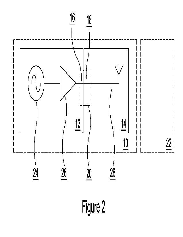
Figure 2 is a schematic diagram of the integrated applicator 10, in accordance
with
embodiments, which is referred to, for brevity, as an applicator 10. The
applicator 10 has
a microwave energy generator module 12, herein referred to, for brevity, as
simply the
CA 03184401 2022- 12- 28
WO 2022/003335
PCT/GB2021/051638
12
energy generator module and a radiating structure 14. The energy generator
module 12
has an energy output 16 for outputting generated energy. The radiating
structure 14 has
an energy input 18 for receiving energy.
It will be understood that, while the present embodiment is described with
respect to
generation and delivery of microwave energy, in other embodiments in which RF
frequency radiation is used the same principles are used.
The energy generator module 12 has microwave generating circuitry. In the
present
embodiment, the energy generator module 12 is a microwave energy generator
module
and has a signal generator or oscillator (VCO) 24 and an amplifier stage 26.
In some
embodiments, the components are such that the microwaves generated are
suitable for
application to a particular surface or, more generally, a particular target
22, for example,
tissue to be treated. The radiating structure 14 is configured to emit
electromagnetic
radiation that will be received optimally by the target 22. The radiating
structure 14 emits
radiation, for example from a radiating surface. In the present embodiment,
the radiating
structure is comprises antenna 28.
Between the energy output 16 of the energy generator module 12 and the energy,
input
18 of the radiating structure 14 there is a transmission interface 20. Energy
that is output
from the energy output 16 of the energy generator module 12 is provided to the
energy
input 18 via the transmission interface 20. The transmission interface 20 is
formed such
that it has a transmission feature having at least one of a size; dimension
and/or shape
selected to control or otherwise modify the transmission and/or reflection
properties of
the transmission interface 20. Controlling or modification of the transmission
and/or
reflection properties of the transmission interface 20 may contribute to an
optimization of
the performance of the applicator 10. For example, the power transmitted
through the
interface 20 may be maximised or transmission power losses via the interface
20 may
be minimized.
!twill be understood that a number of different transmission features may
provide desired
transmission/reflectance properties for the transmission interface 20. A
suitable
transmission feature has a shape, size or dimension that may be varied during
a design
process to allow the effect of the variation to be assessed and therefore
allowing the
design to be optimized for a specific requirement. This may allow for an
optimal operation
CA 03184401 2022- 12- 28
WO 2022/003335
PCT/GB2021/051638
13
of the applicator 10, in use. An embodiment of the applicator with a
particular
transmission feature is described with reference to Figures 3 to 6.
In use, microwave energy is generated by the energy generator module 12 and
provided
to the transmission interface 20. In accordance with the
transmission/reflectance
properties conferred on the transmission interface 20 by the transmission
feature, the
transmission interface 20 receives the energy provided to it and, permits a
first desired
portion of energy provided to it from the energy generator module 12 to be
transmitted
to the radiating structure and/or reflects a second desired portion of energy
provided to
it back to the energy generator module 12. The transmitted energy is provided
to the
radiating structure 14 to be radiated by antenna 28.
In some embodiments, the energy generator module 12 and the radiating
structure 14
may be known off-the-shelf components, for example, components that are tuned
to
have a standard impedance or other standard properties. However, it will be
understood
that, in some embodiments, at least one of these parts may be designed to be a
bespoke
component and manufactured to have particular desired properties.
In the present embodiment, the radiating structure 14 is designed such that,
when
integrated with the energy generator module 12, the radiating structure 14
presents ideal
output impedance characteristics to the energy generator module 12. Likewise,
the
radiating structure 14 is designed to possess the optimal required input
impedance
characteristics. As described in the following, the process of integrating the
two parts
may comprise selecting one or more values for design parameters of the
radiating
structure 14 and/or the energy generator module 10 to optimize one of more
properties
of the energy transferred therebetween or a related parameter. In some
embodiments,
in addition to selecting one or more design parameters of the radiating
structure 14 and
energy generator module 10, the arrangement may further also incorporate
properties
that are observed when the radiating structure 14 is presented with its ideal
or typical
target media. When the designed parts of the integrated applicator are fully
integrated
into a signal unit, they may be considered to be arranged in a balanced
configuration
and therefore the requirement for additional separate tuning elements,
matching
networks, fractions of wavelength or phase length transmission line tuning
elements is
reduced or eliminated. This may provide size and performance advantages.
CA 03184401 2022- 12- 28
WO 2022/003335
PCT/GB2021/051638
14
The design of the parts of the applicator 10 may be made in accordance with a
theoretical
framework. While different theoretical frameworks/models may be used in the
design of
the integrated applicator, a known theoretical framework includes a framework
based on
using scattering or S parameter models in which different interfaces between
different
parts of the applicator are modelled and combined using S parameter models.
Further
details regarding the theoretical framework is provided with reference to
Figures 9 to 12.
Figures 3 to 6 depicts an embodiment of the integrated applicator. Figures
3(a) and 3(b)
depict an integrated applicator, also referred to simply as the applicator
110, in
accordance with the present embodiment. Figure 3(a) shows a side view of the
applicator
110. Figure 3(a) shows the applicator 110 having an energy generator module
112 also
referred to as an energy generator module, which in the present embodiment is
a
microwave energy generator module, and a radiating structure 114. The
applicator 110
also has a transmission interface 120. Figure 3(b) shows a top view of the
energy
generator module 112 and transmission interface 120. Figure 3(b) depicts part
of the
radiating structure 114.
In further detail, in the present embodiment, the energy generator module 112
has a
printed circuit board (PCB) 130, upon which is mounted microwave power
generating
devices or circuitry 132. The energy generator module 112 is a rigid structure
and the
radiating structure 114 is a rigid structure. The energy generator module 112
is rigidly
coupled to the radiating structure 114 such that the output of the energy
generator
module 112 is provided at a transmission interface 120 and such that the input
of the
radiating structure 114 is provided at the transmission interface 120. In the
present
embodiment, the transmission interface 120 and its transmission features are
formed by
parts of the energy generator module 112 and the radiating structure 114. This
coupling
may also facilitate the transfer of thermal energy from the PCB conductive
substrate/thermal heatsink 162 into the radiating structure to provide
additional
heatsinking.
The radiating structure 114 has a coaxial input portion 134, which is a rigid
structure and
may be referred to as a coaxial input structure. The radiating structure 114
also has a
coaxial to waveguide feed section 136 and a waveguide 138. The coaxial to
waveguide
feed section 136 has a receptacle for receiving and holding the waveguide 138.
The
waveguide 138 is placed into the receptacle, which maintains electrical
continuity to the
CA 03184401 2022- 12- 28
WO 2022/003335
PCT/GB2021/051638
waveguide ground plane using a cylindrical arrangement of sprung metallic
fingers,
flared to accept the waveguide 138.
As depicted in Figures 3(a) and 3(b), in the present embodiment, the radiating
structure
5 114 is mounted to the PCB 130 and securely held in a mounted position by
two bolts
140a and 140b. Figure 3(a) shows first bolt 140a and Figure 3(b) shows both
first bolt
140a and second bolt 140b. Corresponding pairs of recesses are provided in the
PCB
130 and coaxial input portion 134 of the radiating structure 114. For each of
the pair of
bolts, a first recess is provided in PCB 130 and a second recess is provided
in the PCB
10 130. The recesses are provided, such that for each bolt, a pair of
aligned recesses are
presented for the bolt to pass through thereby mechanically securing the
energy
generator module 112 and radiating structure 114 together. It will be
understood that
other securing mechanisms may be used in other embodiments to secure the
radiating
structure 114 and energy generator module 112 together.
Figure 3(b) shows a top view of the applicator 110, with the coaxial input
portion 134 of
the radiating structure 114 shown. Also shown in Figure 3(h) is a microstrip
element 142
of the energy generator module 112 which provides an output for generated
microwave
energy from the module. The microstrip element 142 is printed on the upper
surface of
the printed circuit board 130. Figure 3(b) also shows bolts 140a and 140b.
In the present embodiment, the energy output of the energy generator 112
comprises a
microstrip structure of which the microstrip element 142 forms a part. In the
present
embodiment, the energy input of the radiating structure 114 comprises the
coaxial input
portion 134 and its respective elements. The transmission interface 120, its
transmission
features and the energy input and outputs provided at the transmission
interface 120 are
described in further detail in the following, for the present embodiment.
As can be seen from Figures 3(a) and 3(b) and as descried in further detail
with reference
to Figures 4 and 5, the radiating structure 114, in particular the coaxial
input portion 134,
and the energy generator module 112, in particular, the microstrip element 142
together
form a transmission feature at the transmission interface 120. In the present
embodiment, the transmission feature 120 is a step feature characterised by an
overlap
length 144. It will be understood that, while in the present embodiment, the
transmission
feature 120 is a step feature, alternative transmission features may be
implemented at
the transmission interface 120. Alternative transmission features may include
tapered or
CA 03184401 2022- 12- 28
WO 2022/003335
PCT/GB2021/051638
16
gradual transition features. In further detail, in the present embodiment, the
step feature
provides an overlap between the radiating structure 114, in particular the
coaxial input
portion 134 that provides an energy input to the radiating structure 114 and
the energy
generator module 112, in particular the microstrip element 142, which forms
part of an
energy output for the energy generator module 112.
As described in detail with reference to Figures 7 and 8, the overlap length
144
characterising the step feature may have different values in different
embodiments.
Variation of the overlap length 144 may control the reflection and
transmission
characteristics of the transmission interface 120. In the present embodiment,
the overlap
length is 3mm, however, this could be in a range between 1mm to 8mm, or for
example
3 mm to 6mm. The overlap length is in a direction substantial parallel to the
propagation
of the energy generated by the energy generator module 112. The overlap length
is
parallel to a longitudinal axis of the radiating structure 114 and the energy
generator
module 112.
Due to the presence of the transmission interface 120, no flexible extendable
transmission line, for example, no variable length co-axial cabling is
required between
the energy generator module 112 and the radiating structure 114.
In the present embodiment ground plane continuity is provided by including top
ground
plane connections to the radiating surface or antenna of the radiating
structure 114. The
conductive bolts 140a, 140b may also mate with an exposed ground plane on the
underside of the PCB 130 for an additional ground plane connection.
Figure 4 is a cross-sectional illustration of the transmission interface 120.
Figure 4 shows
parts of the coaxial input portion 134. The coxial input portion 134 has an
inner conductor
150 coaxial with an outer conductor 152. At the input end of the coaxial input
portion 134
(the end provided proximal to the coupled energy generator module 112) a
coaxial
dielectric material 154 substantially fills the space between the inner
conductor 150 and
the outer conductor 152. The coaxial dielectric material 154 may also be
referred to as
an insulating material. The coaxial dielectric material 154 holds the inner
conductor 150
and outer conductor 152 in place and electrically isolates the inner conductor
150 from
the the outer conductor 152.
CA 03184401 2022- 12- 28
WO 2022/003335
PCT/GB2021/051638
17
Figure 4 shows the microstrip structure 156 of the energy generator module 112
in further
detail. The microstrip structure 156 has a layered structure comprising of an
upper
conductor layer corresponding to the microstrip element 142, provided on a
dielectric
layer 158 and a ground plane layer 160. These layers are provided on a
conductive
substrate/thermal heatsink 162.
Figure 4 shows a cross-sectional view of the step feature between the
microstrip
structure 156 and the coaxial input portion 134. In Figure 4, cross-shaded
elements are
conductive metals and dot shaded elements are dielectric insulators. As can be
seen
from Figure 4, the step feature is created by removing a portion of the
coaxial input
portion 134, in particular, the inner conductor 150, the outer conductor 152,
the coaxial
dielectric material 154 to create a void in the coaxial input portion 134, the
void having
an upper surface in the inner conductor 150 and a side surface of inner
conductor 150,
coaxial dielectric material 154 and outer conductor 152. The coaxial input
portion 134
and microstrip structure 156 are then arranged such that the distal portion of
the
microstrip structure 156 is placed into the void. When in place, at least part
of the upper
surface of the microstrip structure 156 abuts an upper surface of the void and
the side
surface of the microstrip structure 156 abuts the side surface of the void
such that the
microstrip structure 156 is fitted into the void of the coaxial input portion
134. When
arranged in postion, at least part of the microstrip element 142 of the
microstrip structure
156 is in direct contact with the inner conductor 150 along a length
corresponding to the
overlap length 144.
In the present embodiment, as can be seen from Figure 4, as described above, a
first
surface of the coaxial input portion 134 is in direct contact with a first
surface of the
microstrip structure 156 and a second surface of the coaxial input portion 134
is in direct
contact with a second surface of the microstrip strcuture 156, wherein the
second
surfaces are perpindicular to the first surfaces. It will be understood that,
in some
embodiments, the first and/or second surfaces are not provided in direct
contact but
rather provided at a separation equal to a pre-defined coupling distance, for
example,
1mm.
Figure 5 depicts a further, perspective view of the transmission interface
120, in particular
Figure 5 shows the step feature described with reference to Figures 3 and 4.
As can be
seen from Figure 5, the step feature comprises both an overlap width 164
corresponding
CA 03184401 2022- 12- 28
WO 2022/003335
PCT/GB2021/051638
18
to the radius of the proximal end of the coaxial input portion 134 and the
overlap length
144. The step feature also has a height. The dielectric layer 158 of the
microstrip
structure 156 is exposed at the upper surface so that the upper surface of the
printed
circuit board has both a conductive portion and an insulating portion. The
coaxial input
portion 134 has a width such that the dielectric material 154 of the coaxial
input portion
134 is in contact with part of the exposed dielectric layer 158 of the
microstrip structure
156. The step feature thus comprises a dielectric or insulting surrounding for
the
conductive microstrip element 142 formed by dielectric material 154 of the
coaxial input
portion 134 and dielectric layer 158. The surround substantially surrounds the
conductive
microstrip element 142 of the microstrip structure 156 thereby acting as an
insulator. It
is also noted, from Figure 5, that there is no insulating dielectric layer
between the
contacts i.e. a direct conductive connection is made.
The above step feature is just one example of a transmssion feature that can
be provided
at the transmission interface 120. The step feature is an example of a coaxial
step
discontinuity used to interface with a microstrip trace on a PCB. The
microstrip trace is
intended to be as short as possible and functions as a connection to the
antenna and is
not intended to be tunable transmission line.
Figure 6 is a photographic representation of the integrated applicator 110.
Figure 6
depicts a number of elements of the integrated applicator 110 described with
reference
to Figures 3, 4 and 5.
In the present embodiment, the radiating structure 114 is mounted directly
onto the
energy generator module 112 and is secured from beneath using bolts 140a, 140b
as
depicted in Figures 3(a) and 3(b). It will be understood that the electrical
connections of
the device can include, for example, direct contact, solder, conductive epoxy
or
PariPosere anisotropic elastomer material. Once secured in position it will be
understood that in the present embodiment, the radiating structure 114 and
energy
generator module 112 are fixed relative to each other, and are not moveable
i.e. do not
slide. The integrated device 110 offers the advantage that there is no
requirement for
moveable or tuneable elements, as all optimisation is achieved during the
design stage,
in which values for one or more design parameters are selected.
CA 03184401 2022- 12- 28
WO 2022/003335
PCT/GB2021/051638
19
In the above-described embodiments, a step feature is described as a non-
limiting
example of a transmission feature at the transmission interface. However, it
will be
understood that the transmission feature(s) may comprise any form of
discontinuity at
the transmission interface between the energy output and the energy input. As
a further
non-limiting example, a width of the energy input of the radiating structure
and/or the
energy output of the energy generator module may be selected such that there
is a
mismatch in widths thereby providing an interruption or discontinuity between
the energy
output and energy input. Similar mismatches in other dimensions may be
designed, for
example, the height of the energy input and output. Mismatches in shapes can
also be
implemented, for example, a tapered structure may be selected. The
transmission
feature may comprise a mismatch between the energy output and energy input,
for
example, in size, shape or other dimensions, or other discontinuity, thereby
to introduce
a transmission inefficiency at the transmission interface.
As a further example, the at least one transmission feature may alternatively
or
additionally include other features that provide discontinuities at the
transmission
interface, for example, a slot or a gap or a protrusion in at least one of the
energy output
of the energy.
With reference to the above-described embodiment in which a coaxial structure
is
coupled to a microstrip structure, a discontinuity may be provided in the
microstrip or the
coaxial structure, or both. For the microstrip, any region that was too thin
or too wide
could cause a discontinuity. In terms of the coaxial structure, in the above-
described
embodiment a discontinuity was introduced in the inner conductor. However, it
will be
understood that the transmission feature may comprise at least one of the
following non-
limiting examples: a change in a coaxial ratio (the ratio between the inner
conductor and
outer conductor radius), a longitudinal slot in the coaxial outer conductor, a
radial slot
gap in the coaxial outer conductor or a perturbation or protrusion in the
outer conductor.
A conductive pin or washer could provide a protrusion in the outer conductor.
As described in the following, components of the intergrated applicator are
optimized
during a design process. The overlap feature is one of a number of antenna
design
factors that may be be used to adjust performance during design.
CA 03184401 2022- 12- 28
WO 2022/003335
PCT/GB2021/051638
Figures 7(a) and 7(b) are plots (200a, 200b) depicting simulated values for S
matrix
parameters. In particular, Figures 7(a) and 7(b) illustrate the variation of
the S matrix
parameters Si1 and S21 as a function of radiation frequency. Sii represents
the amount
of power reflected from the cascaded radiating structure and may be referred
to as the
5 reflection coefficient. If this parameter is zero, then all power is
reflected from the
radiating structure and nothing is radiating. S21 represents the transmission
loss and
conversely the lower this loss the higher the energy transferred. The Y-axis
202 for both
plots of Figures 7(a) and 7(b) is a log-scale and have units of dB. The X-axis
204 for
both plots is frequency.
In the present embodiment, the parameters Sii and Si2 take into account
target/tissue
properties. In particular, parameter Sii in relation to Figures 7(a) and 7(b)
relate to a
cascade of antenna and target/tissue properties (i.e. references 50 and 52 of
Figure 11).
In other embodiments in which a full cascaded model is implemented, the
parameters
also take into account the properties of the amplifier and source models
(references 54
and 56 of Figure 11).
A first plotted line 206 in Figure 7(a) is representative of S11 as function
of frequency. A
second plotted line 208 in Figure 7(b) is representative of S21 as a function
of frequency.
For parameter S11, it will be understood that, in some embodiments, anything
that has
values below -10dB may be considered as acceptable. For parameter S21, it will
be
understood that, in some embodiments, a transmission loss close to zero may be
desirable. In other embodiments, a proportion of reflected energy may be
desirable.
During the design process, values for design parameters of the coupling
interface are
selected and varied to simulate the effect of variation of the parameter
values on the S-
matrix parameters. In Figure 7(b), values for S-parameters are plotted to
illustrate the
effect of variation of the overlap length (illustrated as numeral 144 in, for
example, Figure
4). The overlap length relates to the size of overlap between the co-axial
input portion
134 and the nnicrostrip structure 156. It will be understood that the overlap
length may or
may not be varied directly; it may also be varied through one or more other
parameters
on which the overlap length is dependent. In this embodiment, the overlap
length is
dependent on the coaxial distance parameter (coax_d). For each value of the
parameter
being varied, in this case, the coaxial distance (coax_d) there is a pair of
plotted lines
CA 03184401 2022- 12- 28
WO 2022/003335
PCT/GB2021/051638
21
corresponding to the values for S11 and S21. Figure 7(b) shows pairs of
plotted lines for
values for the coaxial distance for 5mm, 6mm and 7mm (corresponding to overlap
lengths of 3mm, 2mm and 1mm, respectively).
For the S11 parameter, plotted lines 210a, 212a and 214a correspond selection
of the
value for the coaxial distance parameter to be 5mm, 6mm and 7mm, respectively.
For
the S21 parameter, plotted lines 210b, 212b and 214b correspond to selection
of the value
for the coaxial parameter to be 5mm, 6mm and 7mm, respectively.
Figures 8(a), 8(b) and 8(c) are screenshots of a graphical interface 300 used
for
designing the applicator. On the left side of Figures 8(a), 8(b) and 8(c) is a
user interface
panel 302 that allows a user to select different values for design parameters.
These
parameters include:
microstrip_L (microstrip conductive element, or tab, length)
Substrate_W (substrate width)
Substrate_H (substrate height)
Gnd_H (ground layer thickness)
Trace_W (microstrip conductive element width)
Trace_H (microstrip conductive element thickness)
Waveport_W (port width)
Waveport_H (port height)
Coax_d (coax/microstrip relative position)
Diel (coaxial dielectric radius)
Oc (outer conductor radius)
Coax_I (coax length beyond the overlap)
I crad. (inner conductor radius)
The wave port height and width are only relevant to the modelling software and
are not
physical features. These were arbitrarily chosen (approximately 2 times the
substrate
height and approximately 2/3 of the substrate width).
On the right hand side of Figures 8(a), 8(b) and 8(c) is a viewing panel 304
for viewing a
graphical representation of the applicator. Figure 8(a) shows an overhead (top
down)
CA 03184401 2022- 12- 28
WO 2022/003335
PCT/GB2021/051638
22
graphical representation of a view of a first simulated transmission interface
between the
coaxial input structure 134 and the microstrip structure 156.
Figures 8(b) and 8(c) show side views of a second and third simulated
transmission
interface, respectively, between the coaxial input portion 134 and the
microstrip structure
156. Different values for the overlap length have been selected. In Figure
8(a), the first
simulated transmission interface has an overlap length of Omm (corresponding
to a
coaxial distance parameter of 8mm). In Figure 8(b), a second simulated
transmission
interface is depicted having an overlap length 144b of 2mm (coaxial distance
of 6 mm).
In Figure 8(c) a third simulated transmission interface is depicted that has
an overlap
length 144c of 3mm (corresponding to a coaxial distance of 5mm).
In these embodiments, only a single design parameter is varied, however, it
will be
understood that in other embodiments, more than one design parameter may be
varied
and/or selected.
The coaxial distance is related to the overlap length (the size of the step
feature). In
particular, in the present embodiment, the microstrip element 142 is retained
at a fixed
length (8mm) and the parameter of coaxial distance (the distance between a
first end of
this fixed length and the distal end of the microstrip structure 156). It will
be understood
that selection of this parameter determines the size of the overlap length. In
particular,
in Figure 8(a), the value of this parameter is 8mm which is equal to the
microstrip length
parameter (microstrip_L) and therefore there is no overlap (overlap length is
Omm). In
Figure 8(b), the value of this parameter is set to 6mm which is 2mm less than
the
microstrip length parameter of 8mm (microstrip_L) and therefore there is an
overlap
(overlap length is 2mm). In Figure 8(c), the value of this parameter is set to
5mm which
is 3mm less than the microstrip length parameter of 8mm (microstrip_L) and
therefore
there is an overlap (overlap length is 3mm).
In Figures 8(a), 8(b) and 8(c) a radiating boundary is modelled as a boundary
box 802.
The software assumes all other regions are perfect conductors (metal) so the
model
describes a coax inside a block of metal that has the variable step introduced
to fit onto
a PCB. Boundary box 802 is an approximation of radiation into free-space and
is not a
physical 3D feature of the model but rather provided as part of the modelling
process.
CA 03184401 2022- 12- 28
WO 2022/003335
PCT/GB2021/051638
23
In addition to the design of the transmission interface, further design
parameters of the
radiating structure and/or energy generator module or components thereof may
be
selected to control performance of the applicator. In known applicators, an
antenna may
be designed to impedance match to a 50 ohm transmission line and the energy
generator
module may be designed to impedance match to a 50 ohm transmission line. In
such
applicators, matching networks and other tuning elements are provided to
compensate
for mismatches between the components. In the present embodiments, the
components
are designed with reference to an underlying model i.e. taking into account
the operation
of the other components and the application target, such that when the
components are
plugged together the devices operate optimally.
For such a method, it has been found that there may be advantages in an
integrated
applicator that uses a radiating structure or a part thereof, for example, an
antenna that
is designed to have an input or other part that causes the antenna to reject
energy. Such
an antenna may be considered to provide what may be classed as sub-optimal
performance when considered in other systems. In the integrated applicator,
the amplifier
of the generator module receives feedback from the antenna representative of
the
rejected energy and, in response to this feedback, causes further energy to be
transmitted to the antenna.
It will be understood that the step discontinuity in the present embodiment
does not alter
the overall electrical length (path phase) and operates at 8GHz within
dimensions less
than 1/4 of a wavelength for a guided wave in the microstrip. For the
following model
parameters: dielectric constant of the printed circuit board (Er) of 4.4, a
microstrip trace
width (W) of 4mm and a board height (H) of 2mm (thickness), the calculated 1/4
wavelength in the board is 5.125mm. It will be understood that the dielectric
compresses
the electromagnetic wavelength compared to the equivalent free space
wavelength.
These dimensions are within one tenth of a wavelength and cannot be considered
to
constitute tuning as the discontinuity within this region creates a deliberate
mismatch
and adjustable level of loss that can be utilised.
The design of the parts of the applicator may be made in accordance with a
theoretical
framework. Further comments on the theoretical framework are provided in the
following.
CA 03184401 2022- 12- 28
WO 2022/003335
PCT/GB2021/051638
24
As discussed above, the design is such that additional matching networks may
be
avoided. Matching networks are often used for modelling applicators. An
example of a
two-port matching network arrangement is illustrated in Figure 9. In this
standard theory,
a device with full 2-port S-parameters can be matched both to a generator
(ZsouRcE) and
to a load (ZLoAD) by means of Input (Fs/FIN) and output (FL/Foul) matching
networks. In
this theory, the output section 400 could represent an antenna with a tissue
dielectric
acting as the load. In this description, Z is impedance and F is a reflection
coefficient.
Underpinning the present embodiments, is a concept similar to the concept of a
conjugate match, the condition for maximum power delivery to a load, in which
the
impedance seen looking to the load at a point in a transmission line is the
complex
conjugate of that seen looking to the source. A conjugate match states that a
maximum
power is transferred between a source (like a transmitter) and a load (like an
antenna),
when the source impedance is the complex conjugate of the load impedance. The
design
principle followed is different to a single-end conjugate match and in
principle follows
Everitt's conjugate match theorem for lossless networks which states that if a
conjugate
match exists at any port in the cascade, then a conjugate match exists at
every port in
the cascade, including the input and output ports connected to the source and
load with
all available power is delivered to the load.
However, in reality transmission networks are not lossless, and although in
theory a
system-wide conjugate match in a network comprising lossy elements might be
mathematically possible in practical terms the best solution is maximum power
transfer
which traditionally requires consideration of matching in both directions to
ensure optimal
power transfer. By minimising losses in the matching networks and by
considering the
quality factor, Q of load and source elements the closest approximation to a
near system-
wide conjugate match may be achieved.
As described above, in accordance with embodiments, no separate external
matching
networks or tuneable transmission lines are required for the integrated
applicator. The
radiating structure (or antenna element) is designed to bilaterally satisfy
the matching
requirement in addition to the radiating requirement by providing a very low-
loss
matching network function in each direction between the final target and the
energy
generator module or power source. In the present embodiment, the transmission
line
path from the energy source to the treatment applicator may be eliminated
thereby
CA 03184401 2022- 12- 28
WO 2022/003335
PCT/GB2021/051638
reducing losses that would occur in the system via this transmission line and
the
additional energy required. This may lead to an improvement in efficiency.
In instances where the energy generator module or power source has an un-
matched
5 RF/Microwave transistor which has its own particular scattering
parameters the same
optimisation can be achieved by judiciously utilising a specific antenna-to-
target
mismatch in combination with antenna phase properties to present the desired
complex
reactive impedance as required the RF/Microwave transistor. In this way both
elements
can be co-designed as a single integrated energy transmission network.
Figure 10 shows a schematic diagram illustrating the theoretical framework
underpinning
a design process of the integrated applicator, in accordance with embodiments.
Figure
10 illustrates the different interfaces that may be considered when designing
the
applicator 10. In this framework, scattering matrices for different interfaces
of the
applicator are described.
Figure 10 shows a representation of the integrated applicator 10. Figure 10
depicts a
combined antenna and tissue S-parameter model 30. The antenna and tissue S-
parameter model 30 has an antenna element 32 (provided as part of the
radiating
structure) and certain properties of the antenna element 32 are represented in
Figure
10, including match 34, phase 36 and resonant bandwidth (Quality-factor) 38.
In Figure 10, a generator-antenna interface model 40 is represented. In Figure
10, the
output matching networks (FL/FouT) from theory are represented by the designed
interaction 42 between the antenna and tissue 22 in combination with the
interaction
between generator and antenna 40.
Calculation and/or determination of design parameters may be implemented using
a
cascaded design approach. In this illustration, each S-parameter model is
cascaded or
otherwise combined to form an overall model of the integrated applicator.
In this example, the dielectric properties of the tissue target (which are
either
measured/sampled or simulated) are represented by 50. The tissue model is
cascaded
with a baseline S-parameter model for the antenna 52. In some embodiments, the
combined network of tissue model 50 and antenna model 52 can then be optimised
to
CA 03184401 2022- 12- 28
WO 2022/003335
PCT/GB2021/051638
26
present the desired impedance to the preceding stages: amplifier stage 54 and
generator
source stage 56 thereby to deliver the optimum energy to the tissue by
adapting
combined antenna/tissue attributes of match 34, phase 36 and resonant
bandwidth
(Quality-factor) 38 in the antenna model.
The S-parameter models may represent simple numerical cascaded S-matrix models
or
may also be hierarchically formed using or including hybrid combinations of S-
parameter
models and simulation S-parameter outputs of full-wave 3D solvers e.g. HFSS,
XFdtd,
COMSOL Multiphysics, FEKO etc. These 3D solvers can include complex
electromagnetic interactions between each stage therefore one or more stages
may be
included in a 3D model that may be cascaded with an S-matrix model in the same
or in
another circuit-level simulator e.g. Microwave Office, Sonnet, ADS etc. S-
matrix models,
Y-matrix models or Z-matrix models or any combination therefore may be used
depending upon the simulator used.
In addition, cross coupling of energy 58 from the antenna stage 52 to the
amplifier stage
54, may also be employed to optimise the design further. This energy may be
coupled
directly e.g. cavity mode cross-coupling or indirectly by parasitic coupling.
This method
provides further options to employ finite transmission zeros which can be
utilised to
improve bandwidth or feedback to increase amplifier efficiency. This technique
can also
be achieved by loading the input of the antenna with a second-order extracted-
pole unit
(EPU) composed of a pair of mutual coupled resonators negating the need for
physical
cross-coupling. This can be realised by utilising stepped cross-sections or
tab-cross
feeds in the case of waveguide fed antennas.
In this regard, the overall design can also be treated in terms of coupling
matrices. Figure
12 represents coupling matrices, may employ coupling matrix synthesis methods
to
achieve the desired overall performance.
By implementing this invention, the design can be made more efficient, more
compact
and can eliminate the requirement for tuneable transmission lines, tuning
stubs or other
similarly physically distributed (or electronically or mechanically actuated)
tuning
arrangements that would have been necessary to improve efficiency.
CA 03184401 2022- 12- 28
WO 2022/003335
PCT/GB2021/051638
27
In terms of fabrication, the integrated generator/antenna may be constructed
from
lightweight materials to permit a reduction in the mass. In some embodiments,
the
applicator may also take advantage of the integrated construction to dissipate
excess
heat into metallic or thermally conductive elements within the antenna to
reduce size
further. The integrated generator/antenna may also have particular thermal
interface
points that could mate with heatsinking elements e.g. Cu-Cu brackets or
pyrolytic carbon
or thermally annealed pyrolytic graphite (APG) materials or combinations
thereof e.g.
Cu-APG or Aluminium-APG interface plates.
Thermal interface points may be provided for example, at the transmission
interface 120
region and via the bolt 140a and 140b, depicted in Figures 3(a) and 3(b). The
entire PCB
130 depicted in Figures 3(a) and 3(b) is provided on a metal carrier/substrate
that sinks
heat from the microwave power devices provided in the PCB 130. The additional
bulk
metal work of the radiating structure 114 may also sink some of this heat.
Embedded
"copper coin" methods may be implemented, between the microwave power device
and
base of PCB 130 to get heat into the substrate from the PCB 130.
It will be understood that a power source is provided for the microwave power
generator
module to generate microwave power. The power source may be from a port or
electrical
power loom intended to power or communicate to peripherals or tools. Suitable
power
schemes are known in the art and are not discussed in further detail.
In further embodiments, the device may have a controller for controlling one
or more
operational parameters of the device. For example, system/applicator
temperatures,
forward and reflected power, duty cycle, antenna performance attributes or
other relevant
parameters may be controlled. A feedback mechanism may also be provided to
control
operational parameters based on feedback from the device. It may also access
communications or networks to communicate with an external controller to
provide
feedback.
A skilled person will appreciate that variations of the enclosed arrangement
are possible
without departing from the invention. Accordingly, the above description of
the specific
embodiment is made by way of example only and not for the purposes of
limitations. It
will be clear to the skilled person that minor modifications may be made
without
significant changes to the operation described.
CA 03184401 2022- 12- 28