Note : Les descriptions sont présentées dans la langue officielle dans laquelle elles ont été soumises.
CA 03187364 2022-12-15
WO 2021/253122
PCT/CA2021/050821
SYNCHRONOUS RECTIFICATION TO IMPROVE EFFICIENCY OF
ELECTRICITY CONVERSION FOR HARVESTING ENERGY FROM LOW
VOLTAGE SOURCES
FIELD
[0001] Aspects of this disclosure relate to methods and systems for
converting
energy harvested from low voltage sources.
BACKGROUND
[0002] Many sources of energy that can be harvested are in the form of
electricity
or can be readily converted to it. However, in many practical situations,
these
electricity sources are either weak, with too high or too low a voltage, or
have other
issues. Consequently, these sources are rarely directly useful to low power
electronic
devices, for example in wireless sensor networks and Internet of Things (IoT)
applications, where a relatively steady supply of a direct current (DC)
voltage of a
few volts may be required.
[0003] It would be advantageous to have systems and methods for
efficiently and
robustly converting low voltage DC electricity, such as from a thermo-electric
generator (TEG), for example a thermopile, into a usable form, for example for
use
by wireless sensor networks and IoT applications.
[0004] Some systems employ a step-up DC-DC converter to turns low
voltage DC
electricity from a TEG into a usable form by converting a low voltage DC input
to a
higher voltage DC output. There are various step-up DC-DC converters for TEG
energy harvesting available on the market, and many of these schemes rely on
an
oscillator to perform' the conversion. Examples include those proposed in the
following three references:
[0005] (a) EnOcean GmbH, ECT 310 Perpetuum,
http s ://www. enocean. com/en/enocean modules/ect-310-perpetuum/.
[0006] (b) Linear Technology Corporation, LTC3108 - Ultralow Voltage
Step-
Up Converter and Power Manager, http://www.linear.com/product/LTC3108.
1
CA 03187364 2022-12-15
WO 2021/253122
PCT/CA2021/050821
[0007] (c)
Dario Grgie, Tolgay Ungan, Milo S Kostie, and Leonhard M. Reindl,
"Ultra-Low Input Voltage DC-DC Converter for Micro Energy Harvesting,"
PowerMEMS 2009, pp. 265268, Washington DC, USA, December 1-4, 2009.
[0008] Each of
the three schemes introduced above work in a certain input range
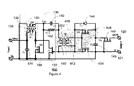
and at a relatively low efficiency. Their turn-on source conditions and
efficiencies are
summarized in Table 1 below, where VOC is the open-circuit voltage of the TEG
device and RTEG is the internal resistance (also known as the source
resistance) of
the device. The turn-on source conditions for this example include turn-on
voltage
and RTEG. The turn-on voltage is the minimum voltage required from the source
before the DC-DC converter starts to produce a DC output voltage with an
absolute
value greater than that of the input.
[0009] Table 1
shows the turn-on source conditions and efficiencies of existing
schemes:
TABLE 1
Turn-on source conditions and efficiencies of existing schemes
ECT310 by LTC3108 by Linear Dail GrgiC
EnOcean Technology et al.
Turn-on VOC = 20 mV & VOC = 50 nil/ & VOC = 10 inV &
source RTEG = 2 .c2 RTEG = 20 S2 RTEG = 50 Er-2'
condiLion or
VOC =5() mV & VOC = 100 mV &
RTEG = 50 .c2 RTEG = 50 -2
Elliciency 30% 20-40% <18%
Note that, for above-noted scheme (c) described by Dario Grgie etal., VOC at
RTEG
= 50 S2 is derived from information provided in the abstract of the third
reference: Vcc
= 6 mV (closed-circuit input voltage) and input power of 490 nW.
[0010] Figure 1
shows prior art step-up DC-DC converter 110, as described in
the applicant's co-pending application United States Application No.
16/131,650, the
entire contents of which are incorporated herein by reference. Step-up DC-DC
converter 110 comprises a lower turn-on voltage and has been shown to possess
an
efficiency of at least 45%. While this efficiency is impressive, even higher
efficiencies
in energy harvesting are desirable. In a typical application, low-voltage DC
electricity
2
CA 03187364 2022-12-15
WO 2021/253122
PCT/CA2021/050821
is converted from a thermo-electric generator (TEG) into another DC potential
of a
few volts to drive low-power electronic devices such as those in wireless
sensor
networks and Internet of Things (IoT). Accordingly, any improvement in
efficiency
enables a step-up DC-DC converter to better utilize the very limited energy
available
and provide more power to the load.
[0011] Several
approaches have been proposed to further boost to the efficiency
of the above-noted prior art step-up DC-DC converter 110. For example, some
approaches employ synchronous rectification, such as, the LM5122 Wide-Input
Synchronous Boost Controller, manufactured by Texas Instruments, U.S.A. and
the
UCC24630 synchronous rectifier controller, manufactured by Texas Instruments,
U.S.A., in an attempt to precisely control the timing for the switches.
Unfortunately,
such sophisticated controllers consume significant overhead power, which is
undesirable in TEG energy harvesting applications. There also exist "self-
driven"
synchronous rectification schemes which do not need an explicit controller,
and hence
save the overhead power, however, these schemes are driven by the voltages
applied
to the MOSFET switches, and cannot guarantee an appropriate timing, which is
essential for assuring a high efficiency.
[0012] Given
the difficulties discussed above, especially the need to dedicate any
overhead power on switch control, synchronous rectification has not been
adopted
extensively in the realm of DC-DC step-up conversion for energy harvesting.
SUMMARY
[0013] In one
aspect of the disclosure, there is provided a DC-DC converter for
converting a low voltage DC input to a higher voltage DC output, the DC-DC
converter comprising:
an oscillator comprising a first relatively voltage sensitive and
relatively low power transistor and a second relatively voltage insensitive
and
relatively high power transistor, the oscillator producing an AC signal from
the low
voltage DC input;
a first transformer for converting the AC signal produced by the
oscillator to a higher voltage AC signal;
3
CA 03187364 2022-12-15
WO 2021/253122
PCT/CA2021/050821
an autonomous, synchronous voltage-doubling rectification circuit for
converting the higher voltage AC signal to the higher voltage DC output, the
autonomous, synchronous voltage-doubling rectification circuit comprising a
second
transformer, a first shunt switch and a second shunt switch; and
wherein current through the second transformer controls the
synchronous rectification.
[0014] In one
aspect of the disclosure, there is provided a DC-DC converter for
converting a low voltage DC input to a higher voltage DC output, the DC-DC
converter comprising:
an oscillator comprising a first relatively voltage sensitive and
relatively low power transistor and a second relatively voltage insensitive
and
relatively high-power transistor, the oscillator producing an AC signal from
the low
voltage DC input;
a first transformer for converting the AC signal produced by the
oscillator to a higher voltage AC signal;
an autonomous, synchronous voltage-doubling rectification circuit for
converting the higher voltage AC signal to the higher voltage DC output,
wherein
the autonomous, synchronous voltage-doubling rectification circuit comprises a
second transformer, a first shunt switch and a second shunt switch; and
wherein the first and second transistors of the oscillator are such that
the oscillator is initially turned on when the low voltage DC input is
sufficiently
high to start the oscillator initially using only the first relatively high-
sensitivity low
power transistor, and the second transistor turns on when the voltage on a
secondary
side of the transformer exceeds the turn-on voltage of the second transistor.
[0015] In
another aspect of the disclosure, there is provided a method of
converting a low voltage DC input to a higher voltage DC output, the method
comprising:
producing an AC signal from the low voltage DC input using an
oscillator comprising a first relatively voltage sensitive and relatively low
power
transistor and a second relatively voltage insensitive and relatively high
power
transistor, by starting up oscillation of the oscillator when the low voltage
DC input
4
CA 03187364 2022-12-15
WO 2021/253122
PCT/CA2021/050821
is sufficiently high to start the oscillator initially using only the first
relatively high-
sensitivity low power transistor, and turning on the second transistor when
the
voltage on a secondary side of the transformer exceeds the turn-on voltage of
the
second transistor;
converting the AC signal produced by the oscillator to a higher
voltage AC signal with a first transformer;
rectifying the higher voltage AC signal to produce the higher voltage
DC output using at least a second transformer, a first shunt switch and a
second
shunt switch forming a rectifier; and using an input current to the rectifier
to control
the timing of the first shunt switch and the second shunt switch to maximize
efficiency.
[0016] In another aspect of the disclosure, there is provided an
autonomous,
synchronous voltage-doubling rectification circuit for converting the higher
voltage
AC signal to the higher voltage DC output, the synchronous rectification
circuit
comprising:
a transformer comprising:
a first shunt switch coupled to the transformer;
a second shunt switch coupled to the transformer; and
wherein the synchronous rectification is controlled solely by current through
the transformer.
[0017] In another aspect of the disclosure, there is provided a DC-DC
converter
with full synchronous rectification scheme that consumes minimal overhead
power and
comprises switches that are controlled by the current, as opposed to voltage,
through the
transformer, which results in a robust and simple synchronous rectifier whose
timing is
appropriate and optimized for maximizing the efficiency, especially in
harvesting TEG
energy applications.
BRIEF DESCRIPTION OF THE DRAWINGS
[0018] Several exemplary embodiments of the present disclosure will
now be
described, by way of example only, with reference to the appended drawings in
which:
[0019] Figure 1 shows a schematic of a prior art step-up DC-DC
converter;
CA 03187364 2022-12-15
WO 2021/253122
PCT/CA2021/050821
[0020] Figure 2 shows a rectification portion extracted from the prior
art step-up
DC-DC converter of Figure 1;
[0021] Figure 3 shows a simplified schematic of a synchronous (active)
rectification circuit of the prior art step-up DC-DC converter of Figure 1;
[0022] Figure 4 shows a DC-DC step-up converter featuring synchronous
rectification with synchronous rectification control transformer TF2;
[0023] Figure 5 shows a DC-DC step-up converter featuring synchronous
rectification with synchronous rectification control transformer TF2 split
into two
transformers with a series primary connection, in one implementation;
[0024] Figure 6 shows a DC-DC step-up converter featuring synchronous
rectification with synchronous rectification control transformer TF2 split
into two
transformers with a parallel primary connection, in one implementation;
[0025] Figure 7 shows a flowchart outlining exemplary steps for a
method of
converting a low voltage DC input to a higher voltage DC output, in one
exemplary
implementation; and
[0026] Figure 8 shows a graph with a comparison of preliminarily
measured
efficiency values.
DETAILED DESCRIPTION
[0027] The following detailed description refers to the accompanying
drawings.
Wherever possible, the same reference numbers are used in the drawings and the
following description to refer to the same or similar elements. While
embodiments of
the disclosure may be described, modifications, adaptations, and other
implementations are possible. For example, substitutions, additions, or
modifications
may be made to the elements illustrated in the drawings, and the methods
described
herein may be modified by substituting, reordering, or adding stages to the
disclosed
methods. Accordingly, the following detailed description does not limit the
disclosure.
Instead, the proper scope of the disclosure is defined by the appended claims.
[0028] Moreover, it should be appreciated that the particular
implementations
shown and described herein are illustrative of the invention and are not
intended to
otherwise limit the scope of the present invention in any way. Indeed, for the
sake of
brevity, certain sub-components of the individual operating components, and
other
6
CA 03187364 2022-12-15
WO 2021/253122
PCT/CA2021/050821
functional aspects of the systems may not be described in detail herein.
Furthermore,
the connecting lines shown in the various figures contained herein are
intended to
represent exemplary functional relationships and/or physical couplings between
the
various elements. It should be noted that many alternative or additional
functional
relationships or physical connections may be present in a practical system.
[0029]
Referring to Figure 1, there is shown a circuit diagram of a power supply
and load provided by a step-up converter circuit, generally designated by
numeral 100,
and as described in the applicant's co-pending application United States
Application
No. 16/131,650, the entire contents of which are incorporated herein by
reference.
Low voltage source 100 is connected via positive and negative input terminals
106,107 to the provided step-up converter circuit which is generally indicated
at 110,
which in turn is connected via positive and negative output terminals 120,121
to load
122. Low voltage source 100 and DC-DC converter 110 together form the power
supply that powers the load 122. Low voltage source 100 is modelled as a
voltage
source 102 that produces an input voltage VTEG on input terminal 106 relative
to Vo
on input terminal 107, and an input resistance RTEG 104.
[0030] The
schematic of step-up DC-DC converter 110 will be described in detail
followed by a description of its functionality. Capacitor Ci 135 is connected
across
the input terminals 106, 107 to reduce the impact of the fluctuating load
current and
to suppress potential interference. There is shown transformer 130 having
primary
winding 134 and secondary winding 132, with the polarity configuration of the
transformer windings being indicated by the phasing dots. Primary winding 134
has a
predetermined number of turns such that the turns ratio between the primary
and the
secondary windings 134,132 is known. One terminal of primary winding 134 is
connected to input terminal 106 and the other terminal of primary winding 134
is
connected to the drains of two transistors of dual-transistor oscillator 136,
the two
transistors including a low power startup transistor Ji 137, and a higher
power
transistor Mi 138. One terminal of the secondary winding 132 is connected to
Vo, and
the other is connected to gate of transistor Mi 138 and to gate of transistor
Ji 137 via
capacitor C2 140 connected in parallel with resistor Ri 142.
7
CA 03187364 2022-12-15
WO 2021/253122
PCT/CA2021/050821
[0031] The
output of the parallel circuit formed by C2140 and Ri 142 is connected
to the cathode of a diode Di 144. The anode of Di 144 is also connected via a
capacitor
C3 148 to Vo. The gate of transistor M4 149 is connected to Vo, and drain of
transistor
M4 149 is connected to negative output terminal 120. Finally, an optional
Zener diode
is connected between drain of transistor M4149 and Vo, equivalently across the
output
terminals 120,121.
[0032] In the
embodiment illustrated, the dual-transistor oscillator 136 includes
the two transistors Mi 138 and Ji 137, and also the transformer, Ci 135, C2
140 and
Ri 142. However, it should be understood different implementations are
possible, so
long as the transistor oscillator includes two transistors, one of which has a
low turn-
on voltage and low power, and the other of which has relatively high turn-on
voltage
and high power.
[0033] An
adaptive clamping mechanism is provided to ensure a suitable bias for
the start-up transistor Ji 137 under practical source and load conditions. It
is beneficial
to bias Ji 137 so that it operates around the vicinity of its VGS(off), for
example of
around -0.8 V for transistor 2SK932 as Ji 137. VGS(off) of a JFET such as Ji
137 is
the VGS at which the transistor is said to be cutoff, and its VGS should not
go positive
normally.
[0034] In the
described embodiment, an adaptive clamping mechanism consisting
of C2 140 and the Gate-Source PN junction of Ji 137 keeps Ji 137 suitably
biased all
the time. The voltage across C2 140 follows the peak positive voltage of the
transformer's secondary side and equals the latter minus the forward voltage
drop of
Ji 137's Gate-Source PN junction. When the AC voltage of transformer's
secondary
side increases for whatever reason, C2 140 is charged to a higher voltage
through the
Gate-Source PN junction of Ji 137. This keeps the PN junction reverse biased
most
of the time. On the other hand, if the AC voltage of the transformer's
secondary side
decreases, C2 140 is not charged because the PN junction of Ji 137 stays
reverse
biased. Then, C2 140 discharges through Di 144 to the load and to a less
extent through
Ri 142, until the voltage across C2 140 is low enough so that the
aforementioned
charging process resumes.
8
CA 03187364 2022-12-15
WO 2021/253122
PCT/CA2021/050821
[0035] Example component values and types are indicated in Figure. 1.
It should
be clearly understood that these are for the purpose of example only. The
provided
circuit is suitable to transform voltages from a TEG source, typically in the
10 to 20
mV range, to a higher voltage suitable for portable electronics, for example 2-
5 V.
Exemplary component values and types are:
[0036] Ci 47 pf; for example, ceramic, thin film, polyester, or
electrolytic.
[0037] Transformer 130 may include primary windings and secondary
windings
with various turns ratios. In one exemplary implementation, transformer 130
has
characteristics similar to that of Coilcraft's LPR6235-253PMR, LPR6235-123QMR
or LPR6235-752SMR;
[0038] Mi: NTUD 3170NZ;
[0039] Ji: BF862 or 2SK932;
[0040] C2: 4.7 nF, for example ceramic;
[0041] Ri: 100 MR
[0042] Di: 1N649-1 or similar. In another specific example, the gate
source
junction of another JFET such as 2SK932 is used for Di;
[0043] C3: 4.7 nF ceramic;
[0044] M2: NTUD 3170NZ; and
[0045] D2: ESD9R3.3S, or other suitable diode.
[0046] Accordingly, prior art step-up DC-DC converter 110 has a lower
turn-on
voltage and a higher efficiency than the existing schemes, in the above-noted
references:
EnOcean GmbH, ECT 310 Perpetuum; Linear Technology Corporation, LTC3108 -
Ultralow Voltage Step-Up Converter and Power Manager; and "Ultra-Low Input
Voltage DC-DC Converter for Micro Energy Harvesting.
[0047] For easy understanding, the rectification part in Figure 1 is
extracted and
equivalent circuitry depicted in Figure 2. As can be seen, this circuitry 200
represents
a voltage-doubling rectification scheme. The output voltage can be expressed
as
[0048] VouT = ¨2(A ¨ VFD) Eq. (1)
[0049] where A is the amplitude of the input voltage VAC and VFD is
the forward
voltage drop the diode Di 144 and JFET device Ji 137, typically in the range
of 300
¨ 700 mV. It can be seen that the presence of VFD reduces the output magnitude
by
9
CA 03187364 2022-12-15
WO 2021/253122
PCT/CA2021/050821
600¨ 1400 mV. Generally, the efficiency of converter 110 suffers significantly
if A >>
VFD does not hold. Given that A is in the range between 1 V and 4 V, then the
efficiency of converter 110 is severely impacted.
[0050] The impact of VFD may be potentially eliminated by synchronous
rectification or active rectification, as shown in Figure 3, in which switch
Si 302 shorts
Ji 137 which acts as a regular diode, and S2 304 shorts diode Di 144, at times
required
to eliminate the impact of VFD. In particular, switch Si 302 (or S2 304) turns
on when
and only when Ji 137 (or Di 144) should otherwise be conducting. Ignoring the
reverse
leakage, a regular diode in combination with such a switch is referred to as
an "ideal
diode" ¨ equivalently with null VFD. If the timings for Si 302 and S2304,
implemented
by MOSFETS, are properly controlled, the output voltage will be
[0051] VOUT = ¨2A Eq. (2)
[0052] which is a great improvement over Eq. (1) when A is small.
[0053] The challenges in implementing the synchronous rectification in
Figure 3 for
the low-power energy harvesting applications are that the available overhead
power for
controlling is next to none; without a sophisticated, and power hungry,
controller, it is
difficult to appropriately control the timing for the switches.
[0054] Now referring to Figure 4, there is shown DC-DC step-up
converter 400
featuring synchronous rectification with synchronous rectification control
transformer
TF2 402 in one exemplary implementation. As can be seen, DC-DC step-up
converter
400 augments circuitry 100 shown in Figure 1 by adding synchronous voltage-
doubling
rectifier 403, indicated by the shaded area, comprising transformer TF2 402,
shunt
switches M2 404 and M3 406.
[0055] Similarly, as in Figure 3, Ji 137 and Di 144 act as regular
diodes in Figure 4.
In addition, Ji 137 and Di 144 are accompanied by shunt switches M2 404 and M3
406,
respectively. Accordingly, M2 404 and M3 406 act as Si 302 and S2 304,
respectively,
in Figure 3. Further, M2 404 and M3 406 are controlled by the current through
C2 140,
that is, the input current to the voltage-doubling rectifier. It should be
noted that the
current through Ri 142 is negligibly small.
[0056] In order to highlight the novel features of DC-DC step-up
converter 400 of
Figure 4, DC-DC step-up converter 110 of Figure 1 is compared to DC-DC step-up
CA 03187364 2022-12-15
WO 2021/253122
PCT/CA2021/050821
converter 400 in two scenarios, for the input voltage VAC being positive and
negative,
respectively.
[0057] In a
first instance, in which VAC is positive, when the rectifier's input voltage
VAC is positive and approaching its maximum (also see Figure 3), capacitor C2
140 is
charging with a current going from the left to the right and also through the
G-S PN
junction of Ji 137 and in the case of Figure 4 also through primary winding
410 of the
transformer TF2 402.
[0058] With
Figure 1, this current causes a voltage drop of VFD over the G-S junction
of Ji 137, so that the voltage across C2 140 can reach (A ¨ VFD) at most, as
indicated by
Eq. (1).
[0059] With
Figure 4, C2 140's charging current also goes through primary winding
410 of TF2 402, resulting in a compliance voltage across it (polarity dot
being positive).
Having been observed to be very small, of about 10 ¨ 20 mV, the compliance
voltage
induces a voltage at secondary winding 412 of TF2 402 (polarity dot being
positive) 100
times larger, since the turns ratio of TF2 402 is 1:100. When the induced
voltage becomes
positive enough to overcome the G-S threshold voltage of M2 404 (N-channel
MOSFET), it turns on M2 404 which shorts the G-S junction of Ji 137, thereby
forming
an ideal diode. Following its peak, VAC decreases so that the charging current
for C2140
vanishes, so does the induced voltage at the secondary winding 132 of TF2 402.
This
turns M2 404 off to prevent unwanted current if any through it.
[0060] In a
second instance when VAC being negative, and approaching its minimum
(the negative peak), C2 140 is discharging with a current going from the right
to the left
and also through Di 144 and in the case of Figure 4 also through the primary
winding
134 of the transformer TF2 402.
[0061] In
Figure 1, this current causes a voltage drop of VFD across Di 144, so that
the magnitude of the output voltage is VFD lower than that without the voltage
drop.
However, in Figure 4, the compliance voltage across primary winding 410 of TF2
402
produces an induced voltage at secondary winding 410 of TF2 402 (polarity
being dot
negative). Given TF2 402's turns ratio is 1:100, this induced voltage is 100
times larger
than the compliance voltage at primary winding 410. When the induced voltage
becomes
negative enough to overcome the G-S threshold voltage of M3 406 (P-channel
11
CA 03187364 2022-12-15
WO 2021/253122
PCT/CA2021/050821
MOSFET), it turns on M3 406 which shorts Di 144, thereby forming an ideal
diode.
Following the negative peak, VAC rises so that the charging current for C2 140
vanishes,
so does the induced voltage at secondary winding 412 of TF2 402. This turns M3
406 off
to prevent unwanted current, if any, through it. The voltage drop of VFD over
Di 144
during the charging of Ci 135 is eliminated.
[0062]
Ordinarily, Di 144 may not be necessary since M3 406 already has a built-in
diode in parallel with Di 144. In certain circumstances, M2 404 and M3 406 can
not be
guaranteed to operate as ideal diodes all the time, should M3 406 fail to be
ideal, then
Di 144 offers a smaller forward voltage drop than M3 406's protection diode.
Correspondingly, the fall-back for M2 404 is Ji 137's G-S junction. Similarly,
as
disclosed in United States Application No. 16/131,650, Di 144 can be replaced
by an
inexpensive alternative that is appropriately chosen, for example, the G-S
junction of
a JFET device 25K932 (same as Ji 137).
[0063]
Accordingly, the synchronous rectification scheme of Figure 4 eliminates the
voltage drop VFD of both Ji 137 and Di 144 during a full rectification cycle.
In addition,
the shorting switches M2 404 and M3 406 are controlled by the current through
the
voltage-doubling synchronous rectification circuit. It is further contemplated
that transformer TF2 402 can in turn provide suitable driving voltages for
these two
shorting switches M2 404 and M3406. In one implementation Di 144 is replaced
with
one of the diode junctions of Ji 137.
[0064]
Depending on the application, a single-transformer configuration for TF2 402
shown in Figure 4 may not be optimized for a wide range of source and load
conditions.
[0065] In
another exemplary implementation, there is provided a DC-DC step-up
converter 500 featuring synchronous rectification with synchronous
rectification
control transformer TF2 402 split into transformers TF2A 502 and TF2B 504 and
a series
primary connection, as shown in Figure 5. In Figure 6, there is provided a DC-
DC step-
up converter 600 featuring synchronous rectification with synchronous
rectification
control transformer TF2 402 split into transformers TF2A 602 and TF2B 604 and
a parallel
primary connection, in another exemplary implementation.
[0066] Since
the secondary windings of TF2A 502 and TF2B 504 are connected in
series, these configurations can potentially provide higher driving voltages
for M2 404
12
CA 03187364 2022-12-15
WO 2021/253122
PCT/CA2021/050821
and M3 406. This may improve the efficiency further. As examples, typical
choices for
transformers in Figures 4, 5 and 6 are summarized in the following table:
[0067] Table 2
Transformer Turns
ratio Winding L(H) R(Q)
TF1 752 SMR 1:100 1st 7.5p 85m
2nd 340
_____________________ F2 co 1st 125" 85m
0 C\I
= Ct 123 SMR 1:50
2nd 200
TF2 0 ¨I
1st 25p 0.2
253 SMR 1:20
2nd 72
F2AB Wurth 1: 100 1st 7.0p 85m
74488540070 2nd 70m 205
[0068] The circuit in Figure 5 or Figure 6, may have a single
transformer custom
designed and made with desired inductance values on the primary and secondary
sides
as TF2 402 without having to split it into TF2A 502, 602 and TF2B 504, 604,
such that the
circuit in Figure 4 is used in order to save cost and board space.
[0069] The prior art step-up DC-DC converter 110 of Figure 1 has been
shown to
have an efficiency of 45%, however, while this efficiency could be higher it
is
curtailed by the diode, Di 144, forward voltage drop in the rectification
scheme. In
comparison, a prototype of step-up DC-DC converter 400 indicates that the peak
efficiency of the overall system reaches 56% and, in the usable output voltage
range (>
2.5 V), a gain in efficiency over prior art step-up DC-DC converter 110 (with
conventional rectification) can be 10 ¨ 20 percentage points.
[0070] Step-up DC-DC converter 400 is a synchronous rectifier that is
self-
controlled, or autonomous, without the need of an active controller, which
would add
complexity to the system and inevitably consume precious overhead power.
Instead,
there is only one passive component, i.e., transformer TF2 402 (which may
comprise
of TF2A 502, 602 and TF2B 504, 604), which acts as a passive controller for
the
synchronous rectifier, and makes the scheme non-complex and needing little
overhead
power.
13
CA 03187364 2022-12-15
WO 2021/253122
PCT/CA2021/050821
[0071] In
addition, step-up DC-DC converter 400 is current controlled, that is
switches M2 404 and M3 406 employed in the synchronous rectifier are
controlled
solely by the input current to the rectifier, regardless of the input voltage
or any other
voltage. Consequently, each switch M2 404 or M3 406 is turned on if and only
if there
is a tendency for the relevant diode to conduct; otherwise, the switch M2404
or M3
406 remains off On the contrary, switches in most other synchronous
rectification
schemes are controlled by certain signal voltages, which are hardly available
in the
low-voltage realms such as TEG energy harvesting applications.
[0072]
Referring now to Figure 7, shown is a flowchart 700 outlining exemplary
steps for a method of converting a low voltage DC input to a higher voltage DC
output,
in one exemplary implementation. The method begins in block 702 with producing
an AC signal from the low voltage DC input using an oscillator comprising a
first
relatively voltage sensitive and relatively low power transistor and a second
relatively
voltage insensitive and relatively high power transistor, by starting up
oscillation of
the oscillator when the low voltage DC input is sufficiently high to start the
oscillator
initially using only the first relatively high-sensitivity low power
transistor, and
turning on the second transistor when the voltage on a secondary side of the
transformer exceeds the turn-on voltage of the second transistor. The method
continues in block 704 with converting the AC signal produced by the
oscillator to a
higher voltage AC signal with a transformer. The method continues in block 706
with
rectifying the higher voltage AC signal to produce the higher voltage DC
output using
at least a second transformer, a first shunt switch and a second shunt switch
forming
a rectifier; and using an input current to the rectifier to control the timing
of the first
shunt switch and the second shunt switch to maximize efficiency and double the
voltage.
[0073] Some
preliminarily measured efficiency values of prior art step-up DC-
DC converter 110 of Figure 1 and step-up DC-DC converter 400 comprising a
synchronous rectification scheme with two variations, as shown in Figure 4
(Sync rec
¨ 1 Coilcraft TF) and as shown in Figure 5 (Sync rec ¨2 series Wurth TFs), are
shown
in Figure 8, wherein the source's open circuit voltage is 120 mV and its
internal
impedance is 50 S2.
14
CA 03187364 2022-12-15
WO 2021/253122
PCT/CA2021/050821
[0074] The
descriptions of the various embodiments of the present disclosure
have been presented for purposes of illustration, but are not intended to be
exhaustive
or limited to the embodiments disclosed. Many modifications and variations
will be
apparent to those of ordinary skill in the art without departing from the
scope and
spirit of the described embodiments. The terminology used herein was chosen to
best
explain the principles of the embodiments, the practical application or
technical
improvement over technologies found in the marketplace, or to enable others of
ordinary skill in the art to understand the embodiments disclosed herein.
[0075]
Embodiments are described above with reference to block diagrams and/or
operational illustrations of methods, systems. The operations/acts noted in
the blocks
may be skipped or occur out of the order as shown in any flow diagram. For
example,
two or more blocks shown in succession may be executed substantially
concurrently
or the blocks may sometimes be executed in the reverse order, depending upon
the
functionality/acts involved. While the specification includes examples, the
disclosure's scope is indicated by the following claims. Furthermore, while
the
specification has been described in language specific to structural features
and/or
methodological acts, the claims are not limited to the features or acts
described above.
Rather, the specific features and acts described above are disclosed as
example for
embodiments.