Note : Les descriptions sont présentées dans la langue officielle dans laquelle elles ont été soumises.
Attorney Docket No. 118611.PG454US
ANTENNA LATTICE FOR SINGLE-PANEL FULL-DUPLEX
SATELLITE USER TERMINALS
TECHNICAL FIELD
[1] Aspects of the disclosure are related to the field of full-duplex beam-
scanning antenna systems,
and, more particularly, to lattice configuration of the antenna elements.
BACKGROUND
[2] The wireless revolution has resulted in ever-increasing demands on our
limited wireless
spectrum. Enabling full-duplex satellite communications from a single panel
for transmitting
and receiving, as compared to dual aperture full-duplex or half-duplex panels,
promises to
improve the use of the limited wireless spectrum, and increase satellite
communications
throughput while maintaining the same antenna footprint. As used herein, the
term single-panel
full-duplex describes simultaneous data transmission and reception from a
single aperture. In
other words, a full-duplex single-panel antenna system is capable of
simultaneous bi-
directional data transmissions from the same physical aperture. Dual-panel
full-duplex antenna
system is capable of simultaneous bi-directional data transmissions from two
separate
apertures: Tx aperture and Rx aperture. Half-duplex devices can only transmit
in one direction
at a time, where data can move in two directions, but not at the same time.
Furthermore,
scanning a beam for a range of elevation angles introduces different
geometrical requirements
for Tx and Rx portions of the antenna element lattice (grid). Meeting the
performance
requirements of radiating in the Tx and Rx frequency ranges as well as
permitting the scanning
in both Tx and Rx frequencies enables a reliable operation of full-duplex
communication.
Page 1 of 63
Date recite/Date received 2023-03-10
Attorney Docket No. 118611.PG454US
[3] When in receive mode, a single-panel full-duplex antenna system's G/T is
one of the most
important figures of merit. G is the gain of the antenna system and T is the
system noise
temperature. The higher the G/T, the better the sensitivity of the system.
[4] When in transmit mode, a single-panel full-duplex antenna system's
effective isotropic
radiated power (EIRP) is one of the most important figures of merit. EIRP is
the total power
in watts (or dBW, dBm, etc.) equivalent to an amount of power that has to be
radiated by a
(theoretical) isotropic antenna to give the same radiation intensity. EIRP is
specified and
measured in the direction of the antenna's main beam and helps in determining
the number of
antenna elements required, given a certain radio frequency integrated circuit
(RFIC) conducted
output power.
[5] Polarization of an antenna system in a given direction is defined as the
polarization of the wave
transmitted or radiated by the antenna system. Polarization of a radiated wave
is defined as the
property of an electromagnetic (EM) wave describing the time-varying direction
and relative
magnitude of the electric field vector; specifically the figure traced as a
function of time by the
end point of the field vector at a fixed location in space, and the sense in
which it is traced, as
observed along the direction of propagation. Common polarizations used are
circular
polarization (CP) and linear polarization (LP). Examples of CP are: right-hand
CP (RHCP),
and left-hand CP (LHCP); wherein RHCP and LHCP are orthogonal polarizations.
Examples
of LP are: vertical LP and horizontal LP; wherein vertical LP and horizontal
LP are orthogonal
polarizations. For a receiving antenna to be able to capture the entire
radiation incident on it
from a transmitting antenna, the radiation and receiving antenna must have the
same
polarization.
Page 2 of 63
Date recite/Date received 2023-03-10
Attorney Docket No. 118611.PG454US
[6] Polarization control is the ability to change the polarization of the
antenna system through
control of an RF signal (amplitude and phase) of two or more RFIC channels
connected to an
antenna element through two or more antenna ports of the antenna element.
Other means of
polarization control may include the use of an RF switch.
[7] Fixed LP and CP may be implemented through the use of a single antenna
port connected to a
single RFIC channel. Other fixed CP may be implemented through connecting two
antenna
ports to a single RFIC channel through a microwave circuit such as a 90
degrees hybrid (or
quadrature hybrid), ring hybrid, Wilkinson power divider, or a T-junction
power divider.
[8] Scanning an antenna beam is when the main beam of an antenna can be
adjusted to point in a
desirable direction, such as an Elevation angle of 45 degrees. By controlling
the phases at the
individual antenna element level through an RFIC, one can steer the beam of a
phased array
antenna such as the beam of a Tx antenna and/or an Rx antenna of a full-duplex
single-panel.
Typical applications require a scanning range in the elevation plane, as an
example an
Elevation range of 50 degree, starting with an Elevation angle of 90 degrees
(directly above,
or pointing to sky) to an Elevation angle of 40 degrees. Furthermore, it is
assumed that the
scanning range covers a full Azimuth range of 0 degrees to 360 degrees.
SUMMARY
[9] In some embodiments, a full-duplex User Terminal Panel (UTP) includes one
or more User
Terminal Modules (UTM)s. Each of the UTMs may include two or more unit cells.
Each of
the each unit cell may include a transmit (Tx) antenna element having a
plurality of Tx antenna
element port, and a receive (Rx) antenna element having a plurality of Rx
antenna element
ports. A center of a first Tx antenna element of a first unit cell has a
distance x to a center of
Page 3 of 63
Date recite/Date received 2023-03-10
Attorney Docket No. 118611.PG454US
a first Tx antenna element of a second unit cell. Each of the Tx antenna
elements transmit via
a first frequency range, and each of the Rx antenna elements receive via a
second frequency
range. The first frequency range is different than the second frequency range.
A center of a
first Rx antenna element of the first unit cell has a same distance (e.g.,
equidistant) to a center
of a first Rx antenna element of the second unit cell. The distance x is a
value such that a
grating lobe-free scanning in an elevation plane at the second frequency range
is achieved.
Each of the UTMs may also include at least one Tx radio frequency integrated
circuit (RFIC)
configured to transmit a radio frequency (RF) signal. The Tx RFIC includes one
or more Tx
channels that are connected individually to one of the plurality of Tx antenna
element ports.
Each of the UTMs may also include at least one Rx RFIC configured to receive
an RF signal.
The Rx RFIC includes one or more Rx channels that are connected individually
to one of the
plurality of Rx antenna element ports.
[10] In some embodiments, a full-duplex User Terminal Panel (UTP) includes one
or more User
Terminal Modules (UTM)s, each UTM having a plurality of Tx antenna elements.
Each of the
Tx antenna elements spaced apart from one another by a distance dTx. The full-
duplex UTP
further includes a plurality of Rx antenna elements. Each of the Rx antenna
elements are spaced
apart from one another by a distance dRx. The distance dRx is greater than the
distance dTx.
Furthermore, the Tx antenna elements are spaced according to a Tx lattice dTx,
such that the
Tx lattice dTx spacing arrangement provides grating lobe-free scanning in an
elevation plane
at a Tx frequency range. The Rx antenna elements are spaced according to an Rx
lattice dRx,
such that the Rx lattice dRx spacing arrangement provides grating lobe-free
scanning in an
elevation plane at a Rx frequency range. The full-duplex UTP further includes
one or more Tx
radio frequency integrated circuit (RFIC) and one or more Rx RFIC configured
to transmit a
Page 4 of 63
Date recite/Date received 2023-03-10
Attorney Docket No. 118611.PG454US
radio frequency (RF) signal and receive an RF signal, respectively. The Tx
RFIC includes one
or more Tx channels and the Rx RFIC includes one or more Rx channels, such
that each of the
Tx channels are connected individually to one of the plurality of Tx antenna
element ports and
each of the Rx channels are connected individually to one of the plurality of
Rx antenna
element ports.
[111 In some embodiments, a full-duplex User Terminal Panel (UTP) includes one
or more
UTMs. Each of the UTMs are configured with 4 sub-UTMs. Each sub-UTM has a
plurality
of Tx antenna elements that are spaced apart from one another by a distance
dTx. Each sub-
UTM has a plurality of Rx antenna elements that are spaced apart from one
another by a
distance dRx, where the distance dRx is greater than the distance dTx. The Tx
antenna
elements are spaced according to a Tx lattice dTx, and the Rx antenna elements
are spaced
according to an Rx lattice dRx. The Tx lattice dTx spacing arrangement
provides grating lobe-
free scanning in an elevation plane at a Tx frequency. The Rx lattice dRx
spacing arrangement
provides grating lobe-free scanning in an elevation plane at a Rx frequency.
Each UTM may
include at least one Tx radio frequency integrated circuit (RFIC) configured
to transmit a radio
frequency (RF) signal. The Tx RFIC includes one or more Tx channels that are
connected
individually to one of the plurality of Tx antenna element ports. Each UTM may
include at
least one Rx RFIC configured to receive an RF signal. The Rx RFIC may include
one or more
Rx channels that are connected individually to one of the plurality of Rx
antenna element ports.
The sub-UTMs are configured in a quadrant such that each sub-UTM is rotated 90
degrees
from each other in a clockwise manner.
[12] One or more embodiments described herein, among other benefits, solve one
or more of
the foregoing problems in the art by providing single-panel full-duplex
antenna systems, and
Page 5 of 63
Date recite/Date received 2023-03-10
Attorney Docket No. 118611.PG454US
lattice configuration that enables the simultaneous Rx and Tx operation of the
antenna system,
including beam scanning.
[13] In one embodiment, a single-panel antenna system includes a plurality of
User Terminal
Modules (UTMs) comprised of sequentially rotated (SQR) sub-UTMs, the smallest
repeating
structure that is configured for both Tx and Rx antenna lattice. The SQR
configuration is key
to achieving an important key performance metric called the Axial Ratio (AR)
of the single-
panel full-duplex antenna system. A good AR ensures that the antenna system
maintains
polarization purity and is therefore capable of achieving communication at a
maximum
allowable data rate.
[14] The example single-panel full-duplex antenna system also includes a
multilayered Printed
Circuit Board (PCB) which contains RF routing from the Radio Frequency
Integrated Circuit
(RFIC) to the antennas, digital routing for the RFICs and power routing for
the RFICs on the
UTM.
[15] In some embodiments, a full-duplex single-panel antenna system utilizes a
plurality of full-
duplex antenna elements. A full-duplex antenna element comprises a Tx antenna
element and
an Rx antenna element. In other embodiments, a full-duplex antenna element
comprises a wide
band antenna element that covers a Tx frequency band and an Rx frequency band,
two or more
antenna ports; wherein at least one of the two or more antenna ports is used
for the Tx
frequency operation and at least one of the two or more antenna ports is used
for the Rx
frequency operation.
[16] In some embodiments, a full-duplex single panel user terminal is referred
to as a flat panel
antenna (FPA).
Page 6 of 63
Date recite/Date received 2023-03-10
Attorney Docket No. 118611.PG454US
BRIEF DESCRIPTION OF THE DRAWINGS
[17] In order to describe the manner in which the above-recited and other
advantages and
features can be obtained, a more particular description is set forth and will
be rendered by
reference to specific examples thereof which are illustrated in the appended
drawings.
Understanding that these drawings depict only typical examples and are not
therefore to be
considered to be limiting of its scope, implementations will be described and
explained with
additional specificity and detail through the use of the accompanying
drawings.
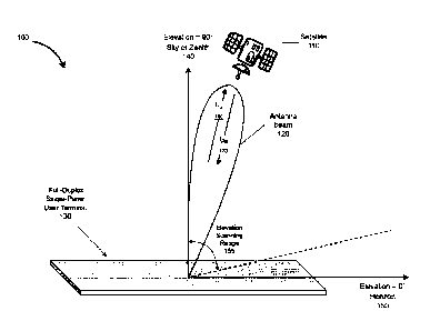
[18] FIG. 1 illustrates a general overview of a full-duplex communication
between a full-
duplex single-panel user terminal and a satellite, according to some
embodiments.
[19] FIG. 2 depicts a block diagram illustrating a full-duplex single-panel
user terminal for
use in full-duplex communication, according to some embodiments.
[20] FIG. 3A depicts a Low Noise Amplifier (LNA) 300a with an input and an
output, according
to some embodiments.
[21] FIG. 3B is a graph illustrating the relationship between the power output
of an LNA and
the power input of the LNA, according to some embodiments.
[22] FIG. 4 is a graph illustrating the RF power vs. Frequency, according to
some embodiments.
[23] FIG. 5 is a graph illustrating the RF power and Noise floor vs.
Frequency, according to
some embodiments.
[241 FIG. 6A-6C depict block diagrams illustrating the single-panel full-
duplex user terminal
for use in full-duplex communication, according to some embodiments.
Page 7 of 63
Date recite/Date received 2023-03-10
Attorney Docket No. 118611.PG454US
[25] FIG. 7A and FIG. 7B contrasts the full-duplex dual-aperture antenna panel
against the full-
duplex single-aperture antenna panel, according to some embodiments.
[26] FIG. 8 illustrates the area projected by a UTP with respect to a
satellite location, according
to some embodiments.
[27] FIG. 9 is a graph illustrating antenna spacing requirement for having a
grating lobe-free
region, according to some embodiments.
[28] FIG. 10 shows an example graph illustrating the effect of a grating lobe
on the full-duplex
antenna system scan performance, according to some embodiments.
[29] FIG. 11A illustrates top views of several configurations of antenna
lattice used by full-
duplex antenna systems, according to some embodiments.
[30]
FIG. 11B illustrates cross-sectional views of several configurations of
antenna lattice used
by full-duplex antenna systems, according to some embodiments.
[31] FIG. 12 illustrates a block diagram of the Transmit (Tx) Radio Frequency
Integrated
Circuit (RFIC), Receive (Rx) RFIC as well as Full-Duplex Antenna Element,
according to
some embodiments.
[32] FIG. 13 is a graph illustrating S-parameters vs. frequency of a full-
duplex antenna element,
according to some embodiments.
[33] FIG. 14 is a graph illustrating realized gain vs. frequency of a full-
duplex antenna element,
according to some embodiments.
[34] FIG. 15 is a graph illustrating S-parameters vs. frequency of a full-
duplex antenna element
utilizing filters, according to some embodiments.
Page 8 of 63
Date recite/Date received 2023-03-10
Attorney Docket No. 118611.PG454US
[35] FIG. 16 depicts an example lattice configuration of a full-duplex antenna
element,
optimized for scanning in the Tx frequency, according to some embodiments.
[36] FIG. 17 depicts an example lattice configuration of a full-duplex antenna
element,
optimized for scanning in the Rx frequency, according to some embodiments.
[37] FIG. 18 depicts an example lattice configuration of a full-duplex antenna
element,
optimized for scanning in the Rx frequency, according to some embodiments.
[38] FIG. 19A depicts a full-duplex antenna element showing a keepout region,
according to
some embodiments.
[39] FIG. 19B illustrates the height of the PCB of the full-duplex antenna
element, according to
some embodiments.
[40] FIG. 20 is a graph illustrating the effect of the keepout region and port
orthogonality,
according to some embodiments.
[41] FIG. 21 depicts the Electric Field intensity of a full-duplex antenna
element, according to
some embodiments.
[42] FIG. 22 is a graph illustrating the S-parameters of a full-duplex antenna
element, according
to some embodiments.
[43] FIG. 23A illustrates a repeating antenna structure and a neighboring
repeating antenna
structure, according to some embodiments.
[44] FIG. 23B is a graph illustrating the S-parameters of a full-duplex
antenna element,
according to some embodiments.
Page 9 of 63
Date recite/Date received 2023-03-10
Attorney Docket No. 118611.PG454US
[45] FIG. 24 is a graph illustrating the scan performance of a full-duplex
antenna element,
according to some embodiments.
[46] FIG. 25A illustrates a top view of a sub-User Terminal Module (UTM),
according to some
embodiments.
[47] FIG. 25B illustrates a cross-sectional view of a sub-UTM, according to
some embodiments.
[48] FIG. 26 illustrates the use of sequentially rotating (SQR) ports in an
antenna array,
according to some embodiments.
[49] FIG. 27 illustrates the use of orthogonal ports and SQR in an antenna
array, according to
some embodiments.
[50] FIG. 28A illustrates a sub-UTM with conventional port placement,
according to some
embodiments.
[51] FIG. 28B illustrates a sub-UTM with SQR port placement, according to some
embodiments.
[52] FIG. 29 illustrates the use of orthogonal ports in a sub-UTM, according
to some
embodiments.
[53] FIG. 30 is a graph illustrating a directivity of an example 2x2 array
when configured in an
SQR vs. conventional port arrangement, according to some embodiments.
[54] FIG. 31 is a graph illustrating axial ratio of an example 2x2 array when
configured in an
SQR vs. conventional port arrangement, according to some embodiments.
[55] FIG. 32 is a graph illustrating a directivity of an example 1x4 array
when configured in an
SQR vs. conventional port arrangement, according to some embodiments.
Page 10 of 63
Date recite/Date received 2023-03-10
Attorney Docket No. 118611.PG454US
[56] FIG. 33 illustrates an antenna element in the presence of a scatterer,
according to some
embodiments.
[57] FIG. 34 illustrates a method of designing an antenna element in the
presence of a scatterer,
according to some embodiments.
[58] FIG. 35 is a graph of a radiation pattern of a full duplex antenna
element, according to
some embodiments.
[59] FIG. 36 depicts a user terminal module, according to some embodiments.
[60] FIG. 37 depicts an example antenna lattice configuration of a full-duplex
single-panel user
terminal panel (UTP), according to some embodiments.
[61] FIG. 38 depicts a top view of an alternate example antenna lattice
configuration of a full-
duplex single-panel user terminal panel (UTP), according to some embodiments.
[62] FIG. 39 depicts a perspective view of an alternate example antenna
lattice configuration of
a full-duplex single-panel user terminal panel (UTP), according to some
embodiments.
[63] FIG. 40 depicts an example antenna lattice configuration of a full-duplex
single-panel user
terminal panel (UTP) using reduced Tx antenna elements, according to some
embodiments.
[64] FIG. 41 depicts another example antenna lattice configuration of a full-
duplex single-panel
user terminal panel (UTP) using reduced Tx antenna elements, according to some
embodiments.
[65] FIG. 42 depicts a UTP with Tx/Rx UTMs and Tx Only UTMs, according to some
embodiments.
Page 11 of 63
Date recite/Date received 2023-03-10
Attorney Docket No. 118611.PG454US
[66] FIG. 43 depicts a UTP with Tx/Rx UTMs and Rx Only UTMs, according to some
embodiments.
[67] FIG. 44 depicts a multi-UTP for Improved Link Performance, according to
some
embodiments.
[68] FIG. 45 depicts a multi-UTP for Improved G/T performance, according to
some
embodiments.
[69] FIG. 46 depicts using multiple UTPs on an airplane fuselage, according to
some
embodiments.
[70] FIG. 47 depicts a block diagram illustrating an example modular
architecture of a full-
duplex single panel user terminal formed with multiple UTMs, according to some
embodiments.
[71] FIG. 48 depicts a block diagram illustrating an example UTM with 9 Tx
RFICs connected
in a daisy chain as well as 4 Rx RFICs connected in a daisy chain, and a
control circuit,
according to some implementations.
[72] FIG. 49 depicts a block diagram illustrating an example control circuit
and four UTMs
connected in a daisy chain.
[73] The drawings have not necessarily been drawn to scale. Similarly, some
components and/or
operations may be separated into different blocks or combined into a single
block for the
purposes of discussion of some of the embodiments of the present technology.
Moreover, while
the technology is amenable to various modifications and alternative forms,
specific
embodiments have been shown by way of example in the drawings and are
described in detail
Page 12 of 63
Date recite/Date received 2023-03-10
Attorney Docket No. 118611.PG454US
below. The intention, however, is not to limit the technology to the
particular embodiments
described. On the contrary, the technology is intended to cover all
modifications, equivalents,
and alternatives falling within the scope of the technology as defined by the
appended claims.
DETAILED DESCRIPTION
[74] Examples are discussed in detail below. While specific implementations
are discussed, it
should be understood that this is done for illustration purposes only. A
person skilled in the
relevant art will recognize that other components and configurations may be
used without
parting from the spirit and scope of the subject matter of this disclosure.
The implementations
may include systems, processes, apparatuses, machine-implemented methods,
computing
devices, or computer readable medium.
[75] As used herein, a user terminal can also be referred to as an antenna
system or UTP. A
single-panel full-duplex user terminal can also be referred to as a single-
panel full-duplex
antenna system. Additionally, a single-panel full-duplex user terminal can be
referred to as a
single-aperture full-duplex user terminal, single-aperture full-duplex antenna
system, or a
single-aperture full-duplex panel.
[76] In a full-duplex satellite communication scenario, at least some of the
power of the Tx
signal can be coupled into the receive portion of the circuitry. Transmitted
signals are typically
transmitted at fairly high power levels. Received signals, however, are
typically received at
much lower power levels than that of the transmitted signals' power levels.
The coupled Tx
signal power into the Rx signal chain can be greater than a noise floor of the
LNA of the Rx
signal, thereby interfering with the Rx signal being reliably received.
Furthermore the coupled
Tx signal power into the Rx signal chain can affect the linear (a.k.a. small-
signal) region of the
Page 13 of 63
Date recite/Date received 2023-03-10
Attorney Docket No. 118611.PG454US
LNA. Reducing Tx/Rx coupling (or improving the Tx/Rx isolation) can improve
the integrity
of the received signal during full-duplex operation. One or more embodiments
described
herein, among other benefits, solve one or more of the foregoing problems in
the art by
providing full-duplex antenna systems and isolation methods to reduce coupling
from a Tx
signal path onto an Rx signal path, and to thereby enable full-duplex
communication and in
certain scenarios enhance full-duplex communication.
[77] In one embodiment, a full-duplex antenna system includes a controller
circuit, a transmit
signal path including one or more elements each including a distribution
network, a Tx RFIC
including one or more power amplifiers (PA), one or more filters, one or more
Tx antenna
element ports of a Tx antenna element operating at a Tx frequency band to
transmit an outgoing
signal to a satellite. The example full-duplex antenna system further includes
an Rx signal path
in the one or more elements, the Rx signal path including a distribution
network, an Rx RFIC
including one or more LNAs driven by an Rx antenna element port of an Rx
antenna element
operating at an Rx frequency band to receive an incoming signal from the
satellite. The Rx
frequency band is separated by a frequency guard band from the Tx frequency
band, and the
filters together with the isolation methods described between the Tx and Rx
signal paths
provides sufficient isolation to reduce coupling between the Tx signal path
and the Rx signal
path to allow the satellite antenna to operate in full-duplex.
[78] In some embodiments, the incoming signal from a satellite is referred to
as an incoming
analog signal or incoming RF signal and the outgoing signal to a satellite is
referred to as
outgoing analog signals or outgoing RF signal. In other embodiments, the
incoming signal
Page 14 of 63
Date recite/Date received 2023-03-10
Attorney Docket No. 118611.PG454US
from a satellite is referred to as a downlink signal and the outgoing signal
to a satellite is
referred to as an uplink signal.
[79] FIG. 1 illustrates a full-duplex single-panel user terminal panel (UTP)
100 communicating
with a satellite 110 using a transmit frequency (a.k.a., uplink) frx 160 and a
receive frequency
(a.k.a. downlink) fRx 170 simultaneously. According to some embodiments, frx
and fRx are
different frequency bands. As an example the Ka band used in satellite
communications uplink
uses frequencies between 27.5 GHz and 30 GHz and the downlink uses frequencies
between
17.7 GHz and 20.2 GHz, employing a Tx frequency to Rx frequency ratio of 3:2
[80] It is to be noted that antenna beam 120 is an illustration of the
transmit frequency antenna
beam and receive frequency antenna beam. In reality the Tx antenna beam and
the Rx antenna
beam may be separate.
[81] The satellite 110 location may be directly above the full-duplex single-
panel user terminal
130 at an elevation angle (EL) of 90 degrees which is directly up towards the
sky 140, at EL =
0 degrees towards the horizon 150, or anywhere in between. The full-duplex
PAsingle-panel
user terminal may be capable of a certain elevation scanning range 155. The
satellite 110 may
be a low earth orbit (LEO) satellite, a geostationary earth orbit (GEO)
satellite, or medium
earth orbit (MEO) satellite.
[82] The full-duplex single-panel UTP may be on a static object such as a roof
of a house or on
a moving platform such as a train, bus, or an airplane.
[83] FIG. 2 is a block diagram illustrating the Tx and Rx signal chains
leading to a full-duplex
antenna element 220, for use in full-duplex communication 200, according to
some
embodiments.
Page 15 of 63
Date recite/Date received 2023-03-10
Attorney Docket No. 118611.PG454US
[84] Transmit/Receive Signal Paths: As shown, antenna element block diagram
200 includes a
transmit signal path, which includes, connected in order, a Tx port 230 (to
receive an analog
input from a modem of a user device), a Tx distribution network 232 (the Tx
distribution
network may be referred to as a Tx splitter), PA 234, a Tx Filter 236,
connected to a Tx antenna
element 222 via a Tx antenna element port 224. As used herein, the Tx port 230
is an analog
input from a user device such as a transceiver into the antenna system. Also
shown is a receive
signal path includes, connected, in order, Rx antenna element 226, connected
via Rx antenna
element port 228 to an Rx Filter 246, which drives LNA 244, which drives RF
distribution
network 242 (the Rx distribution network may also be referred to as an Rx
combiner), which
drives an Rx port 240 to provide as an analog output to a user device such as
a transceiver. Tx
filter 236 and Rx filter 246 may be either a surface mount (SMT) filter or a
PCB-based filter.
[85] As used herein, the PA 234 is a Tx RFIC with one or more Tx channels, and
the LNA 244
is an Rx RFIC with one or more Rx channels.
[86] In some embodiments, the one or more Tx distribution network in the Tx
signal path is also
referred to as a corporate network. In other embodiments, the one or more Rx
distribution
networks in the Rx signal path may be referred to as a corporate network.
[87] As used herein an antenna port is a physical interface on the antenna
that allows for
exchange of RF energy between the antenna and the RF signal path. As an
example, the Tx
antenna port 224 is a physical interface that allows for energy to be
transferred from the PA
into the Tx antenna element. An antenna port is an integral part of the
antenna element and
may be connected with another RF device through an RF transition (not shown)
or through an
Page 16 of 63
Date recite/Date received 2023-03-10
Attorney Docket No. 118611.PG454US
RF coaxial connector (also not shown), such as sub-miniature push-on (SMP),
subminiature
push-on micro (SMP-M), subminiature push-on sub-micro (SMP-S).
[88] As shown in block diagram 200, a Tx/Rx isolation 250 is the isolation
level between a Tx
antenna port and an Rx antenna port. Furthermore, Tx PA/Rx LNA isolation 255
is the isolation
between the PA 234 and the LNA 244. It is to be noted that when deriving full-
duplex isolation
specifications, both Tx/Rx isolation 250 and Tx PA/Rx LNA isolation 255 have
to conform to
said full-duplex specifications.
[89] The full-duplex antenna element 220 as used herein contains at least one
Tx antenna
element 222 and one Rx antenna element 226. In other embodiments, not shown,
more than
one Tx or Rx antenna elements may be used. In other embodiments, also not
shown, a full-
duplex single-panel user terminal contains more Tx antenna elements than Rx
antenna
elements. To support additional Tx antenna elements, additional Tx signal
paths may be used.
[90] In other embodiments, not shown, a full-duplex single-panel user terminal
contains more
Rx signal chains than Tx signal chains. In order to support additional Rx
signal chains, an Rx
antenna element is used in lieu of a full-duplex antenna element.
[91] FIG. 3A depicts an LNA 310 with a power input 320 and a power output 330.
[92] PldB or 1 dB compression point is an output power level at which the gain
of the LNA
decreases 1 dB from the theoretical response 390. Once an amplifier reaches
this PldB it goes
into compression and exhibits non-linear behavior, producing distortion,
harmonics and
intermodulation products. Amplifiers such as LNAs should be operated below the
compression
point, in their linear region.
Page 17 of 63
Date recite/Date received 2023-03-10
Attorney Docket No. 118611.PG454US
[931 FIG. 3B is a graph that illustrates the power output of LNA 330 vs. power
input of LNA
320. Shown are two regions that define the operation of the LNA: a linear
region 340 and a
compression region 350. Furthermore, the graph illustrates the potential
response of the LNA
with a Tx blocker 370 different from the actual response of the LNA without a
Tx blocker 360.
The Tx blocker power 210 (FIG. 2) represents an amount of power in the Tx-band
at the output
of the PA that could couple into the input of the LNA 245 (FIG. 2). When this
happens, the
PldB of the LNA with Tx blocker 385 reduces from a value PldB of LNA without
Tx blocker
380.
[94] A lower input PldB such as depicted in PldB of the LNA with Tx blocker
385 means a
reduced linear region of the LNA 340, which can cause the LNA to output a less
desired (lower)
Signal-to-Noise ratio (SNR). SNR is the ratio of RF signal to RF noise. The
lower the SNR,
the more noise is generated by the receiver.
[951 FIG. 4 is an example graph 400 that illustrates the RF power in dBm 410
vs. frequency
420. By design, the highest level of RF signal 430 in the Rx-band 440 happens
at fRx 470 which
is higher than a noise floor of LNA 450. In addition, the highest level of a
Tx signal 460 in the
Tx band 490 happens at frx 480. A Tx PA skirt power 460 is a byproduct of the
Tx signal
outside of the Tx-band and may affect the Rx signal within the Rx-band if the
Tx PA skirt
power is higher than the noise floor of the LNA 450.
[96] As used herein, the Tx PA skirt power may also be referred to as Tx
skirt.
[97] FIG. 5 is a graph 500 illustrating RF power 510 vs. Frequency 520. As
shown, the noise
floor of LNA without Tx PA 550 in the Rx-band 530 is at a lower level compared
with the
noise floor of LNA in presence of Tx PA 540 in the Rx-band 530. The increase
of the noise
Page 18 of 63
Date recite/Date received 2023-03-10
Attorney Docket No. 118611.PG454US
power in the noise floor of LNA in presence of PA 540 is due to the noise
power that the PA
adds to the existing noise floor of LNA without Tx PA 550, in the Rx-band 530
which is
centered around an Rx frequency fc 560.
[98] FIG. 6A depicts a block diagram illustrating the single-panel full-duplex
user terminal for
use in full-duplex communication, according to some embodiments. Block diagram
600a
shows a more simplified version of the block diagram 200 (FIG. 2). Block
diagram 600a
considers the Tx signal as a blocker and a source of Rx signal interference.
Furthermore, Tx-
band isolation 615 is one example of Tx/Rx isolation 250 (FIG. 2).
[99] In order to operate in full-duplex mode, the Tx-band isolation 615 needs
to be greater than
the absolute value { Tx signal power (Pblocker) in the Tx band at the output
of the PA 610 minus
a power level in the Tx band that would contribute to compressing the LNA by 1
dB in the Rx
band (PidB,blocker) 385 (FIG. 3B)}
[100] Equation 1: Tx-band isolation > I Pblocker - PldB,blocker I
[101] Note that Equation 1 applies if Pblocker > PldB,blocker, otherwise Tx-
band isolation is not
needed.
[102] FIG. 6B depicts a block diagram illustrating the single-panel full-
duplex user terminal for
use in full-duplex communication, according to some embodiments. Block diagram
600b
shows a more simplified version of the block diagram 200 (FIG. 2). Block
diagram 600b
considers the Tx PA skirt power in the Rx-band (FIG. 4) at the output of the
PA 650 as a source
of Rx signal interference. Furthermore, Rx-band isolation 655 is one example
of Tx/Rx
isolation 250 (FIG. 2).
Page 19 of 63
Date recite/Date received 2023-03-10
Attorney Docket No. 118611.PG454US
[103] In order to operate in full-duplex mode, the Rx-band isolation 655 needs
to be greater than
the absolute value of {Tx PA skirt power (Pstia ,PA) in the Rx band at the
output of the PA 650
minus the noise floor of the LNA in the Rx band (Pnoise floor, LNA) I
[104] Equation 2: Rx-band isolation > I Psknt, PA - Pnoise floor, LNA I
[105] Note that Equation 2 applies if Psknt, PA > Pnoise floor, LNA, otherwise
Rx-band isolation is not
needed.
[106] FIG. 6C depicts a block diagram illustrating the single-panel full-
duplex user terminal for
use in full-duplex communication, according to some embodiments. Block diagram
600c
shows a more simplified version of the block diagram 200 (FIG. 2). Block
diagram 600c
considers the Tx noise power in the Rx-band at the output of the PA 670 as a
source of Rx
signal interference. Furthermore, Rx-band isolation 675 is one example of
Tx/Rx isolation 250
(FIG. 2).
[107] In order to operate in full-duplex mode, the Rx-band isolation 675 needs
to be greater than
the absolute value {Tx PA noise power (PnoiseyA) in the Rx band at the output
of the PA 670
minus the noise floor of the LNA in the Rx band}
[108] Equation 3: Rx-band isolation > I Pnoise, PA - Pnolse floor, LNA I
[109] Note that Equation 2 applies if Pnoise, PA > Pnoise floor, LNA;
otherwise Rx-band isolation is not
needed.
[110] FIG. 7A depicts a full-duplex dual-aperture antenna panel 710 consisting
of an Rx antenna
panel 720 and a Tx antenna panel 730. An antenna to antenna separation dRx 740
of the Rx
antenna panel describes a spacing requirement for the operation of the Rx
antenna panel in a
Page 20 of 63
Date recite/Date received 2023-03-10
Attorney Docket No. 118611.PG454US
Rx frequency. An antenna to antenna separation cfrx 750 of the Tx antenna
panel describes a
spacing requirement for the operation of the Tx antenna panel in a Tx
frequency. Combining
the Rx antenna panel and the Tx antenna panel into a full-duplex single
aperture panel 760
(FIG. 7B) for simultaneous operation in the Tx-band and the Rx-band presents
additional
design challenges and requires a new array solution. The antenna elements and
the way they
repeat are no longer preserved. Furthermore, the antenna ground for Tx antenna
elements and
Rx antenna elements is shared. As an example, the Tx antenna elements (assumed
to be above
the Rx antenna elements) are separated by a dielectric layer(s) from the Rx
antenna elements,
while sharing the same ground. Coupling between Tx antenna element 765 and Rx
antenna
element 766 is introduced. Furthermore, instead of routing RF signals from Tx
RFICs into a
Tx antenna panel and similarly routing RF signals from Rx RFICs into an Rx
antenna panel,
the routing of RF signals from Tx RFICs and RF signals from Rx RFICs into the
same panel
is now required, increasing RFIC density.
[111] As used herein, RFIC density is the percentage of a PCB surface area
that will be covered
in RFICs. Furthermore, this is defined as (Area required by one RFIC x Number
of RFICs) /
PCB surface Area.
[112] FIG. 8 depicts a satellite 820 and satellite 825 shown with respect to a
UTP 810. In some
embodiments, satellite 820 and satellite 825 lie in an orbit, like LEO or GEO
and UTP 810 lies
on an Earth surface. As used herein, the term broadside is when the direction
of radiation of
the UTP is perpendicular to its main surface area. In 800, satellite 820 is at
broadside (or 00 =
0 degrees) with respect to UTP 810 and satellite 825 is at an angle 00 * 0
degrees. In some
Page 21 of 63
Date recite/Date received 2023-03-10
Attorney Docket No. 118611.PG454US
embodiments, an elevation (EL) = 90 degrees is equivalent to 00 = 0 degrees,
and an EL = 0
degrees is equivalent to 00 = 90 degrees.
[113] As shown in 800, the UTP Area projected towards a satellite varies in
accordance with 00
of the satellite. The area projected AUTP projected towards a satellite is
equivalent to the area of
the UTP AUTP multiplied by the cosine of the angle 00. As shown, the maximum
AUTP projected is
when the satellite is at 00 = 0 degrees (broadside) with respect to the UTP.
Furthermore, the
gain of the antenna of the UTP (Gulp) referenced at an angle 00 is
proportional to the AUTP
protected and is a maximum when 00 = 0 degrees. In some embodiments, the gain
of the antenna
of the UTP is referred to as the gain of the UTP or GUTP.
[114] Equation 4: AUTP projected = AUTP COS(00)
[115] FIG. 9. is a graph illustrating the grating lobe free requirement 910 on
the antenna to
antenna spacing 920 in terms of wavelength (or free space lambda )). Grating
lobes are
secondary main lobes or very strong side lobes which could be approximately
the size of the
main lobe in an antenna radiation pattern. Grating lobes occur as a result of
spacing among the
antenna elements in the phased array antenna. The objective is to avoid
grating lobes by using
the optimal spacing of antenna elements. As used herein, the antenna to
antenna spacing (or
spacing of antenna elements) is referred to as da. The da requirement shown in
900 is critical
on the scan performance. As an example, a &X = 0.7 is needed to meet the
criteria of free
grating lobes down to a 00= 25 degrees.
[116] FIG. 10. is a graph illustrating the effect of antenna spacing (d/X) =
0.536 on the scan
performance of the UTP. As used herein, scan loss is referred to as scan
performance and is
depicted by a normalized realized gain of the UTP 1020. Graph 1000 shows the
onset of grating
Page 22 of 63
Date recite/Date received 2023-03-10
Attorney Docket No. 118611.PG454US
lobe 1030 around a scan angle (00) of 60 degrees. It is to be noted that in
addition to the grating
lobe free requirement 910 (FIG 9), there exists other considerations that
affect the scan loss,
such as interaction between antenna elements (a.k.a. mutual coupling). Graph
1000 also shows
an ideal power of cosine to the power of 1 1010, which indicates a maximum UTP
gain
achieved.
[117] FIG. 11A and FIG. 11B depict top views and cross sectional views of four
lattice
configurations for a full-duplex single-panel UTP respectively.
[118] Lattice A 1110 has a da configured at a Tx frequency higher than an Rx
frequency. A
combination of a Tx antenna element 1112 with an Rx antenna element 1114
creates a
repeating antenna structure 1115. As used herein, the repeating antenna
structure 1115 is also
referred to as a full-duplex antenna element. Lattice A uses a Tx antenna
element spacing drrx
1152 (FIG. 11B) that is equal to an Rx antenna element spacing dRx 1154.
[119] As used herein, lattice A 1150 uses Tx antenna elements 1158 on a
separate plane than Rx
antenna elements 1156.
[120] Lattice B top view 1120 and cross sectional view 1160 has two
configurations B-1 and B-
2. B-1 1165 (FIG. 11B) and B-2 1167 (FIG. 11B) have their dA, configured at an
Rx frequency
lower than a Tx frequency. B-1 uses a Tx antenna element spacing drrx 1162
that is equal to an
Rx antenna element spacing dRx 1164. B-2 uses a Tx antenna element spacing
drrx 1168 that is
equal to an Rx antenna element spacing dRx 1166. As shown in B-1 1122, a
combination of a
Tx antenna element 1123 with an Rx antenna element 1124 creates a repeating
antenna
structure 1125. As used herein, the repeating antenna structure 1125 is also
referred to as a
full-duplex antenna element. As shown in B-2 1126, a combination of a Tx
antenna element
Page 23 of 63
Date recite/Date received 2023-03-10
Attorney Docket No. 118611.PG454US
1128 with an Rx antenna element 1127 creates a repeating antenna structure
1129. As used
herein, the repeating antenna structure 1125 is also referred to as a full-
duplex antenna element.
[1211 As used herein, lattice B-1 1165 uses Tx antenna elements 1121 on a
separate plane than
Rx antenna elements 1163. lattice B-2 1167 uses Tx antenna elements 1169 on
the same plane
as Rx antenna elements 1190.
[1221 Lattice C 1130 is an example of a lattice configured to meet
specifications of da for a Tx
frequency as well as an Rx frequency. As used herein, the Tx frequency is
higher than the Rx
frequency. In other embodiments, Rx frequency is higher than a Tx frequency.
[1231 Lattice C cross-sectional view 1170, shows using a Tx antenna element
spacing &a 1172
different from Rx antenna element spacing dRx 1174. For a square UTP, the side
dimension D
1176 for Lattice C 1170 that would make it a repeating antenna structure 1135
is the maximum
of the two values: Md.Tx and NdRx where M is the number of Tx antenna elements
and N is the
number of Rx antenna elements. As used herein, a repeating antenna structure
1135, is a
repeating pattern that allows for the scaling of the UTP by multiplying the
number of repeating
antenna structures in a KxK fashion, where K is an integer number.
[1241 Equation 5: D=max(MdTx,NdRx)
[1251 As used herein, lattice C 1170 uses Tx antenna elements 1171 on a
separate plane than Rx
antenna elements 1173.
[1261 Lattice D 1140 is another example of a lattice configured to meet
specifications of da for
a Tx frequency as well as an Rx frequency. As used herein, the Tx frequency is
higher than the
Rx frequency. In other embodiments, Rx frequency may be higher than a Tx
frequency.
Page 24 of 63
Date recite/Date received 2023-03-10
Attorney Docket No. 118611.PG454US
[127] Lattice D-1 top view 1142 and D-2 top view 1144, both show using a Tx
antenna element
spacing d:rx 1182 different from Rx antenna element spacing dRx 1184.
[128] In some embodiments, the side dimension D 1185 for Lattice D1 1142 that
would make it
a repeating antenna structure 1146 in a square configuration is the maximum of
the two values:
nth'', and NdRx where M is the number of Tx antenna elements and N is the
number of Rx
antenna elements. As used herein, a repeating antenna structure 1146, is a
repeating pattern
that allows for the scaling of the UTP by multiplying the number of repeating
antenna
structures in a KxK fashion, where K is an integer number.
[129] In other embodiments, the side dimension D 1185 for Lattice D2 1144 that
would make it
a repeating antenna structure 1148 in a square configuration is the maximum of
the two values:
MdTx and NdRx where M is the number of Tx antenna elements and N is the number
of Rx
antenna elements. As used herein, a repeating antenna structure 11468, is a
repeating pattern
that allows for the scaling of the UTP by multiplying the number of repeating
antenna
structures in a KxK fashion, where K is an integer number.
[130] As used herein, lattice D-1 and D-2 both use Tx antenna elements 1181 on
a separate plane
than Rx antenna elements 1183.
Table 1. Pros and Cons of Lattice Configurations
Lattice Pros Cons
A = No grating lobes for both = Highest RFIC density
Tx and Rx frequencies = Highest DC power that is
(and therefore an required to drive the RFICs
optimum scanning) = Cost is highest due to the
depending on value of highest RFIC density
separation with respect to = Highest coupling between any
Page 25 of 63
Date recite/Date received 2023-03-10
Attorney Docket No. 118611.PG454US
Tx wavelength (d/X) two adjacent Rx antenna
= Repeating antenna
elements due solely to their
structure consists of 1 smallest spacing
type of antenna
comprising a Tx antenna
element and an Rx
antenna element
B-1 = Minimum RFIC density = Presence of grating lobes in
the
= Repeating antenna Tx
frequencies and therefore
structure consists of a highest scan loss in the Tx
single type of full-duplex frequency
antenna element
comprising a Tx antenna
element disposed above
an Rx antenna element
B-2 = Minimum RFIC density = Presence of grating lobes in
the
= Repeating antenna Tx
frequencies and therefore
structure consists of a highest scan loss in the Tx
single type of full-duplex frequency
antenna element
comprising a Tx antenna
element disposed
diagonal with respect to
an Rx antenna element,
resulting in a more cost
effective PCB
manufacturing
= No grating lobes for both =
Requires 2 different types of
Tx frequency and Rx antenna elements (for the
frequency (and therefore example of Ka band where
the
an optimum scanning) , ratio of Tx to Rx frequency
is
depending on value of 3:2) within the repeating
separation with respect to antenna structure, this
means:
wavelength for each Tx single band Tx antenna
element
(d/TA) and Rx (d/X), and a dual band Tx/Rx
element
chosen separately
D1 = No grating lobes for both = Requires 3 different types
of
Tx frequency and Rx antenna elements (for the
Page 26 of 63
Date recite/Date received 2023-03-10
Attorney Docket No. 118611.PG454US
frequency (and therefore example of Ka band where
the
an optimum scanning) , ratio of Tx to Rx frequency
is
depending on value of 3:2) within the repeating
separation with respect to antenna structure, this
means:
wavelength for each Tx single band Tx antenna
element,
(d/TA) and Rx (d/)), single band Rx antenna
chosen separately element, and a dual band
Tx/Rx
element
D2 = No grating lobes for both = Requires 2 different
types of
Tx frequency and Rx frequency antenna elements (for the
(and therefore an optimum example of Ka band where
the
scanning) , depending on value of ratio of Tx to Rx frequency
is
separation with respect to 3:2) within the repeating
wavelength for each Tx (d/)) and antenna structure, this
means:
Rx (d/X), chosen separately single band Tx antenna
element
= Lower in cost compared
and a single band Rx antenna
with D1 because it uses less Tx element
antenna elements and therefore
less Tx RFICs
[131] FIG. 12 depicts a block diagram 1200 showing the Tx RFIC 1210 channels
such as Ch Ti
1211, Ch T2 1212 connected to a Tx antenna element 1230 through port Ti 1231
and port T2
1232, respectively. Also shown in 1200 are the connections between an Rx RFIC
1220
channels Ch R1 1221, Ch R2 1222 connected to an Rx antenna element 1230
through port R1
1233 and port R2 12324, respectively. As shown, the full-duplex antenna
element 1230 has a
total of 4 ports, with 2 ports per Tx antenna element and 2 ports per Rx
antenna element. The
2 ports per Tx and Rx antenna elements allow for full polarization control. As
shown in 1200,
Ch Ti 1211 is connected to port Ti 1231 of the full-duplex antenna element
1230, Ch T2 1212
is connected to port T2 1232 of the full-duplex antenna element 1230, Ch R1
1221 is connected
to port R1 1233 of the full-duplex antenna element 1230, and Ch R2 1222 is
connected to port
R2 1234 of the full-duplex antenna element 1230. In some embodiments, Ch T3
1213, Ch T4
Page 27 of 63
Date recite/Date received 2023-03-10
Attorney Docket No. 118611.PG454US
1214, Ch R3 1223, and Ch R4 1224 are connected to another full-duplex antenna
element (not
shown). In other embodiments (not shown), the Tx RFIC 1210 and the Rx RFIC
1220 may
have 1 channel, 2 channels, 8 channels, or 16 channels.
[132] Shown in FIG. 12 are the self S-parameters STI,T1 1260, ST2,T2 1265,
SR1,R1 1270, SR2,R2
1275 which represent an energy reflected at the respective port. As an
example, ST1,T1
represents an amount of power that is reflected at port Ti. As used herein, a
self S-parameter
is referred to as return loss.
[133] Also shown in FIG. 12 are the mutual S-parameters SR2,T1 1240, SR1,Ti
1243, SR1,T2 1245,
SR2,T2 1247 which represent an energy coupled from one port to another in the
network that is
shown in the block diagram 1200. As an example, SR1,T1 represents an amount of
power that
is coupled from port Ti into port Rl. As used herein, a mutual S-parameter is
referred to as
coupling.
[134] FIG. 13 is a graph that illustrates a threshold level for return loss
and coupling, according
to some embodiments. Graph 1300 shows a vertical axis 1310 that represents an
amplitude of
the S-matrix in decibel [dB] and a horizontal axis that has the frequency
1320, typically in
units of GHz. Also shown are specific frequencies of interest such as fRx 1360
and frx 1370.
[135] In some embodiments SR1,R1 1342 is an example of a return loss of a Rx
antenna element
of a full duplex antenna element and STI,T1 1344 is an example of a return
loss response of a
Tx antenna element of a full-duplex antenna element. Furthermore, SR1,T1 1346
is an example
coupling response between a Tx antenna element and a Rx antenna element of a
full-duplex
antenna element.
Page 28 of 63
Date recite/Date received 2023-03-10
Attorney Docket No. 118611.PG454US
[136] In some embodiments, a threshold level is defined for the return loss
1352 of a Tx antenna
element and Rx antenna element, as well as a coupling 1354 between a Tx
antenna element
and an Rx antenna element.
[137] FIG. 14 is a graph that illustrates exemplar realized gain measurements
of the Tx antenna
element 1440 of a full-duplex antenna element and realized gain measurements
of the Rx
antenna element 1450 of a full-duplex antenna element, according to some
embodiments. Also
in 1440 are the simulation results of the Tx antenna element 1420 and the
simulation results of
the Rx antenna element 1430. Realized gain is an important antenna metric that
represents the
amount of energy that is accepted by an antenna and radiated out. Graph 1400
shows that at
19.5 GHz, the realized gain of the Rx antenna element is around 5 dB while the
realized gain
of the Tx antenna element is around -25 dB. This difference of 30 dB in the
realized gain
between the Rx antenna element and the Tx antenna element is key to a
successful full-duplex
operation and owes itself to the design of the full-duplex antenna element
including the
isolation between the Tx antenna element and the Rx antenna element.
[138] FIG. 15 is a graph that illustrates the S-parameters response of a full-
duplex antenna
element 220 (FIG. 2) with and without a Tx filter 236 (FIG. 2) and an Rx
filter 246 (FIG 2).
As shown in 1500, the SR1,T1 with filter 1532 presents a significant
improvement when
compared with SR1,T1 without filter 1530. Also shown in 1550 are SR1,R1 with
filter 1510 and
SR1,R1 without filter 1530 as well as ST1,T1 with filter 1520 and ST1,T1
without filter 1522. As
used herein, the Tx filter is a band-pass filter for the Tx frequency range 29
GHz to 31 GHz
and the Rx filter is a band pass filter for the Rx frequency range 17GHz to 20
GHz. The penalty
Page 29 of 63
Date recite/Date received 2023-03-10
Attorney Docket No. 118611.PG454US
of using such filters is the insertion loss that the filter itself adds to the
circuitry, which
ultimately results in a reduced G/T of the UTP and a reduced EIRP of the UTP.
[139] FIG. 16 depicts a UTP with Lattice A (FIG. 11A) which uses a da,
configured at a Tx
frequency higher than an Rx frequency. Lattice A uses a Tx antenna element
spacing drrx 1610
that is equal to an Rx antenna element spacing dRx 1615. As used herein, a
full-duplex antenna
element 1620 consists of a Tx antenna element 1630 and an Rx antenna element
1640.
[140] FIG. 17 depicts a UTP with Lattice B-1 (FIG. 11A) which uses a da,
configured at an Rx
frequency lower than a Tx frequency. Lattice B-1 uses an Rx antenna element
spacing dRx 1710
that is equal to a Tx antenna element spacing d'rx 1715. As used herein, a
full-duplex antenna
element 1720 consists of a Tx antenna element 1730 and an Rx antenna element
1740.
[141] FIG. 18 depicts a UTP with Lattice B-2 (FIG. 11A) which uses a da,
configured at an Rx
frequency lower than a Tx frequency. Lattice B-2 uses an Rx antenna element
spacing dRx 1810
that is equal to a Tx antenna element spacing d'rx 1815. As used herein, a
full-duplex antenna
element 1820 consists of a Tx antenna element 1830 and an Rx antenna element
1840.
[142] FIG. 19A and FIG. 19B illustrate a full-duplex antenna element for
performing full-duplex
communication, according to some embodiments. 1900a illustrates a top view of
a full-duplex
antenna element 1905, including a Tx antenna element keepout region 1915 of a
Tx antenna
element 1910 and an Rx antenna element keepout region 1925 of an Rx antenna
element 1920.
As used herein, the Tx antenna element keepout region is a spatial zone
disposed about a
periphery of the Tx antenna element, and the Rx antenna element keepout region
is a spatial
zone disposed about a periphery of the Rx antenna element. As shown herein,
1905 is an
example of a Tx antenna element 1910 and an Rx antenna element 1920 lying on
an x-y plane
Page 30 of 63
Date recite/Date received 2023-03-10
Attorney Docket No. 118611.PG454US
1940 of a printed circuit board (PCB). In other embodiments, the Tx antenna
element and the
Rx antenna element are disposed on different layers of a PCB. The Tx antenna
keepout region
1915 and the Rx antenna keepout region 1925 are dependent upon the electric
field strength of
the Tx antenna element 1910 and the Rx antenna element 1920, respectively. The
stronger the
electric field strength, the larger the keepout region. The purpose of the Tx
antenna keepout
region and the Rx antenna keepout region plays a key role in maximizing the
Tx/Rx isolation
250 (FIG. 2) within the full-duplex antenna element 1905.
[143] 1900b illustrates a cross-sectional view of a full-duplex antenna
element 1905, according
to some embodiments. In such embodiments, the Tx antenna keepout region and Rx
antenna
keepout region extends beyond the x-y plane 1940 and into the z plane 1950. In
such
embodiments, the Tx antenna element and the Rx antenna element are disposed on
one or more
layers of the PCB 1955.
[144] FIG. 19A also illustrates Tx antenna element port 1913 placed in a non-
orthogonal
orientation when compared with Rx antenna element port 1927. Also shown is Tx
antenna
element port 1917 in an orthogonal orientation when compared with Rx antenna
element port
1927.
[145] FIG. 20 is a graph illustrating the effect of keepout region as well as
port orientation of the
full-duplex antenna element, according to some embodiments. Graph 2000 is an
exemplary
graph illustrating the coupling level between a Tx antenna element port and an
Rx antenna
element port of the full-duplex antenna element of an antenna system. As shown
in graph 2000,
using a keepout region 2020 reduces the coupling level between the Tx antenna
element port
and the Rx antenna element port; in other words the isolation between said
ports increases in
Page 31 of 63
Date recite/Date received 2023-03-10
Attorney Docket No. 118611.PG454US
the frequency range of interest 2050, when compared with a scenario where no
keepout region
was used 2010.
[146] Graph 2000 also illustrates the effect of antenna element port
orthogonality on the isolation
between Tx antenna element and Rx antenna element. As shown, an STx,Rx with
keepout region
and with orthogonal port orientation 2040 shows more isolation than STx,Rx
with keepout region
and without orthogonal port orientation 2020, in a frequency range of interest
2050.
[147] FIG. 21 depicts an Electric Field 2130 of an Rx antenna element 2140 in
presence of a Tx
antenna element 2110 within a full-duplex antenna element 2100, according to
some
embodiments. As illustrated in 2100, a confinement of the Electric Field
strength at the Rx
antenna is due to the Rx antenna element keepout region (not shown). This in
turn, enables a
large isolation between the Rx antenna element port and the Tx antenna element
port. This is
depicted by haying weak Electric Field at the Tx antenna element port (40dB
lower with
reference to the strongest Electric Field at the Rx antenna port) coupled from
the Rx antenna
element port. As used herein, the coupling between an Rx antenna and a Tx
antenna is the same
as the coupling between the Rx antenna port and the Tx antenna port.
[148] FIG. 22 is a graph that illustrates the S-parameters of a full-duplex
antenna element using
Lattice B-2 (FIG. 11A), according to some embodiments. Shown in graph 2200
are: measured
return loss of an Rx antenna element 2210, simulated return loss of an Rx
antenna element
2215, measured return loss of a Tx antenna element 2220, simulated return loss
of a Tx
antenna element 2225, measured isolation between Tx antenna element and Rx
antenna
element 2230, and simulated isolation between Tx antenna element and Rx
antenna element
Page 32 of 63
Date recite/Date received 2023-03-10
Attorney Docket No. 118611.PG454US
2235. The S -parameters are of specific interest in certain bands such as Rx
band 2240 and Tx
band 2250.
[149] FIG. 23A illustrates a repeating antenna structure 2310 and a
neighboring repeating
antenna structure 2315. As used herein, a neigboring repeating antenna
structure is any
repeating antenna structure that is touching 2310.
[150] FIG. 23B is a graph that illustrates the isolation between a Tx antenna
element port of a
unit cell 2310 and neigboring Rx antenna elements of neighboring unit cells,
according to some
embodiments. As used herein, a repeating full-duplex antenna element may also
be referred to
as a unit cell. Graph 2300b show the isolation level between Tx element of
unit cell 2310 and
the Rx antenna element of unit cells 2315, 2316, 2317, 2318, and 2319. Those
unit cells are
chosen due to the smaller proximity of their Rx antenna element with that of
the Tx antenna
element of 2310 and it is assumed that the isolation between the Tx antenna
element 2310 with
the Rx elements of those unit cells that are further away would yield a better
isolation. In
addition, the isolation of the Tx element with the Rx element of unit cell
2310 itself is shown
on graph 2300b. It is noteworthy that the graph of 2300b assumes that there
are an infinite
amount of unit cells, which is a well-accepted practice in the antenna array
discipline when
there are a large number of unit cells, such as tens of unit cells, hundreds,
and even more. As
shown, graph 2300b illustrates that the isolation levels of the Tx antenna
element of the unit
cell 2310 and five Rx antenna elements of neighboring unit cells in the Tx
band 2330 are
comparable to the isolation level of a Tx antenna element and an Rx antenna
element of the
same unit cell, such as the simulated isolation between Tx antenna element and
Rx antenna
element 2235 in FIG. 22.
Page 33 of 63
Date recite/Date received 2023-03-10
Attorney Docket No. 118611.PG454US
[151] In some embodiments, a repeating antenna structure is referred to as a
full duplex antenna
element.
[152] FIG. 24 is a graph that illustrates the scan performance (or scan loss)
for the repeating full-
duplex antenna element 2300a (FIG. 23-A). 2400 is a graph of normalized
realized gain 2405
vs. Theta 2407, representing a single repeating full-duplex antenna element
gain normalized
to a maximum gain value vs. theta. As used herein, the scan loss is the
normalized realized
gain of a full-duplex antenna element. Trace 2410 represents a power of cosine
to the power
of 1; an ideal case of scan loss. Trace 2420 represents the scan loss of the
Rx antenna element.
Trace 2430 represents the scan loss of the Tx antenna element. Graph 2400
takes into account
the effect of all neighboring repeating full-duplex antenna elements. Due to
this, the scan loss
of the full-duplex single panel user terminal is the same as the scan loss of
the full-duplex
antenna element.
[153] FIG. 25A depicts a top view of a sub-UTM and FIG. 25B depicts a cross-
sectional view of
a sub-UTM, according to some embodiments. As referred to herein, a sub-UTM is
the smallest
physically manufacturable PCB; or the smallest building block that is used to
create a larger
UTP. As shown, a sub-UTM 2510 consists of two types of antenna elements: a Tx
antenna
element 2520 and a dual-band Tx/Rx antenna element 2530. Furthermore, as used
herein, there
is no standalone Rx antenna element and the functionality of the Rx antenna
element is a part
of the dual-band Tx/Rx antenna element.
[154] 2500b shows the Tx antenna element to Tx antenna element separation cfrx
2550 is different
from the Rx antenna element to antenna element separation dRx 2560, as
discussed previously
in FIG. 11A and 11B. This different spacing in &a and dRx may provide optimum
scan
Page 34 of 63
Date recite/Date received 2023-03-10
Attorney Docket No. 118611.PG454US
performance for two different frequencies and may result in similar scan
performance for the
Tx and Rx frequency bands as opposed to difference scan performance for the Tx
and Rx
frequencies as shown in FIG. 24.
[155] The side dimension of a square sub-UTM is given by equation 5 above.
[156] FIG. 26 illustrates a method of Sequentially Rotating Feeds (SQR),
according to some
embodiments. The method consists of rotating a 1st antenna element 2620 by 90
degrees with
respect to a z-axis 2617 to create a 2nd antenna element 2630. Furthermore, a
1st port 2622 of
the 1st antenna element 2620 is rotated 90 degrees, with respect to the z-
axis, and a 90 degrees
phase addition is applied to it. For example, 1st port 2622 originally had 90
degrees applied to
it, and after rotating it by 90 degrees with respect to the z-axis, a 180
degrees phase is applied
to it. In a similar way, a 2nd port 2624 of the 1st antenna element is rotated
by 90 degrees
physically to a 2nd port 2634 of the 2nd antenna element 2630, with respect to
the z-axis, and
a 90 degrees phase addition is applied to it. The 2nd antenna element 2630 may
also be seen
as mirrored 1st antenna element 2620 with respect to the y-axis 2615. In a
similar way, the 2nd
antenna element rotates physically by 90 degrees, with respect to a z-axis
2617, creating a 3rd
antenna element 2640. The 3rd antenna element 2640 may also be seen as a
mirrored 2nd
antenna element 2630 with respect to the x-axis 2610. This SQR method is
completed after a
4th antenna element and its ports are created, by rotating a 3rd antenna
element and its ports
by 90 degrees with respect to the z-axis. The principle of SQR hence requires
both physically
rotating the feeds of the antenna element by 90 degrees and changing the
applied phase to each
antenna port via the RFIC. Implementing an SQR configuration achieves an
improvement of
an axial ratio (AR) bandwidth (BW) for each element. The AR is an important
antenna
Page 35 of 63
Date recite/Date received 2023-03-10
Attorney Docket No. 118611.PG454US
parameter especially in circularly polarized antennas and maintaining an AR <
3dB is an
important metric to achieve.
[157] FIG. 27 illustrates an alternate SQR method. As shown in 2700, a 90
degrees physical
clockwise rotation of a 1st antenna element 2720 is applied to create a 2nd
antenna element
2730, in such a way that the 1st port 2722 of the first antenna element 2720
is rotated a 90
degrees clockwise, and an additional 180 degrees physical clockwise rotation,
resulting in a
2nd port location 2734 of the 2nd antenna element 2730. Furthermore, a 180
degrees additional
phase is applied in addition to the original 90 degrees phase addition
described in 2600,
resulting in a total additional phase of 270 degrees to each port.
[158] Both SQR 2600 and alternate SQR 2700 are effective ways to enhance AR
BW.
[159] FIG. 28A depicts a sub-UTM using conventional feeding 2810. As shown,
all Rx antenna
elements of the sub-UTM use a similar orientation of ports such as port A
2815, and port B
2817 of Rx antenna element 2830. In a similar way, all Tx antenna elements of
the sub-UTM
2810 use a similar port orientation as ports 1 2820 and port 2 2825 of Tx
antenna element 2835.
[160] FIG. 28B depicts a sub-UTM with SQR feeding 2850. As shown, ports 3 and
port 4 of Tx
antenna element 2872 employ an SQR feeding method and are hence rotated 90
degrees
clockwise when compared with port 1 and port 2 of Tx antenna element 2870,
respectively.
Furthermore, Tx antenna element 2874 is rotated 90 degrees clockwise with
respect to Tx
antenna element 2872 and Tx antenna element 2876 is rotated 90 degrees
clockwise with
respect to Tx antenna element 2874. A similar SQR feeding method is applied to
the Rx
antenna elements of sub-UTM 2850.
Page 36 of 63
Date recite/Date received 2023-03-10
Attorney Docket No. 118611.PG454US
[161] FIG. 29 depicts a sub-UTM with alternate SQR feeding 2900, according to
some
embodiments. As used herein, SQR method is applied to the Rx antenna elements
and Tx
antenna elements. In this example, the additional 180 degrees rotation that is
applied to the
ports is only used on the Rx antenna ports: port A 2920 of Rx antenna element
2940 is rotated
180 degrees to location A' 2925 and port B 2930 of Rx antenna elements 2940 is
rotated by
180 degrees to location B' 2935.
[162] FIG. 30 is a graph illustrating an example SQR directivity. In this
example three
configurations are compared against each other for a 2x2 microstrip antenna
array resembling
a configuration similar to that shown in FIG. 26 for an SQR feeding and FIG.
27 for an alternate
SQR feeding. For each configuration, the co-pol and the cross-pol directivity
are plotted. As
shown, the co-pol of the conventionally fed array 3010, the co-pol of the SQR
fed array 3020,
and the co-pol of the alternate SQR fed array 3030 are comparable to each
other, varying less
than 0.2 dB in the broadside direction (theta = 0 degrees). The cross-pol of
the conventionally
fed array 3040 is shown to be significantly higher (more than 30 dB) than the
cross-pol of the
SQR fed array 3050 and the cross-pol of the alternate SQR fed array 3060. The
cross-pol is an
antenna metric that is kept low with most antenna system specifications
calling for a value
lower than -20dB.
[163] FIG. 31 is a graph illustrating the broadside AR of the 2x2 SQR
Microstrip Antenna Array
for the conventionally fed array 2910 and the SQR fed array 2920. As shown,
the AR of the
SQR fed array is lower in value compared with the conventionally fed array. In
addition the
AR of the SQR fed array exhibits more flatness when compared with the AR of
the
conventionally fed array.
Page 37 of 63
Date recite/Date received 2023-03-10
Attorney Docket No. 118611.PG454US
[164] FIG. 32 is a graph illustrating another example of SQR directivity. In
this example two
configurations are compared against each other for a 1x4 microstrip antenna
array. For each
configuration, the co-pol and the Cross-pol directivity are plotted. As shown,
the co-pol of the
conventionally fed array 3210 and the co-pol of the SQR fed array 3220 are
comparable to
each other, varying less than 0.1 dB in the broadside direction (theta = 0
degrees). The cross-
pol of the conventionally fed array 3230 is shown to be significantly higher
(more than 30 dB)
than the cross-pol of the SQR fed array 3240.
[165] FIG. 33 illustrates an antenna 3310 with Port 1 settings 3320 of
amplitude and phase and
Port 2 settings 3330 of amplitude and phase. Also shown is a scatterer 3340. A
scatterer is
considered to be any other object in the vicinity of the antenna 3310,
including another antenna.
A coupling 3350 exists between the antenna 3310 and the scatterer 3340. This
coupling 3350
depends on several factors like the size of the scatterer, the distance
between the antenna 3310
and the scatterer 3340 and the material of the scatterer. The coupling 3350
may affect Port 1
setting 3310 and Port 2 setting 3330 and ultimately change the polarization of
a radiated wave
of antenna 3310 and the cross-pol level of antenna 3310.
Table 2. Port excitation to Electric Field Propagation Reference Table
Port Excitation Electric Field Propagation
Port 1 Port 1 Port 2 Port 2 Normalized Normalized Normalized
Normalize
amplitude phase amplitude phase Ex Ex phase Ey d Ey
phase
amplitude amplitude
1 0 0 0 1 0 0 0
1 90 0 0 1 90 0 0
0 0 1 0 0 0 1 0
Page 38 of 63
Date recite/Date received 2023-03-10
Attorney Docket No. 118611.PG454US
0 0 1 90 0 0 1 90
[166] FIG. 34 illustrates a method of removing an effect of a scatterer on the
performance of an
antenna, according to some embodiments. As shown, flow 3400 starts at 3410
with a reference
table such as Table 2, which resembles an ideal case of port excitation to
electric field
propagation. Operation 3420 calls for simulating an antenna with presence of a
scatterer which
could be another antenna. Operation 3420 calls for calculating a Amatrix which
is the difference
between the simulation of the antenna and the reference table. Operation 3440
calls for
applying a function f(Amatrix) to Port 1 and Port 2 settings (amplitude and
phase), which will
bring the antenna to exhibit its ideal values; in other words, f(Amatri x)
will remove the effect of
the scatterer. Furthermore, conditions for circular polarizations may be
applied.
[167] In other embodiments, operation 3420 may be performed in lab
measurements.
[168] FIG. 35 is a graph illustrating a gain pattern of a dual-band Tx/Rx
antenna element 2530
(FIG. 25A). As shown, a Right Hand Circularly Polarized (RHCP) gain plot 3510
is shown at
an Rx frequency of 19 GHz and a Left Hand Circularly Polarized (LHCP) gain
plot 3520 is
shown at a Tx frequency of 29 GHz. It is worth noting that the two gain plots
are orthogonal
to each other, creating an additional polarization discrimination between the
individual Tx and
Rx antenna elements of the dual-band Tx/Rx antenna element.
[169] FIG. 36 depicts a UTM 3600 comprised of four sub-UTMs utilizing SQR
method,
according to some embodiments. As shown, dual band Tx/Rx antenna element 3622
of sub-
UTM 3612 is formed by physically rotating dual band Tx/Rx antenna element 3620
of sub-
UTM 3610 by 90 degrees clockwise. Dual band Tx/Rx antenna element 3624 of sub-
UTM
Page 39 of 63
Date recite/Date received 2023-03-10
Attorney Docket No. 118611.PG454US
3614 is formed by physically rotating dual band Tx/Rx antenna element 3622 of
sub-UTM
3612 by 90 degrees clockwise. Furthermore, dual band Tx/Rx antenna element
3626 of sub-
UTM 3616 is formed by physically rotating dual band Tx/Rx antenna element 3624
of sub-
UTM 3614 by 90 degrees clockwise. Combined, sub-UTM 3610, sub-UTM 3612, sub-
UTM
3614, sub-UTM 3616 form a single UTM. As used herein, a sub-UTM is the
smallest form of
a PCB used as a building block for realizing a UTM.
[170] As shown herein, the center to center spacing dRx 3650 is equal to dRx
3655 of any 2
neighboring Rx antenna elements. Similarly cfrx 3660 is equal to cfrx 3665 of
any two
neighboring Tx antenna elements; wherein cfrx is different than dRx, allowing
for independent
beam scanning in the Tx frequency and Rx frequency simultaneously.
[171] FIG. 37 depicts a UTP 3700 comprised of UTM 3710, UTM 3720, UTM 3730,
and UTM
3740. UTM 3710 may be duplicated horizontally and/or vertically to create a
UTP of any size
of nxn UTMs, where n is an integer, according to some embodiments.
[172] FIG. 38 depicts a top view of UTP 3800 comprised of UTM 3810, UTM 3820,
UTM 3830,
and UTM 3840. Each of the UTM 3810, UTM 3820, UTM 3830, and UTM 3840 are
identical
UTMs. UTM 3810 may be duplicated horizontally and/or vertically to create a
UTP of any
size of nxn UTMs, where n is an integer, according to some embodiments.
Furthermore, each
UTM consists of Tx/Rx configuration 1 3870, Tx/Rx configuration 2 3880, Tx/Rx
configuration 3 3890. Similar to 3600, each of the UTM 3810, UTM 3820, UTM
3830, and
UTM 38340 employ a center to center spacing Rx spacing 3855 that is identical
for any 2
neighboring Rx antenna elements. Similarly a center to center spacing Tx
spacing 3850 of any
two neighboring Tx antenna elements is identical; wherein Rx spacing is
different from Tx
Page 40 of 63
Date recite/Date received 2023-03-10
Attorney Docket No. 118611.PG454US
spacing, allowing for independent beam scanning in the Tx frequency and Rx
frequency
simultaneou sly.
[173] FIG. 39 depicts a perspective view of UTP 3900. As shown, the UTP 3900
comprises a
dielectric group 2 3930 disposed above dielectric group 1 3920. In addition,
UTP 3900
comprises a main ground plane 3910, according to some embodiments.
[174] FIG. 40 depicts a top view of UTP 4000 comprised of UTM 4010, UTM 4020,
UTM 4030,
and UTM 4040. Each of the UTM 4010, UTM 4020, UTM 4030, and UTM 4040 are
identical
UTMs. UTM 4010 may be duplicated horizontally and/or vertically to create a
UTP of any
size of nxn UTMs, where n is an integer, according to some embodiments.
Furthermore, each
UTM consists of Tx/Rx configuration 1 4050, Tx/Rx configuration 2 40550, Rx
configuration
4060. Similar to 3600, each of the UTM 4010, UTM 4020, UTM 4030, and UTM 4040
employ
equal Rx spacing of any two neighboring Rx antenna elements and equal Tx
spacing of any
two neighboring Tx antenna elements with the exception of the removed Tx
antenna
neigboring element; wherein Rx spacing is different from Tx spacing, allowing
for independent
beam scanning in the Tx frequency and Rx frequency simultaneously.
Furthermore, each of
the UTM 4010, UTM 4020, UTM 4030, and UTM 4040 have 1 less Tx antenna element
when
compared to UTM 3600 and/or UTM 3800, resulting in an even number of Tx
antennas per
UTM, according to some embodiments. An even number of Tx antenna elements
requires an
even number of RFIC channels which may be more commercially available than an
odd
number of RFIC channels; albeit at the expense of less Tx antenna radiation.
In some
embodiments, this is referred to as array thinning. The UTP gain is related
directly to the area
of the illuminated aperture, the gain of the UTP will be reduced in
approximate proportion to
Page 41 of 63
Date recite/Date received 2023-03-10
Attorney Docket No. 118611.PG454US
the fraction of the elements removed. However, the UTP beamwidth is related to
the largest
dimension of the single-panel, the removal of elements does not significantly
change its
bearnwidth. This procedure can make it possible to build a highly directive
array with reduced
gain at a lower cost of a filled array.
[175] FIG. 41 depicts a UTM 4100 comprised of four sub-UTMs utilizing SQR
method,
according to some embodiments. As shown, sub-UTM 4120 is formed by physically
rotating
sub-UTM 4110 by 90 degrees clockwise. Sub-UTM 4130 is formed by physically
rotating sub-
UTM 4120 by 90 degrees clockwise. Sub-UTM 4140 is formed by physically
rotating sub-
UTM 4130 by 90 degrees clockwise. Combined, sub-UTM 4110, sub-UTM 4120, UTM
4130,
and sub-UTM 4140 form a single UTM. As used herein, a sub-UTM is the smallest
form of a
PCB used as a building block for realizing a UTM. As shown, each of the sub-
UTM 4110, sub-
UTM 4120, UTM 4130, and sub-UTM 4140 comprises eight Tx antenna elements.
Similar to
that shown in 4000, array thinning is employed in order to create an even
number of Tx antenna
elements to interface an even number of RFIC channels, which may be more
commercially
available.
[176] FIG. 42 depicts a UTP 4200, according to some embodiments. As shown, UTP
4200
comprises 2 UTM configurations: Tx/Rx UTM 4210 and Tx UTM 4220. As shown, Tx
UTM
4220 uses Tx antenna elements only. The Tx UTMs may be placed around the Tx/Rx
UTMs.
The additional Tx UTMs may increase the EIRP of the full-duplex UTP. In other
embodiments, Tx/Rx UTMs may be placed around the Tx UTMs or in a side-by-side
fashion.
[177] FIG. 43 depicts a UTP 4300, according to some embodiments. As shown, UTP
4300
comprises 2 UTM configurations: Tx/Rx UTM 4310 and Rx UTM 4320. As shown, Rx
UTM
Page 42 of 63
Date recite/Date received 2023-03-10
Attorney Docket No. 118611.PG454US
4320 uses Rx antenna elements only. The Rx UTMs can be added around the Tx/Rx
UTMs.
The additional Rx UTMs may increase the G/T of the full-duplex UTP. In other
embodiments,
Tx/Rx UTMs may be placed around the Rx UTMs or in a side-by-side fashion.
[178] FIG. 44 depicts the use of multi-UTP, according to some embodiments. As
shown, Mutli-
UTP 4400 comprises UTP with Tx/Rx UTMs 4410 and UTP with Tx/Rx UTMs 4420 are
spatially distributed using a vertical offset 4420 and a horizontal offset
4425.
[179] FIG. 45 depicts the use of multi-UTP, according to some embodiments. As
shown, Mutli-
UTP 4500 comprises UTP with Tx/Rx UTMs 4510 and UTP with Rx UTMs 4520 are
spatially
distributed using a vertical offset 4520 and a horizontal offset 4525.
[180] FIG. 46 depicts using a multi-UTP 4600 on an airplane fuselage (body)
4620. As shown,
UTP 4630 and UTP 4635 are placed in two different locations on the fuselage.
In some
embodiments, airplanes and other platforms may limit the size of a single UTP
that they can
host. This method of using a multi-UTP would help solve the challenge of size
limitation when
applied to a UTP. Furthermore, positioning UTP2 4635 at a different location
than UTP1 4630
creates better scan performance at low elevation angles.
[181] FIG. 47 depicts a block diagram illustrating an example modular
architecture of an Full-
Duplex Single-Panel User Terminal (or antenna system) 4700 formed with
multiple UTMs
4710, according to some implementations. More specifically, the example of
FIG. 47 illustrates
the antenna system 4700 formed with multiple UTMs 4710. The antenna system
panel 4700
can be any one of the antenna panels shown and discussed with reference to
FIG. 1 (e.g., full-
duplex single-panel user terminal 130), although alternative configurations
are possible.
Furthermore, although the UTMs 4710 are primarily shown with hexagonal form
factors
Page 43 of 63
Date recite/Date received 2023-03-10
Attorney Docket No. 118611.PG454US
herein, it is appreciated that other form factors, e.g., triangular, square,
rectangular, circular,
etc., including combinations or variations thereof are also possible.
[182] FIG. 48 depicts a block diagram illustrating an example UTM, control
circuit, and
amplitude adjustment buffers, according to some implementations. Here, control
circuit 4810
is configured to send a Tx digital control signal 4830 to Tx RFICs 4822A to
48221 of UTM
4820 and to send an Rx digital control signal 4832 to Rx RFICs 4823A to 4823D.
The Tx
digital control signal is routed along a daisy-chain of the Tx RFICs,
traveling in a serial manner
from Tx RFIC 4822A to Tx RFIC 4822B, etc, and making its way to the last Tx
RFIC 48221
of the UTM 4820. The Rx digital control signal is routed along a daisy-chain
of the Rx RFICs,
traveling in a serial manner from Rx RFIC 4823A to Rx RFIC 4823B, etc, and
making its way
to the last Rx RFIC 4823D of the UTM 4820. The Tx digital control signal is
configured to
control the Tx RFICs to alter an amplitude and phase of an outgoing signal
towards a satellite.
The Rx digital control signal is configured to control the Rx RFICs to alter
an amplitude and
phase of incoming analog signal from a satellite.
[183] In some embodiments, the Tx digital control signal and the Rx digital
control signal enables
the turning ON/OFF of the Tx RFICs and Rx RFICs, respectively.
[184] In other embodiments, not shown, the Tx digital control signal and the
Rx digital control
signal include: clock data, serial data, parallel data, latch, and chip
select.
[185] Some embodiments reduce costs and area required for routing by passing
digital control
signals along a daisy-chain of RFICs, rather than to route control signals
from control circuitry
to each of the RFICs. In particular, in some embodiments, digital control
signals, and power
are passed between modules using input and output buffers of UTM 4820, such as
buffers
Page 44 of 63
Date recite/Date received 2023-03-10
Attorney Docket No. 118611.PG454US
4824, 4825, 4826 and 4827 of FIG. 48. The buffers are configured to correct
degradation of a
digital control signal passed from one RFIC to another RFIC in the daisy
chain. In such a
scenario, system costs can be further reduced by exploiting the daisy-chain
concept to use just
one controller circuit to control multiple RFICs in the daisy-chain. A user
device 4805 is
connected to the controller circuit 4810. The user device can be a personal
computer, modem,
network adapter, or another form of an electronic device that controls the
controller circuit.
[186] In some embodiments, control circuit 4810 comprises control circuit
output buffers 4812
and 4814 and control circuit input buffers 4816 and 4818. The control circuit
output buffers
are configured to correct degradation of a digital control signal passed from
the control circuit
to the UTM and the control input buffers are configured to correct degradation
of a digital
control signal passed from the UTM to the control circuit.
[187] In some embodiments, control circuit 4810 monitors the health of the
system by monitoring
one or more signal characteristics of the returned Tx digital control signal
4834 and returned
Rx digital control signal 4836.
[188] UTM 4820 is an example of a UTM utilizing a square equal number of Tx
antenna elements
and Rx antenna elements respectively (not shown) using 9 Tx RFICs and 4 Rx
RFICs,
supporting a Tx frequency to Rx frequency ratio of 3:2. Note that the 9:4
ratio is that of a
square configuration
[189] In some embodiments each Tx RFIC has 8 Tx channels and each Rx RFIC has
8 channels.
UTM 4820 therefore can support 72 Tx channels and 32 Rx channels.
[190] As used herein, the control circuit may also be referred to as control
board or controller
board.
Page 45 of 63
Date recite/Date received 2023-03-10
Attorney Docket No. 118611.PG454US
[191] FIG. 49 depicts a block diagram illustrating an example control circuit
and four UTMs
connected in a daisy chain for sending digital control signals from one UTM to
another and
back to the control circuit. As shown, system 4900 includes UTM 1 4930, UTM 2
4940, UTM
3 4950, and UTM 4 4960, each of which contains a daisy chain of 9 Tx RFICs and
a daisy
chain of 4 Rx RFICs in the respective UTM, similar to FIG. 48. In such an
embodiment, control
circuit 4910 is connected to provide a Tx digital control signal 4913 to UTM 1
4930 and an
Rx digital control signal 4915 to UTM 1 4930, and to receive a returned Tx
digital control
signal 4917 from UTM 4 4960 and an Rx returned digital control 4915 signal
from UTM 4960.
Also shown, each of the Tx digital control signal and Rx digital control
signal, once completing
a daisy chain within UTM 1, will go through a buffer at the output of UTM 1,
before proceeding
to an input buffer on UTM 2. The Tx digital control signal and the Rx digital
control signal
continue in a daisy chain of their respective Tx RFIC and Rx RFICs within UTM
2 until
reaching the output buffers of UTM 2. By daisy chaining RFICs and UTMs
including buffers,
a digital control signal can travel any number of UTMs then return to a
control circuit.
[192] In other embodiments the Tx digital control signal and the Rx digital
control signal are
returned to the control circuit via the buffers of UTM1. In a similar way,
UTM2 returns a
separate Tx digital return signal and a separate Rx digital return signal via
UTM2 buffers, and
so on.
[193] In other embodiments, UTM1, UTM2, UTM3, and UTM4 include a plurality of
Tx RFICs
and Rx RFICs connected in a daisy chain.
[194] In some embodiments, the returned Tx digital control signal and the
returned Rx digital
control signal return monitoring data such as Tx RFIC RF power output level,
Tx RFIC and
Page 46 of 63
Date recite/Date received 2023-03-10
Attorney Docket No. 118611.PG454US
Rx RFIC temperatures, and Tx RFIC and Rx RFIC register settings, enabling the
controller to
output such data to a user interface 4905.
[195] It will be appreciated that the present disclosure may include any one
and up to all of the
following examples.
[196] Example 1. A full-duplex User Terminal Panel (UTP) comprising: one or
more User
Terminal Modules (UTM)s, each UTM comprising: two or more unit cells, each
unit cell
comprising: a transmit (Tx) antenna element, comprising a plurality of Tx
antenna element
ports; a receive (Rx) antenna element, comprising a plurality of Rx antenna
element ports;
wherein a center of a first Tx antenna element of a first unit cell has a
distance x to a center of
a first Tx antenna element of a second unit cell; wherein each of the Tx
antenna elements
transmit via a first frequency range, and each of the Rx antenna elements
receive via a second
frequency range, the first frequency range being different than the second
frequency range; and
wherein a center of a first Rx antenna element of the first unit cell has a
same distance to a
center of a first Rx antenna element of the second unit cell, and wherein the
distance x is a
value such that a grating lobe-free scanning in an elevation plane at the
second frequency range
is achieved; at least one Tx radio frequency integrated circuit (RFIC)
configured to transmit a
radio frequency (RF) signal, the Tx RFIC comprising one or more Tx channels,
each of the Tx
channels connected individually to one of the plurality of Tx antenna element
ports; and at
least one Rx RFIC configured to receive an RF signal, the Rx RFIC comprising
one or more
Rx channels, each of the Rx channels connected individually to one of the
plurality of Rx
antenna element ports.
Page 47 of 63
Date recite/Date received 2023-03-10
Attorney Docket No. 118611.PG454US
[197] Example 2. The full-duplex UTP of Example 1, wherein for an nth unit
cell, the center of
the nth unit cell has the distance x to a center of an adjacent unit cell.
[198] Example 3. The full-duplex UTP of any one of Examples 1-2, wherein
adjacent Tx antenna
elements and Rx antenna elements are positioned from each other to provide an
RF isolation
between the plurality of the Tx antenna ports and the plurality of the Rx
antenna ports.
[199] Example 4. The full-duplex UTP of any one of Examples 1-3, wherein the
RF isolation is
achieved via a Tx antenna element keepout region and a Rx antenna element
keepout region,
the Tx antenna element keepout region disposed about a periphery of the Tx
antenna element,
and the Rx antenna element keepout region disposed about a periphery of the Rx
antenna
element.
[200] Example 5. The full-duplex UTP of any one of Examples 1-4, wherein the
Tx antenna
element keepout region comprises a buffer zone around the Tx antenna element,
and wherein
the Rx antenna element keepout region comprises a buffer zone around the Rx
antenna
element.
[201] Example 6. The full-duplex UTP of any one of Examples 1-5, wherein an
electric field of
the Rx antenna element does not overlap with the keepout region of the Tx
antenna element,
and wherein an electric field of the Tx antenna element does not overlap with
the keepout
region of the Rx antenna element.
[202] Example 7. The full-duplex UTP of any one of Examples 1-6, wherein each
Tx antenna
element is spaced in relationship to a neighboring Rx antenna element such
that the Tx antenna
element avoids signal coupling with the neighboring Rx antenna elements.
[203] Example 8. The full-duplex UTP of any one of Examples 1-7, wherein the
Tx antenna
element is positioned diagonally in relationship to the Rx antenna element.
Page 48 of 63
Date recite/Date received 2023-03-10
Attorney Docket No. 118611.PG454US
[204] Example 9. The full-duplex UTP of any one of Examples 1-8, wherein the
Tx antenna
element is positioned above the Rx antenna element.
[205] Example 10. The full-duplex UTP of any one of Examples 1-9, wherein each
of the Tx
antenna elements have a common Tx polarization, and each of the Rx antenna
elements have
a common Rx polarization, the common Tx polarization of the Tx antenna
elements being
orthogonal to the common Rx polarization of the Rx antenna elements.
[206] Example 11. The full-duplex UTP of any one of Examples 1-10, wherein the
Tx antenna
element includes a first Tx antenna element port, and the Rx antenna element
includes a first
Rx antenna element port, the first Tx antenna element port and the first Rx
antenna element
port having a first orthogonal orientation.
[207] Example 12. The full-duplex UTP of any one of Examples 1-11, wherein the
Tx antenna
element includes a second Tx antenna element port, and the Rx antenna element
includes a
second Rx antenna element port, the second Tx antenna element port and the
second Rx
antenna element port having a second orthogonal orientation different than the
first orthogonal
orientation.
[208] Example 13. The full-duplex UTP of any one of Examples 1-12, further
comprising: a Rx
filter connected to one channel of the Rx RFIC and connected to the Rx antenna
element port,
wherein the Rx filter provides RF signal isolation between the Rx antenna
element port and
the Tx antenna element port.
[209] Example 14. The full-duplex UTP of any one of Examples 1-13, further
comprising: a Tx
filter connected to one channel of the Tx RFIC and connected to the Tx antenna
element port,
wherein the Tx filter provides RF signal isolation between the Tx antenna
element port and the
Rx antenna element port.
Page 49 of 63
Date recite/Date received 2023-03-10
Attorney Docket No. 118611.PG454US
[210] Example 15. The full-duplex UTP of any one of Examples 1-14, wherein the
Tx RFIC is
configured to alter, by each of the Tx RFIC channels, a phase of an outgoing
analog signal to
each of the one or more Tx antenna element ports; wherein the Rx RFIC is
configured to alter,
by each of the Rx RFIC channels, a phase of an incoming analog signal to each
of the one or
more Rx antenna element ports; and wherein the altering of the phase of the
outgoing analog
signal and the altering of the phase of the incoming analog signal provides a
polarization
control of the UTP.
[211] Example 16. The full-duplex UTP of any one of Examples 1-15, wherein the
Tx antenna
element has two Tx antenna element ports, each of the two Tx antenna element
ports connected
to a channel of the Tx RFIC, and wherein the Rx antenna element has two Rx
antenna element
ports, each of the two Rx antenna element ports connected to a channel of the
Rx RFIC, thereby
enabling full polarization control of the common Tx polarization and the
common Rx
polarization.
[212] Example 17. The full-duplex of any one of Examples 1-16, wherein the Tx
antenna
element has one Tx antenna element port connected to a channel of the Tx RFIC
and the Rx
antenna element has one Rx antenna element port connected to a channel of the
Rx RFIC.
[213] Example 18. The full-duplex of any one of Examples 1-17, wherein the Tx
antenna
element has two Tx antenna element ports combined via a microwave combiner
circuit
connected to a channel of the Tx RFIC, and wherein the Rx antenna element has
two Rx
antenna element ports combined via a microwave combiner circuit connected to a
channel of
the Rx RFIC.
Page 50 of 63
Date recite/Date received 2023-03-10
Attorney Docket No. 118611.PG454US
[214] Example 19. The full-duplex UTP of any one of Examples 1-18, wherein the
common
Tx polarization is a circular polarization and the common Rx polarization is a
circular
polarization.
[215] Example 20. The full-duplex UTP of any one of Examples 1-19, wherein
four unit cells
are configured in a quadrant such that each of the four unit cells is rotated
90 degrees from
each other in a clockwise manner.
[216] Example 21. The full-duplex UTP of any one of Examples 1-20, wherein the
common
Tx polarization is a Right-Hand circular polarization (RHCP) and the Rx common
polarization
is a Left-Hand circular polarization (LHCP).
[217] Example 22. A full-duplex User Terminal Panel (UTP) comprising: one or
more User
Terminal Modules ( UTM)s, each UTM comprising: a plurality of Tx antenna
elements, each
of the Tx antenna elements spaced apart from one another by a distance dTx; a
plurality of Rx
antenna elements, each of the Rx antenna elements spaced apart from one
another by a distance
dRx, wherein the distance dRx is greater than the distance dTx; wherein the Tx
antenna
elements are spaced according to a Tx lattice dTx, and the Rx antenna elements
are spaced
according to an Rx lattice dRx; wherein the Tx lattice dTx spacing arrangement
provides
grating lobe-free scanning in an elevation plane at a Tx frequency range; and
wherein the Rx
lattice dRx spacing arrangement provides grating lobe-free scanning in an
elevation plane at a
Rx frequency range; and at least one Tx radio frequency integrated circuit
(RFIC) configured
to transmit a radio frequency (RF) signal, the Tx RFIC comprising one or more
Tx channels,
each of the Tx channels connected individually to one of the plurality of Tx
antenna element
ports; and at least one Rx RFIC configured to receive an RF signal, the Rx
RFIC comprising
Page 51 of 63
Date recite/Date received 2023-03-10
Attorney Docket No. 118611.PG454US
one or more Rx channels, each of the Rx channels connected individually to one
of the plurality
of Rx antenna element ports.
[218] Example 23. The full-duplex UTP of Example 22, wherein the UTM comprises
more Tx
antenna elements than Rx antenna elements.
[219] Example 24. The full-duplex UTP of any one of Examples 22-23, wherein
the UTM
comprises an odd number of Tx antenna elements, and an even number of Rx
antenna elements.
[220] Example 25. The full-duplex UTP of any one of Examples 22-24, wherein
the UTM
comprises nine Tx antenna elements, and four Rx antenna elements.
[221] Example 26. The full-duplex UTP of any one of Examples 22-25, wherein
the UTM
comprises eight Tx antenna elements each having two Tx antenna element ports,
and four Rx
antenna elements each having two Rx antenna element ports.
[222] Example 27. The full-duplex UTP of any one of Examples 22-26, wherein
the UTM
comprises two Tx RFICs each having eight Tx channels, and one Rx RFIC having
eight Rx
channels.
[223] Example 28. The full-duplex UTP of any one of Examples 22-27, wherein
the UTM
comprises a first dielectric layer and second dielectric layer, the Tx antenna
elements
positioned on the first dielectric layer and the Rx antenna elements
positioned on the second
dielectric layer.
[224] Example 29. The full-duplex UTP of any one of Examples 22-28,
comprising: a first
configuration comprised of an Rx antenna element and four Tx antenna elements;
a second
configuration comprised of an Rx antenna element and an overlapping Tx antenna
element;
and a third configuration comprised of an Rx antenna element and two Tx
antenna elements.
Page 52 of 63
Date recite/Date received 2023-03-10
Attorney Docket No. 118611.PG454US
[225] Example 30. The full-duplex UTP of any one of Examples 22-29, wherein
each of the Tx
antenna elements have a common polarization, and each of the Rx antenna
elements have a
common polarization, the common polarization of the Tx antenna elements being
orthogonal
to the common polarization of the Rx antenna elements.
[226] Example 31. The full-duplex UTP of any one of Examples 22-30, wherein
each of the Tx
antenna elements have a common polarization, and each of the Rx antenna
elements have a
common polarization, the common polarization of the Tx antenna elements being
orthogonal
to the common polarization of the Rx antenna elements.
[227] Example 32. The full-duplex UTP of any one of Examples 22-31, wherein
the Tx antenna
element includes a first Tx antenna element port, and the Rx antenna element
includes a first
Rx antenna element port, the first Tx antenna element port and the first Rx
antenna element
port having a first orthogonal orientation.
[228] Example 33. The full-duplex UTP of any one of Examples 22-32, further
comprising: a
Rx filter connected to one channel of the Rx RFIC and connected to the Rx
antenna element
port, wherein the Rx filter provides RF signal isolation between the Rx
antenna element port
and the Tx antenna element port.
[229] Example 34. The full-duplex UTP of any one of Examples 22-33, further
comprising: a
Tx filter connected to one channel of the Tx RFIC and connected to the Tx
antenna element
port, wherein the Tx filter provides RF signal isolation between the Tx
antenna element port
and the Rx antenna element port.
[230] Example 35. The full-duplex UTP of any one of Examples 22-34, wherein
adjacent Tx
antenna elements and Rx antenna elements are positioned from each other to
provide an RF
isolation between the plurality of the Tx antenna ports and the plurality of
the Rx antenna ports;
Page 53 of 63
Date recite/Date received 2023-03-10
Attorney Docket No. 118611.PG454US
and wherein the RF isolation is achieved via a Tx antenna element keepout
region and a Rx
antenna element keepout region, the Tx antenna element keepout region disposed
about a
periphery of the Tx antenna element, and the Rx antenna element keepout region
disposed
about a periphery of the Rx antenna element.
[231] Example 36. The full-duplex UTP of any one of Examples 22-35, wherein
the Tx RFIC
is configured to alter, by each of the Tx RFIC channels, a phase of an
outgoing analog signal
to each of the one or more Tx antenna element ports; wherein the Rx RFIC is
configured to
alter, by each of the Rx RFIC channels, a phase of an incoming analog signal
to each of the
one or more Rx antenna element ports; and wherein the altering of the phase of
the outgoing
analog signal and the altering of the phase of the incoming analog signal
provides a polarization
control of the UTP.
[232] Example 37. A full-duplex User Terminal Panel (UTP) comprising: one or
more UTMs,
each UTM comprising 4 sub-UTMs each sub-UTM comprising: a plurality of Tx
antenna
elements, each of the Tx antenna elements spaced apart from one another by a
distance dTx; a
plurality of Rx antenna elements, each of the Rx antenna elements spaced apart
from one
another by a distance dRx, wherein the distance dRx is greater than the
distance dTx; wherein
the Tx antenna elements are spaced according to a Tx lattice dTx, and the Rx
antenna elements
are spaced according to an Rx lattice dRx; wherein the Tx lattice dTx spacing
arrangement
provides grating lobe-free scanning in an elevation plane at a Tx frequency;
and wherein the
Rx lattice dRx spacing arrangement provides grating lobe-free scanning in an
elevation plane
at a Rx frequency; and at least one Tx radio frequency integrated circuit
(RFIC) configured to
transmit a radio frequency (RF) signal, the Tx RFIC comprising one or more Tx
channels, each
of the Tx channels connected individually to one of the plurality of Tx
antenna element ports;
Page 54 of 63
Date recite/Date received 2023-03-10
Attorney Docket No. 118611.PG454US
and at least one Rx RFIC configured to receive an RF signal, the Rx RFIC
comprising one or
more Rx channels, each of the Rx channels connected individually to one of the
plurality of
Rx antenna element ports; wherein the sub-UTMs are configured in a quadrant
such that each
sub-UTM is rotated 90 degrees from each other in a clockwise manner.
[233] Example 38. The full-duplex UTP of Example 37, comprising multiple UTMs
in at least
an array of four UTMs by four UTMs.
[234] Example 39. The full-duplex UTP of any one of Examples 37-38, wherein
the sub-UTM
has a square side equal to a maximum of (M x dTx,N x dRx), where M/N is a
ratio of a Tx
frequency to a Rx frequency.
[235] Example 40. The full-duplex UTP of any one of Examples 37-39,
comprising: a first
configuration comprised of a single band Tx antenna element; and a second
configuration
comprised of a dual band Tx antenna element and an Rx antenna element
overlapping the Tx
antenna element.
[236] Example 41. The full-duplex UTP of any one of Examples 37-40, further
comprising:
one or more peripheral UTMs including a plurality of only Tx antenna elements.
[237] Example 42. The full-duplex UTP of Example 37, comprising: one or more
peripheral
UTMs including a plurality of only Rx antenna elements.
[238] Example 43. The full-duplex UTP of any one of Examples 37-41, wherein
each of the Tx
antenna elements have a common polarization, and each of the Rx antenna
elements have a
common polarization, the common polarization of the Tx antenna elements being
orthogonal
to the common polarization of the Rx antenna elements.
[239] Example 44. The full-duplex UTP of any one of Examples 37-43, wherein
each of the Tx
antenna elements have a common polarization, and each of the Rx antenna
elements have a
Page 55 of 63
Date recite/Date received 2023-03-10
Attorney Docket No. 118611.PG454US
common polarization, the common polarization of the Tx antenna elements being
orthogonal
to the common polarization of the Rx antenna elements.
[240] Example 45. The full-duplex UTP of any one of Examples 37-34, wherein
the Tx antenna
element includes a first Tx antenna element port, and the Rx antenna element
includes a first
Rx antenna element port, the first Tx antenna element port and the first Rx
antenna element
port having a first orthogonal orientation.
[241] Example 46. The full-duplex UTP of any one of Examples 37-45, further
comprising:
[242] a Rx filter connected to one channel of the Rx RFIC and connected to the
Rx antenna
element port, wherein the Rx filter provides RF signal isolation between the
Rx antenna
element port and the Tx antenna element port.
[243] Example 47. The full-duplex UTP of any one of Examples 37-46, further
comprising:
[244] a Tx filter connected to one channel of the Tx RFIC and connected to the
Tx antenna
element port, wherein the Tx filter provides RF signal isolation between the
Tx antenna
element port and the Rx antenna element port.
[2451 Example 48. The full-duplex UTP of any one of Examples 37-47, wherein
adjacent Tx
antenna elements and Rx antenna elements are positioned from each other to
provide an RF
isolation between the plurality of the Tx antenna ports and the plurality of
the Rx antenna ports;
and wherein the RF isolation is achieved via a Tx antenna element keepout
region and a Rx
antenna element keepout region, the Tx antenna element keepout region disposed
about a
periphery of the Tx antenna element, and the Rx antenna element keepout region
disposed
about a periphery of the Rx antenna element.
[246] Example 49. The full-duplex UTP of any one of Examples 37-48, wherein
the Tx RFIC
is configured to alter, by each of the Tx RFIC channels, a phase of an
outgoing analog signal
Page 56 of 63
Date recite/Date received 2023-03-10
Attorney Docket No. 118611.PG454US
to each of the one or more Tx antenna element ports; wherein the Rx RFIC is
configured to
alter, by each of the Rx RFIC channels, a phase of an incoming analog signal
to each of the
one or more Rx antenna element ports; and wherein the altering of the phase of
the outgoing
analog signal and the altering of the phase of the incoming analog signal
provides a polarization
control of the UTP.
[247] As will be appreciated by one skilled in the art, aspects of the present
invention may be
embodied as a system, method, or computer program product. Accordingly,
aspects of the
present invention may take the form of an entirely hardware embodiment, an
entirely software
embodiment (including firmware, resident software, micro-code, etc.) or an
embodiment
combining software and hardware aspects that may all generally be referred to
herein as a
"circuit," "module" or "system." Furthermore, aspects of the present invention
may take the
form of a computer program product embodied in one or more computer readable
medium(s)
having computer readable program code embodied thereon.
[248] The included descriptions and figures depict specific embodiments to
teach those skilled
in the art how to make and use the best mode. For the purpose of teaching
inventive principles,
some conventional aspects have been simplified or omitted. Those skilled in
the art will
appreciate variations from these embodiments that fall within the scope of the
disclosure.
Those skilled in the art will also appreciate that the features described
above may be combined
in various ways to form multiple embodiments. As a result, the invention is
not limited to the
specific embodiments described above, but only by the claims and their
equivalents.
Page 57 of 63
Date recite/Date received 2023-03-10