Note : Les descriptions sont présentées dans la langue officielle dans laquelle elles ont été soumises.
=
CONTROLLING TRANSITIONS IN OPTICALLY SWITCHABLE DEVICES
BACKGROUND
Electrochromic (EC) devices are typically multilaycr stacks including (a) at
least one layer of electrochromic material, that changes its optical
properties in
response to the application of an electrical potential, (b) an ion conductor
(IC) layer
that allows ions, such as lithium ions, to move through it, into and out from
the
electrochromic material to cause the optical property change, while preventing
electrical shorting, and (c) transparent conductor layers, such as transparent
conducting oxides or TUN, over which an electrical potential is applied to the
cicctrochromic layer. In some cases, the electric potential is applied from
opposing
edges of an electrochromic device and across the viewable area of the device.
The
transparent conductor layers are designed to have relatively high electronic
conductances. Electrochromic devices may have more than the above-described
layers such as ion storage or counter electrode layers that optionally change
optical
states.
Due to the physics of the device operation, proper function of the
electrochromic device depends upon many factors such as ion movement through
the
material layers, the electrical potential required to move the ions, the sheet
resistance
of the transparent conductor layers, and other factors. The size of the
electrochromie
device plays an important role in the transition of the device from a starting
optical
state to an ending optical state (e.g., from tinted to clear or clear to
tinted). The
conditions applied to drive such transitions can have quite different
requirements for
different sized devices.
1
Date recue/Date received 2023-03-17
What are needed are improved methods for driving optical transitions in
electrochromic devices.
SUMMARY
Aspects of this disclosure concern controllers and control methods for
applying a drive voltage to bus bars of optically switchable devices such as
electrochromic devices. Such devices are often provided on windows such as
architectural glass. In certain embodiments, the applied drive voltage is
controlled in
a manner that efficiently drives an optical transition over the entire surface
of the
optically switchable device. The drive voltage is controlled to account for
differences
in effective voltage experienced in regions between the bus bars and regions
proximate the bus bars. Regions near the bus bars experience the highest
effective
voltage.
Certain aspects of the disclosure concern methods of controlling an optical
transition of an optically switchable device from a starting optical state to
an ending
optical state. The methods may be characterized by the following operations:
(a)
applying a drive voltage for driving the optically switchable device to
transition from
the starting optical state to the ending optical state, where the drive
voltage is applied
to the bus bars of the optically switchable device; (b) before the transition
is complete,
periodically determining an open circuit voltage between the bus bars of the
optically
switchable device, and periodically determining a total delivered charge
density
supplied to the optically switchable device during the transition; (c)
determining
whether the open circuit voltage determined in (b) has a magnitude greater
than or
equal to a magnitude of a target open circuit voltage, and determining whether
a
magnitude of the total delivered charge density determined in (b) is greater
than or
equal to a magnitude of a threshold charge density; and (d) if it is
determined in (c)
that both (i) the magnitude of the open circuit voltage determined in (b) is
greater than
or equal to the magnitude of the target open circuit voltage, and (ii) the
magnitude of
the total delivered charge density determined in (b) is greater than or equal
to the
magnitude of the threshold charge density, applying a hold voltage for holding
the
ending optical state.
In some embodiments, the open circuit voltage is determined in (b) at a
defined time after applying the drive voltage in (a). The defined time may be
between
2
Date recue/Date received 2023-03-17
about 15-90 seconds, for example about 30 seconds in some cases. In other
examples,
the defined time is longer, for example up to about 120 minutes in some cases.
The
target open circuit voltage may have a magnitude that is between about 0-1V
greater
than the magnitude of the hold voltage, for example between about 0-0.4V
greater
than the magnitude of the hold voltage. In various cases, the magnitude of the
target
open circuit voltage is at least about 0.025V greater than the magnitude of
the hold
voltage. The magnitude of the threshold charge density may be between about
1x10⁻⁵
C/cm2 and about 5 C/cm2 in certain embodiments. In some cases, for example,
the
magnitude of the threshold charge density is between about 0.01-0.04 C/cm2.
The method may further include after (c) and before (d), (i) increasing the
magnitude of voltage applied to the bus bars to the drive voltage as a result
of
determining in (c) that either the magnitude of the open circuit voltage
determined in
(b) is less than the magnitude of the target open circuit voltage, or that the
magnitude
of the total delivered charge density determined in (b) is less than the
magnitude of
the threshold charge density; and (ii) repeating (b) ¨ (c). In some
embodiments, (b) ¨
(c) are repeated at a frequency of between about 5 seconds and 5 minutes.
In various embodiments, the optically switchable device is an electrochromic
device. The bus bars may be separated from one another by at least about 10
inches
in some cases.
Other aspects of the disclosure concern apparatus for controlling an optical
transition of an optically switchable device from a starting optical state to
an ending
optical state. Such apparatus may be characterized by the following elements:
a
processor and a power supply for providing voltage and/or current at defined
magnitudes to optically switchable device to control the optical transition.
The
processor may be designed or configured to (a) apply a drive voltage for
driving the
optically switchable device to transition from the starting optical state to
the ending
optical state, where the drive voltage is applied to bus bars of the optically
switchable
device, (b) before the transition is complete, periodically determine an open
circuit
voltage between the bus bars of the optically switchable device, and
periodically
determine a total delivered charge density supplied to the optically
switchable device
during the transition, (c) determine whether the open circuit voltage
determined in (b)
has a magnitude greater than or equal to a magnitude of a target open circuit
voltage,
and determine whether the total delivered charge density determined in (b) has
a
magnitude greater than or equal to a magnitude of a threshold charge density,
and (d)
3
Date recue/Date received 2023-03-17
if it is determined in (c) that both (i) the magnitude of the open circuit
voltage
determined in (b) is greater than or equal to the magnitude of the target open
circuit
voltage, and (ii) the magnitude of the total delivered charge density
determined in (b)
is greater than or equal to the magnitude of the threshold charge density,
apply a hold
voltage for holding the ending optical state; and
a power supply for providing voltage and/or current at defined magnitudes to
the optically switchable device to control the optical transition.
The processor may be further designed or configured to determine the open
circuit voltage and total delivered charge density in (b) at a defined time
after
applying the drive voltage in (a). The defined time may be between about 15-90
seconds, for example about 30 seconds in some cases. In other examples, the
defined
time is longer, for example up to about 120 minutes in some cases.
The target open circuit voltage may have a magnitude that is between about 0-
1V greater than the magnitude of the hold voltage, for example between about 0-
0.4V
greater than the magnitude of the hold voltage. In various cases, the
magnitude of the
target open circuit voltage is at least about 0.025V greater than the
magnitude of the
hold voltage. The magnitude of the threshold charge density may be between
about
lx10-5C/cm2 and about 5 C/cm2 in certain embodiments. In some cases, for
example,
the magnitude of the threshold charge density is between about 0.01-0.04
C/cm2.
In certain embodiments, the processor is further designed or configured to,
after (c) and before (d), (i) increase the magnitude of voltage applied to the
bus bars to
the drive voltage as a result of determining in (c) that either the magnitude
of the open
circuit voltage determined in (b) is less than the magnitude of the target
open circuit
voltage, or that the magnitude of the total delivered charge density
determined in (b)
is less than the magnitude of the threshold charge density; and (ii) repeat
(b) ¨ (c).
The processor may be further designed or configured to repeat (b) ¨ (c) at a
frequency
of between about 5 seconds and 5 minutes. The optically switchable device may
be
an electrochromic device. The bus bars may be separated from one another by at
least
about 10 inches in some cases.
In a further aspect of the disclosed embodiments, another method of
controlling an optical transition of an optically switchable device is
provided. The
method involves transitioning from a starting optical state to an ending
optical state by
(a) applying a drive voltage for driving the optically switchable device to
transition from
the starting optical state to the ending optical state, where the drive
voltage is applied to
bus bars of the optically switchable device; (b) before the transition is
complete,
periodically reducing the magnitude of the voltage applied to the bus bars
4
Date recue/Date received 2023-03-17
of the optically switchable device to a probe voltage and detecting a current
response,
and periodically determining a total delivered charge density supplied to the
optically
switchable device during the transition; (c) determining whether the current
response
detected in (b) reaches a target current, and determining whether a magnitude
of the
total delivered charge density determined in (b) is greater than or equal to a
magnitude
of a threshold charge density; and (d) if it is determined in (c) that both
(i) the current
response detected in (b) reaches the target current, and (ii) the magnitude of
the total
delivered charge density determined in (b) is greater than or equal to the
magnitude of
the threshold charge density, applying a hold voltage for holding the ending
optical
state.
The target current may be about 0 Amps in some cases. The magnitude of the
threshold charge density may be between about lx10-5 C/cm2 and about 5 C/cm2
in
certain embodiments. In some cases, for example, the magnitude of the
threshold
charge density is between about 0.01-0.04 C/cm2. In some embodiments, the
probe
voltage may have a magnitude that is between about 0-1V greater than the
magnitude
of the hold voltage, for example between about 0-0.4V greater than the
magnitude of
the hold voltage.
In another aspect of the disclosed embodiments, an apparatus for controlling
an optical transition of an optically switchable device is provided. The
transition
involves moving from a starting optical state to an ending optical state. The
apparatus
may include a power supply for providing voltage and/or current at defined
magnitudes to the optically switchable device to control the transition, as
well as a
processor that is designed or configured to control the transition. The
processor may
be designed or configured to (a) apply a drive voltage for driving the
optically
switchable device to transition from the starting optical state to the ending
optical
state, where the drive voltage is applied to bus bars of the optically
switchable device;
(b) before the transition is complete, periodically reduce the magnitude of
the voltage
applied to the bus bars of the optically switchable device to a probe voltage
and detect
a current response, and periodically determine a total delivered charge
density
supplied to the optically switchable device during the transition; (c)
determine
whether the current response detected in (b) reaches a target current, and
determine
whether a magnitude of the total delivered charge density determined in (b) is
greater
than or equal to a magnitude of a threshold charge density; and (d) if it is
determined
in (c) that both (i) the current response detected in (b) reaches the target
current, and
5
Date recue/Date received 2023-03-17
(ii) the magnitude of the total delivered charge density determined in (b) is
greater
than or equal to the magnitude of the threshold charge density, apply a hold
voltage
for holding the ending optical state; and
a power supply for providing voltage and/or current at defined magnitudes to
the optically switchable device to control the optical transition.
The target current may be about 0 Amps in some cases. The magnitude of
the threshold charge density may be between about lx10-5 C/cm2 and about 5
C/cm2
in certain embodiments. In some cases, for example, the magnitude of the
threshold
charge density is between about 0.01-0.04 C/cm2. In some embodiments, the
probe
voltage may have a magnitude that is between about 0-1V greater than the
magnitude
of the hold voltage, for example between about 0-0.4V greater than the
magnitude of
the hold voltage.
According to another aspect of the present invention, there is provided a
method of controlling an optical transition of an electrochromic device from a
starting
optical state to an ending optical state, the method comprising:
(a) applying a drive voltage for driving the electrochromic device to
transition from the starting optical state to the ending optical state,
wherein the drive
voltage is applied to bus bars of the electrochromic device;
(b) before the transition is complete, reducing the magnitude of the voltage
applied to the bus bars to a magnitude less than the drive voltage;
(c) after reducing the magnitude of voltage applied to the bus bars, waiting a
defined period of time, then detecting current or open circuit voltage in the
electrochromic device;
(d) determining whether the current or open circuit voltage detected in (c)
has a characteristic indicating that the optical transition is nearly
complete; and
(e) if it is determined in (d) that the optical transition is nearly complete,
applying a hold voltage for holding the ending optical state, wherein the
magnitude of
the hold voltage is lower than the magnitude of the drive voltage.
According to another aspect of the present invention, there is provided an
apparatus for controlling an optical transition of an electrochromic device
from a
starting optical state to an ending optical state, the apparatus comprising:
a processor designed or configured to
6
Date recue/Date received 2023-03-17
(a) apply a drive voltage for driving the electrochromic device to transition
from the
starting optical state to the ending optical state, wherein the drive voltage
is applied to bus bars
of the electrochromic device,
(b) before the transition is complete, reduce the magnitude of the voltage
applied to
the bus bars to a magnitude less than the drive voltage,
(c) after reducing the magnitude of voltage applied to the bus bars, wait a
defined
period of time, then detect current or open circuit voltage in the
electrochromic device,
(d) determine whether the current or open circuit voltage detected in (c) has
a
characteristic indicating that the optical transition is nearly complete, and
(e) if it is determined in (d) that the optical transition is nearly complete,
apply a hold
voltage for holding the ending optical state, wherein the magnitude of the
hold voltage is lower
than the magnitude of the drive voltage; and
a power supply for providing voltage and/or current at defined magnitudes to
the
electrochromic device to control the optical transition.
According to another aspect of the present invention, there is provided a
method of
controlling an optical transition of an electrochromic device from a starting
optical state to
an ending optical state, the method comprising:
(a) applying a drive voltage for driving the electrochromic device to
transition from
the starting optical state to the ending optical state, wherein the drive
voltage is applied to bus
bars of the electrochromic device;
(b) before the transition is complete, reducing the magnitude of the voltage
applied to
the bus bars to a magnitude less than the drive voltage;
(c) after reducing the magnitude of voltage applied to the bus bars, detecting
current
or open circuit voltage in the electrochromic device;
(d) determining whether the current or open circuit voltage detected in (c)
has a
characteristic indicating that the optical transition is nearly complete; and
(e) if it is determined in (d) that the optical transition is not yet nearly
complete,
increasing the magnitude of the voltage applied to the bus bars to the drive
voltage and
applying the drive voltage for an additional duration of time.
6a
Date recue/Date received 2023-03-17
According to another aspect of the present invention, there is provided an
apparatus
for controlling an optical transition of an electrochromic device from a
starting optical state
to an ending optical state, the apparatus comprising:
a processor configured to:
(a) apply a drive voltage for driving the electrochromic device to transition
from the
starting optical state to the ending optical state, wherein the drive voltage
is applied to bus bars
of the electrochromic device;
(b) before the transition is complete, reduce the magnitude of the voltage
applied to
the bus bars to a magnitude less than the drive voltage;
(c) after reducing the magnitude of voltage applied to the bus bars, detect
current or
open circuit voltage in the electrochromic device;
(d) determine whether the current or open circuit voltage detected in (c) has
a
characteristic indicating that the optical transition is nearly complete; and
(e) if it is determined in (d) that the optical transition is not yet nearly
complete,
increase the magnitude of the voltage applied to the bus bars to the drive
voltage and apply
the drive voltage for an additional duration of time; and
a power supply for providing voltage and/or current at defined magnitudes to
the
electrochromic device to control the optical transition.
According to another aspect of the present invention, there is provided a
method of
controlling an optical transition of an electrochromic device from a starting
optical state to
an ending optical state, the method comprising:
(a) applying a drive voltage or drive current for driving the electrochromic
device to
transition from the starting optical state to the ending optical state,
wherein the drive voltage
or drive current is applied to bus bars of the electrochromic device,
(b) detecting current or open circuit voltage in the electrochromic device;
(c) determining whether the current or open circuit voltage detected in (b)
has a
characteristic indicating that the optical transition will complete within a
target timeframe; and
(d) if it is determined in (c) that the optical transition will complete
within the target
timeframe, applying the drive voltage or drive current.
6b
Date recue/Date received 2023-03-17
According to another aspect of the present invention, there is provided an
apparatus
for controlling an optical transition of an electrochromic device from a
starting optical state
to an ending optical state, the apparatus comprising:
a processor designed or configured to
(a) apply a drive voltage or drive current for driving the electrochromic
device to
transition from the starting optical state to the ending optical state,
wherein the drive voltage
or drive current is applied to bus bars of the electrochromic device,
(b) detect current or open circuit voltage in the electrochromic device,
(c) determine whether the current or open circuit voltage detected in (b) has
a
characteristic indicating that the optical transition will complete within a
target timeframe, and
(d) continue to apply the drive voltage or drive current when it is determined
in (c) that
the optical transition will complete within the target timeframe; and
a power supply for providing voltage and/or current at defined magnitudes to
the
electrochromic device to control the optical transition.
According to another aspect of the present invention, there is provided a
method of
controlling an optical transition of an electrochromic device from a starting
optical state to
an ending optical state, the method comprising:
(a) applying a drive voltage or drive current for driving the electrochromic
device to
transition from the starting optical state to the ending optical state,
wherein the drive voltage
or drive current is applied to bus bars of the electrochromic device;
(b) detecting current or open circuit voltage in the electrochromic device;
(c) determining whether the current or open circuit voltage detected in (b)
has a
characteristic indicating that the optical transition will complete within a
target timeframe; and
(d) if it is detei __ mined in (c) that the optical transition will not
complete within the target
timeframe, applying a modified drive voltage or a modified drive current,
wherein the
magnitude of the modified drive voltage or modified drive current is greater
than the
magnitude of the drive voltage or drive current, respectively, applied in (a).
According to another aspect of the present invention, there is provided an
apparatus
for controlling an optical transition of an electrochromic device from a
starting optical state
to an ending optical state, the apparatus comprising:
6c
Date recue/Date received 2023-03-17
a processor configured to:
(a) apply a drive voltage or drive current for driving the electrochromic
device
to transition from the starting optical state to the ending optical state,
wherein the drive voltage
or drive current is applied to bus bars of the electrochromic device;
(b) detect current or open circuit voltage in the electrochromic device;
(c) determine whether the current or open circuit voltage detected in (b) has
a
characteristic indicating that the optical transition will complete within a
target timeframe; and
(d) if it is determined in (c) that the optical transition will not complete
within
the target timeframe, apply a modified drive voltage or a modified drive
current, wherein the
magnitude of the modified drive voltage or modified drive current is greater
than the
magnitude of the drive voltage or drive current, respectively, applied in (a)
; and
a power supply for providing voltage and/or current at defined magnitudes to
the
electrochromic device to control the optical transition.
According to another aspect of the present invention, there is provided a
method of
controlling an optical transition of an electrochromic device from a starting
optical state to
an ending optical state, the method comprising:
(a) applying a drive voltage for driving the electrochromic device to
transition from
the starting optical state to the ending optical state, wherein the drive
voltage is applied to bus
bars of the electrochromic device;
(b) before the transition is complete, reducing the magnitude of the voltage
applied to
the bus bars to a hold voltage;
(c) after reducing the magnitude of voltage applied to the bus bars, detecting
current
or open circuit voltage in the electrochromic device;
(d) determining whether the current or open circuit voltage detected in (c)
has a
characteristic indicating that the optical transition is nearly complete; and
(e) if it is determined in (d) that the optical transition is nearly complete,
applying the
hold voltage for holding the ending optical state, wherein the magnitude of
the hold voltage is
lower than the magnitude of the drive voltage.
6d
Date recue/Date received 2023-03-17
According to another aspect of the present invention, there is provided an
apparatus
for controlling an optical transition of an electrochromic device from a
starting optical state
to an ending optical state, the apparatus comprising:
a processor configured to:
(a) apply a drive voltage for driving the electrochromic device to transition
from the
starting optical state to the ending optical state, wherein the drive voltage
is applied to bus bars
of the electrochromic device;
(b) before the transition is complete, reduce the magnitude of the voltage
applied to
the bus bars to a hold voltage;
(c) after reducing the magnitude of voltage applied to the bus bars, detect
current or
open circuit voltage in the electrochromic device;
(d) determine whether the current or open circuit voltage detected in (c) has
a
characteristic indicating that the optical transition is nearly complete; and
(e) if it is determined in (d) that the optical transition is nearly complete,
apply the hold
voltage for holding the ending optical state, wherein the magnitude of the
hold voltage is lower
than the magnitude of the drive voltage; and
a power supply for providing voltage and/or current at defined magnitudes to
the
electrochromic device to control the optical transition.
According to another aspect of the present invention, there is provided a
method of
controlling an optical transition of an electrochromic device from a starting
optical state to
an ending optical state, the method comprising:
(a) applying a drive voltage for driving the electrochromic device to
transition from
the starting optical state to the ending optical state, wherein the drive
voltage is applied to bus
bars of the electrochromic device,
(b) before the transition is complete, reducing the magnitude of the voltage
applied to
the bus bars to a hold voltage wherein the magnitude of the hold voltage is
lower than the
magnitude of the drive voltage;
(c) after reducing the magnitude of voltage applied to the bus bars, detecting
current
or open circuit voltage in the electrochromic device;
6e
Date recue/Date received 2023-03-17
(d) determining whether the current or open circuit voltage detected in (c)
has a
characteristic indicating that the optical transition is nearly complete; and
(e) if it is deteimined in (d) that the optical transition is not nearly
complete, increasing
the magnitude of the voltage applied to the bus bars to the drive voltage and
applying the drive
voltage for an additional duration of time.
According to another aspect of the present invention, there is provided an
apparatus
for controlling an optical transition of an electrochromic device from a
starting optical state
to an ending optical state, the apparatus comprising:
a processor configured to:
(a) apply a drive voltage for driving the electrochromic device to transition
from the
starting optical state to the ending optical state, wherein the drive voltage
is applied to bus bars
of the electrochromic device;
(b) before the transition is complete, reduce the magnitude of the voltage
applied to
the bus bars to a hold voltage, wherein the magnitude of the hold voltage is
lower than the
magnitude of the drive voltage;
(c) after reducing the magnitude of voltage applied to the bus bars, detect
current or
open circuit voltage in the electrochromic device;
(d) determine whether the current or open circuit voltage detected in (c) has
a
characteristic indicating that the optical transition is nearly complete; and
(e) if it is determined in (d) that the optical transition is not yet nearly
complete,
increase the magnitude of the voltage applied to the bus bars to the drive
voltage and apply
the drive voltage for an additional duration of time; and
a power supply for providing voltage and/or current at defined magnitudes to
the
electrochromic device to control the optical transition.
According to another aspect of the present invention, there is provided a
method of
controlling an optical transition of an optically switchable device from a
starting optical state
to an ending optical state, the method comprising:
(a) applying a drive voltage for driving the optically switchable device to
transition
from the starting optical state to the ending optical state, wherein the drive
voltage is applied
to bus bars of the optically switchable device;
6f
Date recue/Date received 2023-03-17
(b) before the transition is complete, periodically determining an open
circuit voltage
between the bus bars of the optically switchable device, and periodically
determining a total
delivered charge density supplied to the optically switchable device during
the transition;
(c) determining whether the open circuit voltage determined in (b) has a
magnitude
greater than or equal to a magnitude of a target open circuit voltage, and
determining whether
a magnitude of the total delivered charge density determined in (b) is greater
than or equal to
a magnitude of a threshold charge density; and
(d) if it is determined in (c) that (i) the magnitude of the open circuit
voltage determined
in (b) is less than the magnitude of the target open circuit voltage, or (ii)
the magnitude of the
total delivered charge density determined in (b) is less than the magnitude of
the threshold
charge density, increasing the magnitude of the voltage applied to the bus
bars to the drive
voltage and applying the drive voltage for an additional duration of time.
According to another aspect of the present invention, there is provided an
apparatus
for controlling an optical transition of an optically switchable device from a
starting optical
state to an ending optical state, the apparatus comprising:
a processor designed or configured to
(a) apply a drive voltage for driving the optically switchable device to
transition from
the starting optical state to the ending optical state, wherein the drive
voltage is applied to bus
bars of the optically switchable device,
(b) before the transition is complete, periodically detei _________ mine an
open circuit voltage
between the bus bars of the optically switchable device, and periodically
determine a total
delivered charge density supplied to the optically switchable device during
the transition,
(c) determine whether the open circuit voltage determined in (b) has a
magnitude
greater than or equal to a magnitude of a target open circuit voltage, and
deteimine whether
the total delivered charge density determined in (b) has a magnitude greater
than or equal to a
magnitude of a threshold charge density, and
(d) if it is determined in (c) that (i) the magnitude of the open circuit
voltage determined
in (b) is less than the magnitude of the target open circuit voltage, or (ii)
the magnitude of the
total delivered charge density determined in (b) is less than the magnitude of
the threshold
6g
Date recue/Date received 2023-03-17
charge density, increase the magnitude of the voltage applied to the bus bars
to the drive
voltage, and applying the drive voltage for an additional duration of time;
and
a power supply for providing voltage and/or current at defined magnitudes to
the optically
switchable device to control the optical transition.
According to another aspect of the present invention, there is provided a
method of
controlling an optical transition of an optically switchable device from a
starting optical state
to an ending optical state, the method comprising:
(a) applying a drive voltage for driving the optically switchable device to
transition
from the starting optical state to the ending optical state, wherein the drive
voltage is applied
to bus bars of the optically switchable device;
(b) before the transition is complete, periodically reducing a magnitude of
the voltage
applied to the bus bars of the optically switchable device to a probe voltage
and detecting a
current response, and periodically determining a total delivered charge
density supplied to the
optically switchable device during the transition;
(c) determining whether the current response detected in (b) reaches a target
current,
and determining whether a magnitude of the total delivered charge density
determined in (b)
is greater than or equal to a magnitude of a threshold charge density; and
(d) if it is determined in (c) that (i) the current response detected in (b)
does not reach
the target current, or (ii) the magnitude of the total delivered charge
density determined in (b)
is less than the magnitude of the threshold charge density, increasing the
magnitude of the
voltage applied to the bus bars to the drive voltage and applying the drive
voltage for an
additional duration of time.
According to another aspect of the present invention, there is provided an
apparatus
for controlling an optical transition of an optically switchable device from a
starting optical
state to an ending optical state, the apparatus comprising:
a processor designed or configured to
(a) apply a drive voltage for driving the optically switchable device to
transition from
the starting optical state to the ending optical state, wherein the drive
voltage is applied to bus
bars of the optically switchable device;
6h
Date recue/Date received 2023-03-17
(b) before the transition is complete, periodically reduce a magnitude of the
voltage
applied to the bus bars of the optically switchable device to a probe voltage
and detect a current
response, and periodically determine a total delivered charge density supplied
to the optically
switchable device during the transition;
(c) determine whether the current response detected in (b) reaches a target
current, and
determine whether a magnitude of the total delivered charge density determined
in (b) is
greater than or equal to a magnitude of a threshold charge density; and
(d) if it is determined in (c) that (i) the current response detected in (b)
does not reach
the target current, or (ii) the magnitude of the total delivered charge
density determined in (b)
is less than the magnitude of the threshold charge density, increase the
magnitude of the
voltage applied to the bus bars to the drive voltage, and apply the drive
voltage for an
additional duration of time; and
a power supply for providing voltage and/or current at defined magnitudes to
the optically
switchable device to control the optical transition.
According to another aspect of the present invention, there is provided a
method of
maintaining substantially matching tint levels or tint rates in a plurality of
electrochromic
(EC) windows, the method comprising:
(a) probing the plurality of EC windows to determine an electrical response
for each
window, each electrical response having a magnitude;
(b) analyzing the magnitude of the determined electrical responses for the
plurality of
EC windows; and
(c) based on the magnitudes of the determined electrical responses, scaling a
voltage
or current applied to one or more of the plurality of EC windows to thereby
match the tint
levels or tint rates in each of the plurality of EC windows.
According to another aspect of the present invention, there is provided an
apparatus
for controlling optical transitions to maintain substantially matching tint
rates or tint rates in
a plurality of electrochromic (EC) windows, the apparatus comprising:
a processor designed or configured to:
(a) probe the plurality of EC windows to determine an electrical response for
each
window, each electrical response having a magnitude;
61
Date recue/Date received 2023-03-17
(b) analyze the magnitude of the determined electrical responses for the
plurality of
EC windows; and
(c) based on the magnitudes of the determined electrical responses, scale a
voltage or
current applied to one or more of the plurality of EC windows to thereby match
tint levels or
tint rates in each of the plurality of EC windows.
According to another aspect of the present invention, there is provided a
method of
controlling an optical transition of an optically switchable device from a
starting optical state
to an ending optical state, the method comprising:
(a) applying a voltage or current for driving the optically switchable device
to transition
.. from the starting optical state to the ending optical state, wherein the
applied voltage or current
is applied to bus bars of the optically switchable device;
(b) before the transition is complete, determining an electrical
characteristic of the
optically switchable device; and
(c) using the determined electrical characteristic as feedback to adjust the
applied
.. voltage or current to further control the optically switchable device
transition.
These and other features will be described in further detail below with
reference to
the associated drawings.
BUFF DESCRIPTION OF THE, DRAWINGS
Figure lA schematically depicts a planar bus bar arrangement.
Figure 1B presents a simplified plot of the local voltage value on each
transparent
conductive layer as a function of position on the layer
Figure 1C presents a simplified plot of Veff as a function of position across
the device
Figure 2 is a graph depicting voltage and current profiles associated with
driving an
.. electrochromic device from clear to tinted and from tinted to clear.
6j
Date recue/Date received 2023-03-17
Figure 3 is a graph depicting certain voltage and current profiles associated
with
driving an electrochromic device from clear to tinted.
Figure 4A is a graph depicting an optical transition in which a drop in
applied voltage
from Vdrive to Vhold results in a net current flow establishing that the
optical transition has
proceeded far enough to permit the applied voltage to remain at Vhold for the
duration of the
ending optical state.
Figure 4B is a graph depicting an optical transition in which an initial drop
in
applied voltage from Vdrive to Vhold results in a net current flow indicating
that the
6k
Date recue/Date received 2023-03-17
optical transition has not yet proceeded far enough to permit the applied
voltage to
remain at Vhold for the duration of the ending optical state. Therefore the
applied
voltage is returned to Vdrive for a further period of time before again
dropping again to
Vhold at which point the resulting current establishes that the optical
transition has
proceeded far enough to permit the applied voltage to remain at Vhold for the
duration
of the ending optical state.
Figure 5A is a flow chart depicting a process for probing the progress of an
optical transition and determining when the transition is complete.
Figure 5B is a flow chart depicting a process for probing the progress of an
optical transition and speeding the transition if it is not progressing
sufficiently fast.
Figures 5C-5F are flow charts depicting alternative processes for probing the
progress of an optical transitioning and determining when the transition is
complete.
Figures 6A and 6B show graphs depicting the total charge delivered over time
and the voltage applied over time during an electrochromic transition when
using the
method of Figure 5E to probe and monitor the progress of the transition, at
room
temperature (Figure 6A) and at a reduced temperature (Figure 6B).
Figure 6C illustrates an electrochromic window having a pair of voltage
sensors on the transparent conductive oxide layers according to an embodiment.
Figures 7A and 7B present cross-sectional views of an example
electrochromic device in operation.
Figures 8 and 9 are representations of window controllers and associated
components.
DETAILED DESCRIPTION
DEFINITIONS
An "optically switchable device" is a thin device that changes optical state
in
response to electrical input. It reversibly cycles between two or more optical
states.
Switching between these states is controlled by applying predefined current
and/or
voltage to the device. The device typically includes two thin conductive
sheets that
7
Date recue/Date received 2023-03-17
straddle at least one optically active layer. The electrical input driving the
change in
optical state is applied to the thin conductive sheets. In certain
implementations, the
input is provided by bus bars in electrical communication with the conductive
sheets.
While the disclosure emphasizes electrochromic devices as examples of
optically switchable devices, the disclosure is not so limited. Examples of
other types
of optically switchable device include certain electrophoretie devices, liquid
crystal
devices, and the like. Optically switchable devices may be provided on various
optically switchable products, such as optically switchable windows. However,
the
embodiments disclosed herein are not limited to switchable windows. Examples
of
other types of optically switchable products include mirrors, displays, and
the like. In
the context of this disclosure, these products are typically provided in a non-
pixelated
format.
An "optical transition" is a change in any one or more optical properties of
an
optically switchable device. The optical property that changes may be, for
example,
tint, reflectivity, refractive index, color, etc. In certain embodiments, the
optical
transition will have a defined starting optical state and a defined ending
optical state.
For example the starting optical state may be 80% transmissivity and the
ending
optical state may be 50% transmissivity. The optical transition is typically
driven by
applying an appropriate electric potential across the two thin conductive
sheets of the
optically switchable device.
A "starting optical state" is the optical state of an optically switchable
device
immediately prior to the beginning of an optical transition. The starting
optical state
is typically defined as the magnitude of an optical state which may be tint,
reflectivity,
refractive index, color, etc. The starting optical state may be a maximum or
minimum
optical state for the optically switchable device; e.g., 90% or 4%
transmissivity.
Alternatively, the starting optical state may be an intermediate optical state
having a
value somewhere between the maximum and minimum optical states for the
optically
switchable device; e.g., 50% transmissivity.
An "ending optical state" is the optical state of an optically switchable
device
immediately after the complete optical transition from a starting optical
state. The
complete transition occurs when optical state changes in a manner understood
to be
8
Date recue/Date received 2023-03-17
complete for a particular application. For example, a complete tinting might
be
deemed a transition from 75% optical transmissivity to 10% transmissivity. The
ending optical state may be a maximum or minimum optical state for the
optically
switchable device; e.g., 90% or 4% transmissivity. Alternatively, the ending
optical
state may be an intermediate optical state having a value somewhere between
the
maximum and minimum optical states for the optically switchable device; e.g.,
50%
transmissivity.
"Bus bar" refers to an electrically conductive strip attached to a conductive
layer such as a transparent conductive electrode spanning the area of an
optically
switchable device. The bus bar delivers electrical potential and current from
an
external lead to the conductive layer. An optically switchable device includes
two or
more bus bars, each connected to a single conductive layer of the device. In
various
embodiments, a bus bar forms a long thin line that spans most of the length of
the
length or width of a device. Often, a bus bar is located near the edge of the
device.
"Applied Voltage" or V app refers the difference in potential applied to two
bus
bars of opposite polarity on the electrochromic device. Each bus bar is
electronically
connected to a separate transparent conductive layer. The applied voltage may
different magnitudes or functions such as driving an optical transition or
holding an
optical state. Between the transparent conductive layers are sandwiched the
optically
switchable device materials such as electrochromic materials. Each of the
transparent
conductive layers experiences a potential drop between the position where a
bus bar is
connected to it and a location remote from the bus bar. Generally, the greater
the
distance from the bus bar, the greater the potential drop in a transparent
conducting
layer. The local potential of the transparent conductive layers is often
referred to
herein as the V TCL . Bus bars of opposite polarity may be laterally separated
from one
another across the face of an optically switchable device.
"Effective Voltage" or Veff refers to the potential between the positive and
negative transparent conducting layers at any particular location on the
optically
switchable device. In Cartesian space, the effective voltage is defined for a
particular
x,y coordinate on the device. At the point where Veif is measured, the two
transparent
conducting layers are separated in the z-direction (by the device materials),
but share
the same x,y coordinate.
9
Date recue/Date received 2023-03-17
"Hold Voltage" refers to the applied voltage necessary to indefinitely
maintain
the device in an ending optical state. In some cases, without application of a
hold
voltage, electrochromic windows return to their natural tint state. In other
words,
maintenance of a desired tint state requires application of a hold voltage.
"Drive Voltage" refers to the applied voltage provided during at least a
portion
of the optical transition. The drive voltage may be viewed as "driving" at
least a
portion of the optical transition. Its magnitude is different from that of the
applied
voltage immediately prior to the start of the optical transition. In certain
embodiments, the magnitude of the drive voltage is greater than the magnitude
of the
hold voltage. An example application of drive and hold voltages is depicted in
Figure
3
CONTEXT AND OVERVIEW
The disclosed embodiments make use of electrical probing and monitoring to
determine when an optical transition between a first optical state and a
second optical
state of an optically switchable device has proceeded to a sufficient extent
that the
application of a drive voltage can be terminated. For example, electrical
probing
allows for application of drive voltages for less time than previously thought
possible,
as a particular device is driven based on electrical probing of its actual
optical
transition progression in real time. Further, real time monitoring can help
ensure that
an optical transition progresses to a desired state. In various embodiments,
terminating the drive voltage is accomplished by dropping the applied voltage
to a
hold voltage. This approach takes advantage of an aspect of optical
transitions that is
typically considered undesirable ¨ the propensity of thin optically switchable
devices
to transition between optical states non-uniformly. In particular, many
optically
switchable devices initially transition at locations close to the bus bars and
only later
at regions far from the bus bars (e.g., near the center of the device).
Surprisingly, this
non-uniformity can be harnessed to probe the optical transition. By allowing
the
transition to be probed in the manner described herein, optically switchable
devices
avoid the need for custom characterization and associated preprogramming of
device
control algorithms specifying the length of time a drive voltage is applied as
well as
obviating "one size fits all" fixed time period drive parameters that account
for
variations in temperature, device structure variability, and the like across
many
Date recue/Date received 2023-03-17
devices. Before describing probing and monitoring techniques in more detail,
some
context on optical transitions in electrochromic devices will be provided.
Driving a transition in a typical electrochromic device is accomplished by
applying a defined voltage to two separated bus bars on the device. In such a
device,
it is convenient to position bus bars perpendicular to the smaller dimension
of a
rectangular window (see Figure 1A). This is because the transparent conducting
layers used to deliver an applied voltage over the face of the thin film
device have an
associated sheet resistance, and the bus bar arrangement allows for the
shortest span
over which current must travel to cover the entire area of the device, thus
lowering the
time it takes for the conductor layers to be fully charged across their
respective areas,
and thus lowering the time to transition the device.
While an applied voltage, V app , is supplied across the bus bars, essentially
all
areas of the device see a lower local effective voltage due to
the sheet resistance
of the transparent conducting layers and the current draw of the device. The
center of
the device (the position midway between the two bus bars) frequently has the
lowest
value of V. This may result in an unacceptably small optical switching range
and/or
an unacceptably slow switching time in the center of the device. These
problems may
not exist at the edges of the device, nearer the bus bars. This is explained
in more
detail below with reference to Figures 1B and IC.
Figure IA shows a top-down view of an electrochromic lite 100 including bus
bars having a planar configuration. Elcctrochromic lite 100 includes a first
bus bar
105 disposed on a first conductive layer 110 and a second bus bar 115 disposed
on a
second conductive layer, 120. An cicctrochromic stack (not shown) is
sandwiched
between first conductive layer 110 and second conductive layer 120. As shown,
first
bus bar 105 may extend substantially across one side of first conductive layer
110.
Second bus bar 115 may extend substantially across one side of second
conductive
layer 120 opposite the side of electrochromic lite 100 on which first bus bar
105 is
disposed. Some devices may have extra bus bars, e.g. on all four edges, but
this
complicates fabrication. A further discussion of bus bar configurations,
including
planar configured bus bars, is found in US Patent Application Publication No.
2013/0278988 filed April 20, 2012.
11
Date recue/Date received 2023-03-17
Figure 1B is a graph showing a plot of the local voltage in first transparent
conductive layer 110 and the voltage in second transparent conductive layer
120 that
drives the transition of electrochromic lite 100 from a clear state to a
tinted state, for
example. Plot 125 shows the local values of the voltage VTCL in first
transparent
conductive layer110. As shown, the voltage drops from the left hand side
(e.g., where
first bus bar 105 is disposed on first conductive layer 110 and where the
voltage is
applied) to the right hand side of first conductive layer 110 due to the sheet
resistance
and current passing through first conductive layer 110. Plot 130 also shows
the local
voltage VTCL in second conductive layer 120. As shown, the voltage increases
(decreases in magnitude) from the right hand side (e.g., where second bus bar
115 is
disposed on second conductive layer 120 and where the voltage is applied) to
the left
hand side of second conductive layer 120 due to the sheet resistance of second
conductive layer 120. The value of the applied voltage, Vapp, in this example
is the
difference in voltage between the right end of potential plot 130 and the left
end of
potential plot 125. The value of the effective voltage, Veff, at any location
between
the bus bars is the difference in values of curves 130 and 125 at the position
on the x-
axis corresponding to the location of interest.
Figure 1C is a graph showing a plot of Veff across the electrochromic device
between first and second conductive layers 110 and 120 of electrochromic lite
100.
As explained, the effective voltage is the local voltage difference between
the first
conductive layer 110 and the second conductive layer 120. Regions of an
electrochromic device subjected to higher effective voltages transition
between
optical states faster than regions subjected to lower effective voltages. As
shown, the
effective voltage is the lowest at the center of electrochromic lite 100 and
highest at
the edges of electrochromic lite 100. The voltage drop across the device is
due to
ohmic losses as current passes through the device. The voltage drop across
large
electrochromic windows can be alleviated by configuring additional bus bars
within
the viewing area of the window, in effect dividing one large optical window
into
multiple smaller electrochromic windows which can be driven in series or
parallel.
However, this approach may not be aesthetically appealing due to the contrast
between the viewable area and the bus bar(s) in the viewable area. That is, it
may be
much more pleasing to the eye to have a monolithic electrochromic device
without
any distracting bus bars in the viewable area.
12
Date recue/Date received 2023-03-17
As described above, as the window size increases, the electronic resistance to
current flowing across the thin face of the TC layers also increases. This
resistance
may be measured between the points closest to the bus bar (referred to as edge
of the
device in following description) and in the points furthest away from the bus
bars
(referred to as the center of the device in following description). When
current passes
through a TCL, the voltage drops across the TCL face and this reduces the
effective
voltage at the center of the device. This effect is exacerbated by the fact
that typically
as window area increases, the leakage current density for the window stays
constant
but the total leakage current increases due to the increased area. Thus with
both of
these effects the effective voltage at the center of the electrochromic window
falls
substantially, and poor performance may be observed for electrochromic windows
which are larger than, for example, about 30 inches across. This issue can be
addressed by using a higher V app such that the center of the device reaches a
suitable
effective voltage.
Typically the range of safe operation for solid state electrochromic devices
is
between about 0.5V and 4V, or more typically between about 0.8V and about 3V,
e.g.
between 0.9V and 1.8V. These are local values of Veff. In one embodiment, an
electrochromic device controller or control algorithm provides a driving
profile where
Veff is always below 3V, in another embodiment, the controller controls Veff
so that it
is always below 2.5V, in another embodiment, the controller controls Veff so
that it is
always below 1.8V. The recited voltage values refer to the time averaged
voltage
(where the averaging time is of the order of time required for small optical
response,
e.g. few seconds to few minutes).
An added complexity of electrochromic windows is that the current drawn
through the window is not fixed over the duration of the optical transition.
Instead,
during the initial part of the transition, the current through the device is
substantially
larger (up to 100x larger) than in the end state when the optical transition
is complete
or nearly complete. The problem of poor coloration in center of the device is
further
exacerbated during this initial transition period, as the value Veff at the
center is
significantly lower than what it will be at the end of the transition period.
In the case of an electrochromic device with a planar bus bar, it can be shown
that the Veil- across a device with planar bus bars is generally given by:
13
Date recue/Date received 2023-03-17
AV(0) = V &pp ¨ RJL2/2
AV(L) = V app RJL2/2 Equation 1
AV(L/2) = V app ¨ 3RJL2/4
where:
V app is the voltage difference applied to the bus bars to drive the
electrochromic
window;
AV(0) is Veff at the bus bar connected to the first transparent conducting
layer (in the
example below, TEC type TC0);
AV(L) is Veff at the bus bar connected to the second transparent conducting
layer (in
the example below, ITO type TC0);
AV(L/2) is Vey at the center of the device, midway between the two planar bus
bars;
R = transparent conducting layer sheet resistance;
J = instantaneous average current density; and
L = distance between the bus bars of the electrochromic device.
The transparent conducting layers are assumed to have substantially similar,
if
not the same, sheet resistance for the calculation. However those of ordinary
skill in
the art will appreciate that the applicable physics of the ohmic voltage drop
and local
effective voltage still apply even if the transparent conducting layers have
dissimilar
sheet resistances.
As noted, certain embodiments pertain to controllers and control algorithms
for driving optical transitions in devices having planar bus bars. In such
devices,
substantially linear bus bars of opposite polarity are disposed at opposite
sides of a
rectangular or other polygonally shaped electrochromic device. In some
embodiments, devices with non-planar bus bars may be employed. Such devices
may
employ, for example, angled bus bars disposed at vertices of the device. In
such
14
Date recue/Date received 2023-03-17
devices, the bus bar effective separation distance, L, is determined based on
the
geometry of the device and bus bars. A discussion of bus bar geometries and
separation distances may be found in U.S. Patent Application Publication No.
2013/0278988, entitled "Angled Bus Bar", and filed April 20, 2012.
As R, J or L increase, Veff across the device decreases, thereby slowing or
reducing the device coloration during transition and even in the final optical
state.
Referring to Equation 1, the Veil. across the window is at least RJL2 / 2
lower than
Vapp. It has been found that as the resistive voltage drop increases (due to
increase in
the window size, current draw etc.) some of the loss can be negated by
increasing
V app but doing so only to a value that keeps Veff at the edges of the device
below the
threshold where reliability degradation would occur.
In summary, it has been recognized that both transparent conducting layers
experience ohmic drop, and that drop increases with distance from the
associated bus
bar, and therefore VTC1, decreases with distance from the bus bar for both
transparent
conductive layers. As a consequence Vol- decreases in locations removed from
both
bus bars.
To speed along optical transitions, the applied voltage is initially provided
at a
magnitude greater than that required to hold the device at a particular
optical state in
equilibrium. This approach is illustrated in Figures 2 and 3.
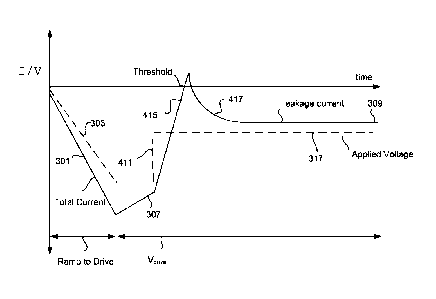
Figure 2 shows a complete current profile and voltage profile for an
electrochromic device employing a simple voltage control algorithm to cause an
optical state transition cycle (tinting followed by clearing) of an
electrochromic
device. In the graph, total current density (I) is represented as a function
of time. As
mentioned, the total current density is a combination of the ionic current
density
associated with an electrochromic transition and electronic leakage current
between
the electrochemically active electrodes. Many different types of electrochomic
devices will have the depicted current profile. In one example, a cathodic
electrochromic material such as tungsten oxide is used in conjunction with an
anodic
electrochromic material such as nickel tungsten oxide in counter electrode. In
such
devices, negative currents indicate coloration/tinting of the device. In one
example,
Date recue/Date received 2023-03-17
lithium ions flow from a nickel tungsten oxide anodically coloring
electrochromic
electrode into a tungsten oxide cathodically coloring electrochromic
electrode.
Correspondingly, electrons flow into the tungsten oxide electrode to
compensate for
the positively charged incoming lithium ions. Therefore, the voltage and
current are
shown to have a negative value.
The depicted profile results from ramping up the voltage to a set level and
then
holding the voltage to maintain the optical state. The current peaks 201 are
associated
with changes in optical state, i.e., tinting and clearing. Specifically, the
current peaks
represent delivery of the ionic charge needed to tint or clear the device.
Mathematically, the shaded area under the peak represents the total charge
required to
tint or clear the device. The portions of the curve after the initial current
spikes
(portions 203) represent electronic leakage current while the device is in the
new
optical state.
In the figure, a voltage profile 205 is superimposed on the current curve. The
voltage profile follows the sequence: negative ramp (207), negative hold
(209),
positive ramp (211), and positive hold (213). Note that the voltage remains
constant
after reaching its maximum magnitude and during the length of time that the
device
remains in its defined optical state. Voltage ramp 207 drives the device to
its new the
tinted state and voltage hold 209 maintains the device in the tinted state
until voltage
ramp 211 in the opposite direction drives the transition from tinted to clear
states. In
some switching algorithms, a current cap is imposed. That is, the current is
not
permitted to exceed a defined level in order to prevent damaging the device
(e.g.
driving ion movement through the material layers too quickly can physically
damage
the material layers). The coloration speed is a function of not only the
applied
voltage, but also the temperature and the voltage ramping rate.
Figure 3 illustrates a voltage control profile in accordance with certain
embodiments. In the depicted embodiment, a voltage control profile is employed
to
drive the transition from a clear state to a tinted state (or to an
intermediate state). To
drive an electrochromic device in the reverse direction, from a tinted state
to a clear
state (or from a more tinted to less tinted state), a similar but inverted
profile is used.
In some embodiments, the voltage control profile for going from tinted to
clear is a
mirror image of the one depicted in Figure 3.
16
Date recue/Date received 2023-03-17
The voltage values depicted in Figure 3 represent the applied voltage (Van))
values. The applied voltage profile is shown by the dashed line. For contrast,
the
current density in the device is shown by the solid line. In the depicted
profile, V npp
includes four components: a ramp to drive component 303, which initiates the
transition, a Vdrive component 313, which continues to drive the transition, a
ramp to
hold component 315, and a Vhoid component 317. Thc ramp components arc
implemented as variations in Van, and the Vdrive and Vhold components provide
constant or substantially constant Vapp magnitudes.
The ramp to drive component is characterized by a ramp rate (increasing
magnitude) and a magnitude of Va,,,e. When the magnitude of the applied
voltage
reaches Vdth,c, the ramp to drive component is completed. The Vdnve component
is
characterized by the value of Vdrivc as well as the duration of Vanvc. The
magnitude of
V drive may be chosen to maintain Veil- with a safe but effective range over
the entire
face of the electrochromic device as described above.
The ramp to hold component is characterized by a voltage ramp rate
(decreasing magnitude) and the value of V hold (or optionally the difference
between
Vdrivo and VI1Old ). V apt) drops according to the ramp rate until the value
of Vhoid is
reached. The \Thou' component is characterized by the magnitude of Vhold and
the
duration of Vhoid. Actually, the duration of Vhoid is typically governed by
the length
of time that the device is held in the tinted state (or conversely in the
clear state).
Unlike the ramp to drive, Vdrive, and ramp to hold components, the Vhde
component
has an arbitrary length, which is independent of the physics of the optical
transition of
the device.
Each type of electrochromic device will have its own characteristic
components of the voltage profile for driving the optical transition. For
example, a
relatively large device and/or one with a more resistive conductive layer will
require a
higher value of Vdn.õ and possibly a higher ramp rate in the ramp to drive
component.
U.S. Patent Application Publication No. 2013/0271814, filed April 17, 2012
discloses
controllers and associated algorithms for driving optical transitions over a
wide range
of conditions. As explained therein, each of the components of an applied
voltage
profile (ramp to drive, Vdrive, ramp to hold, and Vhoid, herein) may be
independently
controlled to address real-time conditions such as
17
Date recue/Date received 2023-03-17
=
current temperature, current level of transmissivity, etc. In some
embodiments, the
values of each component of the applied voltage profile is set for a
particular
electrochromic device (having its own bus bar separation, resistivity, etc.)
and does
not vary based on current conditions. In other words, in such embodiments, the
voltage profile does not take into account feedback such as temperature,
current
density, and the like.
As indicated, all voltage values shown in the voltage transition profile of
Figure 3 correspond to the V app values described above. They do not
correspond to
the Veil' values described above. In other words, the voltage values depicted
in Figure
3 are representative of the voltage difference between the bus bars of
opposite polarity
on the electrochromic device.
In certain embodiments, the ramp to drive component of the voltage profile is
chosen to safely but rapidly induce ionic current to flow between the
electrochromic
and counter electrodes. As shown in Figure 3, the current in the device
follows the
profile of the ramp to drive voltage component until the ramp to drive portion
of the
profile ends and the Vdri, portion begins. See current component 301 in Figure
3.
Safe levels of current and voltage can be determined empirically or based on
other
feedback. U.S. Patent No. 8,254,013, filed March 16, 2011, issued August 28,
2012
presents examples of algorithms for maintaining safe current levels during
electrochromic device transitions.
In certain embodiments, the value of Vdnve is chosen based on the
considerations described above. Particularly, it is chosen so that the value
of Vac over
the entire surface of the electrochromic device remains within a range that
effectively
and safely transitions large electrochromic devices. The duration of Vthive
can be
chosen based on various considerations. One of these ensures that the drive
potential
is held for a period sufficient to cause the substantial coloration of the
device. For this
purpose, the duration of Vdrive may be determined empirically, by monitoring
the
optical density of the device as a function of the length of time that Vdrive
remains in
place. In some embodiments, the duration of Van,. is set to a specified time
period.
In another embodiment, the duration of Vdrive is set to correspond to a
desired amount
of ionic and/or electronic charge being passed. As shown, the current ramps
down
during Vdrivc. See current segment 307.
18
Date recue/Date received 2023-03-17
Another consideration is the reduction in current density in the device as the
ionic current decays as a consequence of the available lithium ions completing
their
journey from the anodic coloring electrode to the cathodic coloring electrode
(or
counter electrode) during the optical transition. When the transition is
complete, the
only current flowing across device is leakage current through the ion
conducting
layer. As a consequence, the ohmic drop in potential across the face of the
device
decreases and the local values of Veff increase. These increased values of
Veff can
damage or degrade the device if the applied voltage is not reduced. Thus,
another
consideration in determining the duration of Vdrive is the goal of reducing
the level of
Veff associated with leakage current. By dropping the applied voltage from
Vdrive to
Vhold, not only is Veff reduced on the face of the device but leakage current
decreases
as well. As shown in Figure 3, the device current transitions in a segment 305
during
the ramp to hold component. The current settles to a stable leakage current
309
during Vhold =
CONTROLLING V DRIVE USING FEEDBACK FROM THE OPTICAL
TRANSITION
A challenge arises because it can be difficult to predict how long the applied
drive voltage should be applied before transitioning to the hold voltage.
Devices of
different sizes, and more particularly devices having bus bars separated by
particular
distances, require different lengths of time for applying the drive voltage.
Further, the
processes employed to fabricate optically switchable devices such as
electrochromic
devices may vary subtly from one batch to another or one process revision to
another.
The subtle process variations translate into potentially different
requirements for the
length of time that the drive voltage must be applied to the devices used in
operation.
Still further, environmental conditions, and particularly temperature, can
influence the
length of time that the applied voltage should be applied to drive the
transition.
To account for all these variables, current technology may define many
distinct control algorithms with distinct periods of time for applying a
defined drive
voltage for each of many different window sizes or device features. A
rationale for
doing this is to ensure that the drive voltage is applied for a sufficient
period,
19
Date recue/Date received 2023-03-17
regardless of device size and type, to ensure that the optical transition is
complete.
Currently many different sized electrochromic windows are manufactured. While
it is
possible to pre-determine the appropriate drive voltage time for each and
every
different type of window, this can be a tedious, expensive, and time-consuming
process. An improved approach, described here, is to determine on-the-fly the
length
of time that the drive voltage should be applied.
Further, it may be desirable to cause the transition between two defined
optical
states to occur within a defined duration, regardless of the size of the
optically
switchable device, the process under which the device is fabricated, and the
environmental conditions in which the device is operating at the time of the
transition.
This goal can be realized by monitoring the course of the transition and
adjusting the
drive voltage as necessary to ensure that the transition completes in the
defined time.
Adjusting the magnitude of the drive voltage is one way of accomplishing this.
Certain disclosed embodiments apply a probing technique to assess the
progress of an optical transition while the device is in transition. As
illustrated in
Figure 3, there are typically distinct ramp to drive and the drive voltage
maintenance
stages of the optical transition. The probe technique can be applied during
either of
these. In many embodiments, it is applied during the drive voltage maintenance
portion of the algorithm.
In certain embodiments, the probing technique involves pulsing the current or
voltage applied to drive the transition and then monitoring the current or
voltage
response to detect an overdrive condition in the vicinity of the bus bars. An
overdrive
condition occurs when the local effective voltage is greater than needed to
cause a
local optical transition. For example, if an optical transition to a clear
state is deemed
complete when Veff reaches 2V, and the local value of Veff near a bus bar is
2.2V, the
position near the bus bar may be characterized as in an overdrive condition.
One example of a probing technique involves pulsing the applied drive voltage
by dropping it to the level of the hold voltage (or the hold voltage modified
by an
appropriate offset) and monitoring the current response to determine the
direction of
the current response. In this example, when the current response reaches a
defined
Date recue/Date received 2023-03-17
threshold, the device control system determines that it is now time to
transition from
the drive voltage to the hold voltage.
Figure 4A is a graph depicting an optical transition in which a drop in
applied
voltage from Vdrive to Vhdd results in a net current flow establishing that
the optical
transition has proceeded far enough to permit the applied voltage to remain at
Vhoid
for the duration of the ending optical state. This is illustrated by a voltage
drop 411 in
V app from VdrivctoVhold. Voltage drop 411 is performed during a period when
the
V app might otherwise be constrained to remain in the drive phase shown in
Figure 3.
The current flowing between the bus bars began dropping (becoming less
negative),
as illustrated by current segment 307, when the applied voltage initially
stopped
increasing (becoming more negative) and plateaued at Vdrive. However, when the
applied voltage now dropped at 411, the current began decreasing more readily
as
illustrated by current segment 415. In accordance with some embodiments, the
level
of current is measured after a defined period of time passes following the
voltage drop
411. If the current is below a certain threshold, the optical transition is
deemed
complete, and the applied voltage may remain at Vhoid (or move to Vhold if it
is at
some other level below Vthive). In the particular example of Figure 4A, the
current
threshold is exceeded as illustrated. Therefore, the Vapp remains at Vhold for
the
duration of the ending optical state. Vhdd may be selected for the ending
optical state
it provides. Such ending optical state may be a maximum, minimum, or
intermediate
optical state for the optical device undergoing the transition.
In situations where the current does not reach the threshold when measured, it
may be appropriate to return Vapp Vthiõ. Figure 4B illustrates this situation.
Figure
4B is a graph depicting an optical transition in which an initial drop in
applied voltage
from Vdrive to Vliold (see 411) results in a net current flow indicating that
the optical
transition has not yet proceeded far enough to permit the applied voltage to
remain at
Vhoid for the duration of the ending optical state. Note that current segment
415,
which has a trajectory resulting from voltage drop 411, does not reach the
threshold
when probed at 419. Therefore the applied voltage is returned to Vdrive for a
further
period of time ¨ while the current recovers at 417 ¨ before again dropping
again to
Vhoid (421) at which point the resulting current (423) establishes that the
optical
transition has proceeded far enough to permit the applied voltage to remain at
Vhoid
21
Date recue/Date received 2023-03-17
for the duration of the ending optical state. As explained, the ending optical
state may
be a maximum, minimum, or intermediate optical state for the optical device
undergoing the transition.
As explained, the hold voltage is a voltage that will maintain the optical
device
in equilibrium at a particular optical density or other optical condition. It
produces a
steady-state result by generating a current that offsets the leakage current
in the
ending optical state. The drive voltage is applied to speed the transition to
a point
where applying the hold voltage will result in a time invariant desired
optical state.
The probing technique described herein may be understood in terms of the
physical mechanisms associated with an optical transition driven from bus bars
at the
edges of a device. Basically, the technique relies on differential values of
the
effective voltage experienced in the optically switchable device across the
face of the
device, and particularly the variation in Veff from the center of the device
to the edge
of the device. The local variation in potential on the transparent conductive
layers
results in different values of Veff across the face of the device. The value
of Veff
experienced by the optically switchable device near the bus bars is far
greater the
value of Veff in the center of the device. As a consequence, the local charge
buildup in
the region next to the bus bars is significantly greater than the charge
buildup in the
center the device.
At some point during the optical transition, the value of Veff at the edge of
the
device near the bus bars is sufficient to exceed the ending optical state
desired for the
optical transition whereas in the center of the device, the value of Veff is
insufficient
to reach that ending state. The ending state may be an optical density value
associated
with the endpoint in the optical transition. While in this intermediate stage
of the
optical transition, if the drive voltage is dropped to the hold voltage, the
portion of the
electrochromic device close to the bus bars will effectively try to transition
back
toward the state from which it started. However, as the device state in the
center of the
device has not yet reached the end state of the optical transition, when a
hold voltage
is applied, the center portion of the device will continue transitioning in
the direction
desired for the optical transition.
22
Date recue/Date received 2023-03-17
When the device in this intermediate stage of transition experiences the
change in applied voltage from the drive voltage to the hold voltage (or some
other
suitably lower magnitude voltage), the portions of the device located near the
bus bars
- where the device is effectively overdriven - generate current flowing in the
direction
opposite that required to drive the transition. In contrast, the regions of
the device in
the center, which have not yet fully transitioned to the final state, continue
to promote
current flow in a direction required to drive the transition.
Over the course of the optical transition, and while the device is
experiencing
the applied drive voltage, there is a gradual increase in the driving force
for causing
current to flow in the reverse direction when the device is subject to a
sudden drop in
applied voltage. By monitoring the flow of current in response to
perturbations away
from drive voltage, one can determine a point at which the transition from the
first
state to the second state is sufficiently far along that a transition from
drive voltage to
hold voltage is appropriate. By "appropriate," it is meant that the optical
transition is
sufficiently complete from the edge of the device to the center of the device.
Such
transition can be defined in many ways depending upon the specifications of
the
product and its application. In one embodiment, it assumes that the transition
from the
first state to the second state is at least about 80% of complete or at least
about 95% of
complete. Complete reflecting the change in optical density from the first
state to the
second state. The desired level of completeness may correspond to a threshold
current level as depicted in the examples of Figures 4A and 4B.
Many possible variations to the probing protocol exist. Such variations may
include certain pulse protocols defined in terms of the length of time from
the
initiation of the transition to the first pulse, the duration of the pulses,
the size of the
pulses, and the frequency of the pulses.
In one embodiment, the pulse sequence is begun immediately upon the
application of a drive voltage or a ramp to drive voltage that initiates the
transition
between the first optical state and second optical state. In other words,
there would be
no lag time between the initiation of the transition and the application of
pulsing. In
some implementations, the probe duration is sufficiently short (e.g., about 1
second or
less) that probing back and forth between Vdrive and Vhoid for the entire
transition is
not significantly detrimental to switching time. However, in some embodiments,
it is
23
Date recue/Date received 2023-03-17
unnecessary to start probing right away. In some cases, switching is initiated
after
about 50% of an expected or nominal switching period is complete, or about 75%
of
such period is complete. Often, the distance between bus bars is known or can
be
read using an appropriately configured controller. With the distance known, a
conservative lower limit for initiating probing may be implemented based on
approximate known switching time. As an example, the controller may be
configured
to initiate probing after about 50-75% of expected switching duration is
complete.
In some embodiments, the probing begins after about 30 seconds from
initiating the optical transition. Relatively earlier probing may be
especially helpful
in cases where an interrupt command is received. An interrupt command is one
that
instructs the device to switch to a third optical transmission state when the
device is
already in the process of changing from a first to a second optical
transmission state).
In this case, early probing can help determine the direction of the transition
(i.e,
whether the interrupt command requires the window to become lighter or darker
than
when the command is received). In some embodiments, the probing begins about
120
minutes (e.g., about 30 minutes, about 60 minutes, or about 90 minutes) after
initiating the optical transition. Relatively later probing may be more useful
where
larger windows are used, and where the transition occurs from an equilibrium
state.
For architectural glass, probing may begin about 30 seconds to 30 minutes
after
initiating the optical transition, in some cases between about 1-5 minutes,
for example
between about 1-3 minutes, or between about 10-30 minutes, or between about 20-
30
minutes. In some embodiments, the probing begins about 1-5 minutes (e.g.,
about 1-3
minutes, about 2 minutes in a particular example) after initiating an optical
transition
through an interrupt command, while the probing begins about 10-30 minutes
(e.g.,
about 20-30 minutes) after initiating an optical transition from an initial
command
given when the electrochromic device is in an equilibrium state.
In the examples of Figures 4A and 4B, the size of the pulses is between the
drive voltage value and the hold voltage value. This may be done for
convenience.
Other pulse magnitudes are possible. For example, the pulse may a magnitude of
about +/- about 500 mV of the hold voltage, or about +/- 200 mV of the hold
voltage.
For context, an electrochromic device on a window, such as an architectural
window,
may have a drive voltage of about 0 volts to +/- 20 volts (e.g., about +/- 2
volts to +/-
24
Date recue/Date received 2023-03-17
volts) and a hold voltage of about 0 volts to +/- 4 volts (e.g., about +/- 1
volt to +/-
2 volts).
In various embodiments, the controller determines when during the optical
transition the polarity of the probe current opposes the polarity of the bias
due to
5 transition proceeding to a significant extent. In other words, the
current to the bus bars
flows in a direction opposite of what would be expected if the optical
transition was
still proceeding.
Probing by dropping the applied voltage magnitude from Vdrive to Vhoid
provides a convenient, and broadly applicable, mechanism for monitoring the
10 transition to deteimine when the probe current first reverses polarity.
Probing by
dropping the voltage to a magnitude other than that of Vhoid may involve
characterization of window performance. It appears that even very large
windows
(e.g., about 60") essentially complete their optical transition when the
current first
opposes the transition upon probing from Varilre to Vhold=
In certain cases, probing occurs by dropping the applied voltage magnitude
from Vdrive toVprobc, where Voroho is a probe voltage other than the hold
voltage. For
example, Vprobc may be Vhoid as modified by an offset. Although many windows
are
able to essentially complete their optical transitions when the current first
opposes the
transition after probing from Vdrive to Vhoid, certain windows may benefit
from pulsing
to a voltage slightly offset from the hold voltage. In general, the offset
becomes
increasingly beneficial as the size of the window increases, and as the
temperature of
the window drops. In certain cases, the offset is between about 0-1V, and the
magnitude of Vp,oh, is between about 0-1V higher than the magnitude of Vhold.
For
example, the offset may be between about 0-0.4V. In these or other
embodiments, the
offset may be at least about 0.025V, or at least about 0.05V, or at least
about 0.1V.
The offset may result in the transition having a longer duration than it
otherwise
would. The longer duration helps ensure that the optical transition is able to
fully
complete. Techniques for selecting an appropriate offset from the hold voltage
are
discussed further below in the context of a target open circuit voltage.
In some embodiments, the controller notifies a user or the window network
master controller of how far (by, e.g., percentage) the optical transition has
Date recue/Date received 2023-03-17
progressed. This may be an indication of what transmission level the center of
the
window is currently at. Feedback regarding transition may be provided to user
interface in a mobile device or other computational apparatus. See e.g., PCT
Patent
Application No. 1JS2013/036456 filed April 12,2013.
The frequency of the probe pulsing may be between about 10 seconds and 500
seconds. As used in this context, the "frequency" means the separation time
between
the midpoints of adjacent pulses in a sequence of two or more pulses.
Typically, the
frequency of the pulsing is between about 10 seconds and 120 seconds. In
certain
embodiments, the frequency the pulsing is between about 20 seconds and 30
seconds.
In certain embodiments, the probe frequency is influenced by the size of the
electrochromic device or the separation between bus bars in the device. In
certain
embodiments, the probe frequency is chosen as a function the expected duration
of the
optical transition. For example, the frequency may be set to be about 115th to
about
11.501h (or about 1/1 0th to about 1/30'1) of the expected duration of the
transition time.
Note that transition time may correspond to the expected duration of Van,
\IMAM.
Note also that the expected duration of the transition may be a function of
the size of
the electrochromic device (or separation of bus bars). In one example, the
duration
for 14" windows is ¨2.5 minutes, while the duration for 60" windows is ¨40
minutes.
In one example, the probe frequency is every 6.5 seconds for a 14" window and
every
2 minutes for a 60" window.
In various implementations, the duration of each pulse is between about 1x10⁻⁵
and 20 seconds. In some embodiments, the duration of the pulses is between
about 0.1
and 20 seconds, for example between about 0.5 seconds and 5 seconds.
As indicated, in certain embodiments, an advantage of the probing techniques
disclosed herein is that only very little information need be pre-set with the
controller
that is responsible for controlling a window transition. Typically, such
information
includes only the hold voltage (and voltage offset, if applicable) associated
for each
optical end state. Additionally, the controller may specify a difference in
voltage
between the hold voltage and a drive voltage, or alternatively, the value of
Varive
itself. Therefore, for any chosen ending optical state, the controller would
know the
magnitudes of V hold. Varso and Vdrive. The duration of the drive voltage is
determined
26
Date recue/Date received 2023-03-17
using the probing algorithm described here. In other words, the controller
determines
how to appropriately apply the drive voltage as a consequence of actively
probing the
extent of the transition in real time.
Figure 5A presents a flowchart 501 for a process of monitoring and controlling
an optical transition in accordance with certain disclosed embodiments. As
depicted,
the process begins with an operation denoted by reference number 503, where a
controller or other control logic receives instructions to direct the optical
transition.
As explained, the optical transition may be an optical transition between a
tinted state
and a more clear state of electrochromic device. The instructions for
directing the
optical transition may be provided to the controller based upon a
preprogrammed
schedule, an algorithm reacting to external conditions, manual input from a
user, etc.
Regardless of how the instructions originate, the controller acts on them by
applying a
drive voltage to the bus bars of the optically switchable device. See the
operation
denoted by reference number 505.
As explained above, in conventional embodiments, the drive voltage is applied
to the bus bars for a defined period of time after which it is presumed that
the optical
transition is sufficiently complete that the applied voltage can be dropped to
a hold
voltage. In such embodiments, the hold voltage is then maintained for the
duration of
the pending optical state. In contrast, in accordance with embodiments
disclosed
herein, the transition from a starting optical state to an ending optical
state is
controlled by probing the condition of the optically switchable device one or
more
times during the transition. This procedure is reflected in operations 507, et
seq. of
Figure 5A.
In operation 507, the magnitude of the applied voltage is dropped after
allowing the optical transition to proceed for an incremental period of time.
The
duration of this incremental transition is significantly less than the total
duration
required to fully complete the optical transition. Upon dropping the magnitude
of the
applied voltage, the controller measures the response of the current flowing
to the bus
bars. See operation 509. The relevant controller logic may then determine
whether the
current response indicates that the optical transition is nearly complete. See
decision
511. As explained above, the determination of whether an optical transition is
nearly
complete can be accomplished in various ways. For example, it may be
determined by
27
Date recue/Date received 2023-03-17
the current reaching a particular threshold. Assuming that the current
response does
not indicate that the optical transition is nearly complete, process control
is directed to
an operation denoted by reference number 513. In this operation, the applied
voltage
is returned to the magnitude of the drive voltage. Process controls then loops
back to
operation 507 where the optical transition is allowed to proceed by a further
increment before again dropping the magnitude of the applied voltage to the
bus bars.
At some point in the procedure 501, decision operation 511 determines that
the current response indicates that the optical transition is in fact nearly
complete. At
this point, process control proceeds to an operation indicated by reference
number
515, where the applied voltage is transitioned to or maintained at the hold
voltage for
the duration of the ending optical state. At this point, the process is
complete.
Separately, in some implementations, the method or controller may specify a
total duration of the transition. In such implementations, the controller may
be
programmed to use a modified probing algorithm to monitor the progress of the
transition from the starting state to the end state. The progress can be
monitored by
periodically reading a current value in response to a drop in the applied
voltage
magnitude such as with the probing technique described above. The probing
technique may also be implemented using a drop in applied current (e.g.,
measuring
the open circuit voltage) as explained below. The current or voltage response
indicates how close to completion the optical transition has come. In some
cases, the
response is compared to a threshold current or voltage for a particular time
(e.g., the
time that has elapsed since the optical transition was initiated). In some
embodiments,
the comparison is made for a progression of the current or voltage responses
using
sequential pulses or checks. The steepness of the progression may indicate
when the
end state is likely to be reached. A linear extension to this threshold
current may be
used to predict when the transition will be complete, or more precisely when
it will be
sufficiently complete that it is appropriate to drop the drive voltage to the
hold
voltage.
With regard to algorithms for ensuring that the optical transition from first
state to the second state occurs within a defined timeframe, the controller
may be
configured or designed to increase the drive voltage as appropriate to speed
up the
transition when the interpretation of the pulse responses suggests that the
transition is
28
Date recue/Date received 2023-03-17
not progressing fast enough to meet the desired speed of transition. In
certain
embodiments, when it is determined that the transition is not progressing
sufficiently
fast, the transition switches to a mode where it is driven by an applied
current. The
current is sufficiently great to increase the speed of the transition but is
not so great
that it degrades or damages the electrochromic device. In some
implementations, the
maximum suitably safe current may be referred to as ',are. Examples of 55f may
range
between about 5 and 2501.1A/cm2. In current controlled drive mode, the applied
voltage is allowed to float during the optical transition. Then, during this
current
controlled drive step, could the controller periodically probes by, e.g.,
dropping to the
hold voltage and checking for completeness of transition in the same way as
when
using a constant drive voltage.
In general, the probing technique may determine whether the optical transition
is progressing as expected. If the technique determines that the optical
transition is
proceeding too slowly, it can take steps to speed the transition. For example,
it can
increase the drive voltage. Similarly, the technique may determine that the
optical
transition is proceeding too quickly and risks damaging the device. When such
determination is made, the probing technique may take steps to slow the
transition.
As an example, the controller may reduce the drive voltage.
In some applications, groups of windows are set to matching transition rates
by adjusting the voltage and/or driving current based on the feedback obtained
during
the probing (by pulse or open circuit measurements). In embodiments where the
transition is controlled by monitoring the current response, the magnitude of
the
current response may be compared from controller to controller (for each of
the group
of windows) to determine how to scale the driving potential or driving current
for
each window in the group. The rate of change of open circuit voltage could be
used in
the same manner.
Figure 5B presents a flowchart 521 depicting an example process for ensuring
that the optical transition occurs sufficiently fast, e.g., within a defined
time period.
The first four depicted operations in flowchart 521 correspond to the first
four
operations in flowchart 501. In other words, operation 523, 525, 527, and 529
of
flowchart 521 correspond to operations 503, 505, 507, and 509 of flowchart
501.
Briefly, in operation 523, the controller or other appropriate logic receives
29
Date recue/Date received 2023-03-17
instructions to undergo an optical transition. Then, at operation 525, the
controller
applies a drive voltage to the bus bars. After allowing the optical transition
to proceed
incrementally, the controller drops the magnitude of the applied voltage to
the bus
bars. See operation 527. The magnitude of the lower voltage is typically,
though not
necessarily, the hold voltage. As mentioned, the lower voltage may also be the
hold
voltage as modified by an offset (the offset often falling between about 0-1V,
for
example between about 0-0.4V in many cases). Next, the controller measures the
current response to the applied voltage drop. See operation 529.
The controller next determines whether the current response indicates that the
optical transition is proceeding too slowly. See decision 531. As explained,
the
current response may be analyzed in various ways determine whether the
transition is
proceeding with sufficient speed. For example, the magnitude of the current
response
may be considered or the progression of multiple current responses to multiple
voltage pulses may be analyzed to make this determination.
Assuming that operation 531 establishes that the optical transition is
proceeding rapidly enough, the controller then increases the applied voltage
back to
the drive voltage. See operation 533. Thereafter, the controller then
determines
whether the optical transition is sufficiently complete that further progress
checks are
unnecessary. See operation 535. In certain embodiments, the determination in
operation 535 is made by considering the magnitude of the current response as
discussed in the context of Figure 5A. Assuming that the optical transition is
not yet
sufficiently complete, process control returns to operation 527, where the
controller
allows the optical transition to progress incrementally further before again
dropping
the magnitude of the applied voltage.
Assuming that execution of operation 531 indicates that the optical transition
is proceeding too slowly, process control is directed to an operation 537
where the
controller increases the magnitude of the applied voltage to a level that is
greater than
the drive voltage. This over drives the transition and hopefully speeds it
along to a
level that meets specifications. After increasing the applied voltage to this
level,
process control is directed to operation 527 where the optical transition
continues for
a further increment before the magnitude of the applied voltage is dropped.
The
overall process then continues through operation 529, 531, etc. as described
above. At
Date recue/Date received 2023-03-17
some point, decision 535 is answered in the affii ____________________ !native
and the process is complete.
In other words, no further progress checks are required. The optical
transition then
completes as illustrated in, for example, flowchart 501.
Another application of the probing techniques disclosed herein involves on-
the-fly modification of the optical transition to a different end state. In
some cases, it
will be necessary to change the end state after a transition begins. Examples
of
reasons for such modification include a user's manual override a previously
specified
end tint state and a wide spread electrical power shortage or disruption. In
such
situations, the initially set end state might be transmissivity = 40% and the
modified
end state might be transmissivity = 5%.
Where an end state modification occurs during an optical transition, the
probing techniques disclosed herein can adapt and move directly to the new end
state,
rather than first completing the transition to the initial end state.
In some implementations, the transition controller/method detects the current
state of the window using a voltage/current sense as disclosed herein and then
moves
to a new drive voltage immediately. The new drive voltage may be determined
based
on the new end state and optionally the time allotted to complete the
transition. If
necessary, the drive voltage is increased significantly to speed the
transition or drive a
greater transition in optical state. The appropriate modification is
accomplished
without waiting for the initially defined transition to complete. The probing
techniques disclosed herein provide a way to detect where in the transition
the device
is and make adjustments from there.
It should be understood that the probing techniques presented herein need not
be limited to measuring the magnitude of the device's current in response to a
voltage
drop (pulse). There are various alternatives to measuring the magnitude of the
current
response to a voltage pulse as an indicator of how far as the optical
transition has
progressed. In one example, the profile of a current transient provides useful
information. In another example, measuring the open circuit voltage of the
device
may provide the requisite information. In such embodiments, the pulse involves
simply applying no voltage to device and then measuring the voltage that the
open
circuit device applies. Further, it should be understood that current and
voltage based
31
Date recue/Date received 2023-03-17
algorithms are equivalent. In a current based algorithm, the probe is
implemented by
dropping the applied current and monitoring the device response. The response
may
be a measured change in voltage. For example, the device may be held in an
open
circuit condition to measure the voltage between bus bars.
Figure 5C presents a flowchart 501 for a process of monitoring and controlling
an optical transition in accordance with certain disclosed embodiments. In
this case,
the process condition probed is the open circuit voltage, as described in the
previous
paragraph. The first two depicted operations in flowchart 541 correspond to
the first
two operations in flowcharts 501 and 521. In other words, operations 543 and
545 of
flowchart 541 correspond to operations 503 and 505 of flowchart 501. Briefly,
in
operation 543, the controller or other appropriate logic receives instructions
to
undergo an optical transition. Then, at operation 545, the controller applies
a drive
voltage to the bus bars. After allowing the optical transition to proceed
incrementally,
the controller applies open circuit conditions to the electrochromic device at
operation
547. Next, the controller measures the open circuit voltage response at
operation 549.
As is the case above, the controller may measure the electronic response (in
this case the open circuit voltage) after a defined period has passed since
applying the
open circuit conditions. Upon application of open circuit conditions, the
voltage
typically experiences an initial drop relating to the ohmic losses in external
components connected to the electrochromic device. Such external components
may
be, for example, conductors and connections to the device. After this initial
drop, the
voltage experiences a first relaxation and settles at a first plateau voltage.
The first
relaxation relates to internal ohmic losses, for example over the
electrode/electrolyte
interfaces within the electrochromic devices. The voltage at the first plateau
corresponds to the voltage of the cell, with both the equilibrium voltage and
the
overvoltages of each electrode. After the first voltage plateau, the voltage
experiences
a second relaxation to an equilibrium voltage. This second relaxation is much
slower,
for example on the order of hours. In some cases it is desirable to measure
the open
circuit voltage during the first plateau, when the voltage is relatively
constant for a
short period of time. This technique may be beneficial in providing especially
reliable
open circuit voltage readings. In other cases, the open circuit voltage is
measured at
some point during the second relaxation. This technique may be beneficial in
32
Date recue/Date received 2023-03-17
providing sufficiently reliable open circuit readings while using less
expensive and
quick-operating power/control equipment.
In some embodiments, the open circuit voltage is measured after a set period
of time after the open circuit conditions are applied. The optimal time period
for
measuring the open circuit voltage is dependent upon the distance between the
bus
bars. The set period of time may relate to a time at which the voltage of a
typical or
particular device is within the first plateau region described above. In such
embodiments, the set period of time may be on the order of milliseconds (e.g.,
a few
milliseconds in some examples). In other cases, the set period of time may
relate to a
time at which the voltage of a typical or particular device is experiencing
the second
relaxation described above. Here, the set period of time may be on the order
of about
1 second to several seconds, in some cases. Shorter times may also be used
depending on the available power supply and controller. As noted above, the
longer
times (e.g., where the open circuit voltage is measured during the second
relaxation)
may be beneficial in that they still provide useful open circuit voltage
information
without the need for high end equipment capable of operating precisely at very
short
timefiumes.
In certain implementations, the open circuit voltage is measured/recorded
after
a timeframe that is dependent upon the behavior of the open circuit voltage.
In other
words, the open circuit voltage may be measured over time after open circuit
conditions are applied, and the voltage chosen for analysis may be selected
based on
the voltage vs. time behavior. As described above, after application of open
circuit
conditions, the voltage goes through an initial drop, followed by a first
relaxation, a
first plateau, and a second relaxation. Each of these periods may be
identified on a
voltage vs. time plot based on the slope of curve. For example, the first
plateau
region will relate to a portion of the plot where the magnitude of dVoc/dt is
relatively
low. This may correspond to conditions in which the ionic current has stopped
(or
nearly stopped) decaying. As such, in certain embodiments, the open circuit
voltage
used in the feedback/analysis is the voltage measured at a time when the
magnitude of
dVoc/dt drops below a certain threshold.
Returning to Figure 5C, after the open circuit voltage response is measured,
it
can be compared to a target open circuit voltage at operation 551. The target
open
33
Date recue/Date received 2023-03-17
circuit voltage may correspond to the hold voltage. In certain cases,
discussed further
below, the target open circuit voltage corresponds to the hold voltage as
modified by
an offset. Techniques for choosing an appropriate offset from the hold voltage
are
discussed further below. Where the open circuit voltage response indicates
that the
optical transition is not yet nearly complete (i.e., where the open circuit
voltage has
not yet reached the target open circuit voltage), the method continues at
operation
553, where the applied voltage is increased to the drive voltage for an
additional
period of time. After the additional period of time has elapsed, the method
can repeat
from operation 547, where the open circuit conditions are again applied to the
device.
At some point in the method 541, it will be determined in operation 551 that
the open
circuit voltage response indicates that the optical transition is nearly
complete (i.e.,
where the open circuit voltage response has reached the target open circuit
voltage).
When this is the case, the method continues at operation 555, where the
applied
voltage is maintained at the hold voltage for the duration of the ending
optical state.
The method 541 of Figure 5C is very similar to the method 501 of Figure 5A.
The main difference is that in Figure 5C, the relevant variable measured is
the open
circuit voltage, while in Figure 5A, the relevant variable measured is the
current
response when a reduced voltage is applied. In another embodiment, the method
521
of Figure 5B is modified in the same way. In other words, the method 521 may
be
altered such that probing occurs by placing the device in open circuit
conditions and
measuring the open circuit voltage rather than a current response.
In another embodiment, the process for monitoring and controlling an optical
transition takes into account the total amount of charge delivered to the
electrochromic device during the transition, per unit area of the device. This
quantity
may be referred to as the delivered charge density or total delivered charge
density.
As such, an additional criterion such as the total charge density delivered
may be used
to ensure that the device fully transitions under all conditions.
The total delivered charge density may be compared to a threshold charge
density (also referred to as a target charge density) to determine whether the
optical
transition is nearly complete. The threshold charge density may be chosen
based on
the minimum charge density required to fully complete or nearly complete the
optical
transition under the likely operating conditions. In various cases, the
threshold charge
34
Date recue/Date received 2023-03-17
density may be chosen/estimated based on the charge density required to fully
complete or nearly complete the optical transition at a defined temperature
(e.g., at
about -40 C, at about -30 C, at about -20 C, at about -10 C, at about 0 C, at
about
C, at about 20 C, at about 25 C, at about 30 C, at about 40 C, at about 60 C,
etc.).
5 The optimum threshold charge density may also be affected by the
leakage
current of the electrochromic device. Devices that have higher leakage
currents
should have higher threshold charge densities. In some embodiments, an
appropriate
threshold charge density may be determined empirically for an individual
window or
window design. In other cases, an appropriate threshold may be
calculated/selected
10 based on the characteristics of the window such as the size, bus bar
separation
distance, leakage current, starting and ending optical states, etc. Example
threshold
charge densities range between about 1x10⁻⁵ C/cm2 and about 5 C/cm2, for
example
between about 1x10⁴ and about 0.5 C/cm2, or between about 0.005-0.05 C/cm2, or
between about 0.01-0.04 C/cm2, or between about 0.01-0.02 in many cases.
Smaller
threshold charge densities may be used for partial transitions (e.g., fully
clear to 25%
tinted) and larger threshold charge densities may be used for full
transitions. A first
threshold charge density may be used for bleaching/clearing transitions, and a
second
threshold charge density may be used for coloring/tinting transitions. In
certain
embodiments, the threshold charge density is higher for tinting transitions
than for
clearing transitions. In a particular example, the threshold charge density
for tinting is
between about 0.013-0.017 C/cm2, and the threshold charge density for clearing
is
between about 0.016-0.020 C/cm2. Additional threshold charge densities may be
appropriate where the window is capable of transitioning between more than two
states, For instance, if the device switches between four different optical
states: A, B,
C, and D, a different threshold charge density may be used for each transition
(e.g., A
to B, A to C, A to D, B to A, etc.).
In some embodiments, the threshold charge density is determined empirically.
For instance, the amount of charge required to accomplish a particular
transition
between desired end states may be characterized for devices of different
sizes. A
curve may be fit for each transition to correlate the bus bar separation
distance with
the required charge density. Such information may be used to determine the
minimum threshold charge density required for a particular transition on a
given
Date recue/Date received 2023-03-17
window. In some cases, the information gathered in such empirical
determinations is
used to calculate an amount of charge density that corresponds to a certain
level of
change (increase or decrease) in optical density.
Figure 5D presents a flow chart for a method 561 for monitoring and
controlling an optical transition in an electrochromic device. The method
starts at
operations 563 and 565, which correspond to operations 503 and 505 of FIG. 5A.
At
563, the controller or other appropriate logic receives instructions to
undergo an
optical transition. Then, at operation 565, the controller applies a drive
voltage to the
bus bars. After allowing the optical transition to proceed incrementally, the
magnitude of the voltage applied to the bus bars is reduced to a probe voltage
(which
in some cases is the hold voltage, and in other cases is the hold voltage
modified by
an offset) at operation 567. Next at operation 569, the current response to
the reduced
applied voltage is measured.
Thus far, the method 561 of Figure 5D is identical to the method 501 of Figure
5A. However, the two methods diverge at this point in the process, with method
561
continuing at operation 570, where the total delivered charge density is
determined.
The total delivered charge density may be calculated based on the current
delivered to
the device during the optical transition, integrated overtime. At operation
571, the
relevant controller logic may determine whether the current response and total
delivered charge density each indicate that the optical transition is nearly
complete.
As explained above, the determination of whether an optical transition is
nearly
complete can be accomplished in various ways. For example, it may be
determined by
the current reaching a particular threshold, and by the delivered charge
density
reaching a particular threshold. Both the current response and the total
delivered
charge density must indicate that the transition is nearly complete before the
method
can continue on at operation 575, where the applied voltage is transitioned to
or
maintained at the hold voltage for the duration of the ending optical state.
Assuming
at least one of the current response and total delivered charge density
indicate that the
optical transition is not yet nearly complete at operation 571, process
control is
directed to an operation denoted by reference number 573. In this operation,
the
applied voltage is returned to the magnitude of the drive voltage. Process
control then
loops back to operation 567 where the optical transition is allowed to proceed
by a
36
Date recue/Date received 2023-03-17
further increment before again dropping the magnitude of the applied voltage
to the
bus bars.
Figure 5E presents an alternative method for monitoring and controlling an
optical transition in an electrochromic device. The method starts at
operations 583
and 585, which correspond to operations 503 and 505 of FIG. 5A. At 583, the
controller or other appropriate logic receives instructions to undergo an
optical
transition. Then, at operation 585, the controller applies a drive voltage to
the bus
bars. After allowing the optical transition to proceed incrementally, open
circuit
conditions are applied to the device at operation 587. Next at operation 589,
the open
circuit voltage of the device is measured.
Thus far, the method 581 of Figure 5E is identical to the method 541 of Figure
5C. However, the two methods diverge at this point in the process, with method
581
continuing at operation 590, where the total delivered charge density is
determined.
The total delivered charge density may be calculated based on the current
delivered to
the device during the optical transition, integrated over time. At operation
591, the
relevant controller logic may determine whether the open circuit voltage and
total
delivered charge density each indicate that the optical transition is nearly
complete.
Both the open circuit voltage response and the total delivered charge density
must
indicate that the transition is nearly complete before the method can continue
on at
operation 595, where the applied voltage is transitioned to or maintained at
the hold
voltage for the duration of the ending optical state. Assuming at least one of
the open
circuit voltage response and total delivered charge density indicate that the
optical
transition is not yet nearly complete at operation 591, process control is
directed to an
operation denoted by reference number 593. In this operation, the applied
voltage is
returned to the magnitude of the drive voltage. Process control then loops
back to
operation 587 where the optical transition is allowed to proceed by a further
increment before again applying open circuit conditions to the device. The
method
581 of Figure 5E is very similar to the method 561 of Figure 5D. The principal
difference between the two embodiments is that in Figure 5D, the applied
voltage
drops and a current response is measured, whereas in Figure 5E, open circuit
conditions are applied and an open circuit voltage is measured.
37
Date recue/Date received 2023-03-17
Figure 5F illustrates a flowchart for a related method 508 for controlling an
optical transition in an electrochromic device. The method 508 of Figure 5F is
similar
to the method 581 of Figure 5E. The method 508 begins at operation 510 where
the
controller is turned on. Next, at operation 512, the open circuit voltage
(Voc) is read
and the device waits for an initial command. An initial command is received at
operation 514, the command indicating that the window should switch to a
different
optical state. After the command is received, open circuit conditions are
applied and
the open circuit voltage is measured at operation 516. The amount of charge
delivered (Q) may also be read at block 516. These parameters determine the
direction of the transition (whether the window is supposed to get more tinted
or more
clear), and impact the optimal drive parameter. An appropriate drive parameter
(e.g.,
drive voltage) is selected at operation 516. This operation may also involve
revising
the target charge count and target open circuit voltage, particularly in cases
where an
interrupt command is received, as discussed further below.
After the open circuit voltage is read at operation 516, the electrochromic
device is driven for a period of time. The drive duration may be based on the
busbar
separation distance in some cases. In other cases, a fixed drive duration may
be used,
for example about 30 seconds. This driving operation may involve applying a
drive
voltage or current to the device. Operation 518 may also involve modifying a
drive
parameter based on the sensed open circuit voltage and/or charge count. Next,
at
operation 520, it is determined whether the total time of the transition (thus
far) is less
than a threshold time. The threshold time indicated in Figure 5F is 2 hours,
though
other time periods may be used as appropriate. If it is determined that the
total time
of transition is not less than the threshold time (e.g., where the transition
has taken at
least 2 hours and is not yet complete), the controller may indicate that it is
in a fault
state at operation 530. This may indicate that something has caused an error
in the
transition process. Otherwise, where the total time of transition is
determined to be
less than the threshold time, the method continues at operation 522. Here,
open
circuit conditions are again applied, and the open circuit voltage is
measured. At
operation 524, it is determined whether the measured open circuit voltage is
greater
than or equal to the target voltage (in terms of magnitude). If so, the method
continues at operation 526, where it is determined whether the charge count
(Q) is
greater than or equal to the target charge count. If the answer in either of
operations
38
Date recue/Date received 2023-03-17
524 or 526 is no, the method returns to block 518 where the electrochromic
device
transition is driven for an additional drive duration. Where the answer in
both of
operations 524 and 526 is yes, the method continues at operation 528, where a
hold
voltage is applied to maintain the electrochromie device in the desired tint
state.
Typically, the hold voltage continues to be applied until a new command is
received,
or until a timeout is experienced.
When a new command is received after the transition is complete, the method
may return to operation 516. Another event that can cause the method to return
to
operation 516 is receiving an interrupt command, as indicated in operation
532. An
interrupt command may be received at any point in the method after an initial
command is received at operation 514 and before the transition is essentially
complete
at operation 528. The controller should be capable of receiving multiple
interrupt
commands over a transition. One example interrupt command involves a user
directing a window to change from a first tint state (e.g., fully clear) to a
second tint
state (e.g., fully tinted), then interrupting the transition before the second
tint state is
reached to direct the window to change to a third tint state (e.g., half
tinted) instead of
the second tint state. After receiving a new command or an interrupt command,
the
method returns to block 516 as indicated above. Here, open circuit conditions
are
applied and the open circuit voltage and charge count are read. Based on the
open
circuit voltage and charge count readings, as well as the desired third/final
tint state,
the controller is able to determine appropriate drive conditions (e.g., drive
voltage,
target voltage, target charge count, etc.) for reaching the third tint state.
For instance,
the open circuit voltage/charge count may be used to indicate in which
direction the
transition should occur. The charge count and charge target may also be reset
after
receiving a new command or an interrupt command. The updated charge count may
relate to the charge delivered to move from the tint state when the
new/interrupt
command is received to the desired third tint state. Because the new
command/interrupt command will change the starting and ending points of the
transition, the target open circuit voltage and target charge count may need
to be
revised. This is indicated as an optional part of operation 516, and is
particularly
relevant where a new or interrupt command is received.
39
Date recue/Date received 2023-03-17
In certain implementations, the method involves using a static offset to the
hold voltage. This offset hold voltage may be used to probe the device and
elicit a
current response, as described in relation to Figures 5A, 5B, and 5D. The
offset hold
voltage may also be used as a target open circuit voltage, as described in
relation to
Figure 5C and 5E. In certain cases, particularly for windows with a large
separation
between the bus bars (e.g., at least about 25"), the offset can be beneficial
in ensuring
that the optical transition proceeds to completion across the entire window.
In many cases, an appropriate offset is between about 0-0.5V (e.g., about 0.1-
0.4V, or between about 0.1-0.2V). Typically, the magnitude of an appropriate
offset
increases with the size of the window. An offset of about 0.2V may be
appropriate
for a window of about 14 inches, and an offset of about 0.4V may be
appropriate for a
window of about 60 inches. These values are merely examples and are not
intended
to be limiting. In some embodiments, a window controller is programmed to use
a
static offset to VhoId. The magnitude and in some cases direction of the
static offset
may be based on the device characteristics such as the size of the device and
the
distance between the bus bars, the driving voltage used for a particular
transition, the
leakage current of the device, the peak current density, capacitance of the
device, etc.
In various embodiments, the static offset is determined empirically. In some
designs,
it is calculated dynamically, when the device is installed or while it is
installed and
operating, from monitored electrical and/or optical parameters or other
feedback.
In other embodiments, a window controller may be programmed to
dynamically calculate the offset to Vhold= In one implementation, the window
controller dynamically calculates the offset to Vhdd based on one or more of
the
device's current optical state (OD), the current delivered to the device (I),
the rate of
change of current delivered to the device (dI/dt), the open circuit voltage of
the device
(V), and the rate of change of the open circuit voltage of the device
(dVoc/dt). This
embodiment is particularly useful because it does not require any additional
sensors
for controlling the transition. Instead, all of the feedback is generated by
pulsing the
electronic conditions and measuring the electronic response of the device. The
feedback, along with the device characteristics mentioned above, may be used
to
calculate the optimal offset for the particular transition occurring at that
time. In other
embodiments, the window controller may dynamically calculate the offset to
Vhold
Date recue/Date received 2023-03-17
based on certain additional parameters. These additional parameters may
include the
temperature of the device, ambient temperature, and signals gathered by
photoptic
sensors on the window. These additional parameters may be helpful in achieving
uniform optical transitions at different conditions. However, use of these
additional
parameters also increases the cost of manufacture due to the additional
sensors
required.
The offset may be beneficial in various cases due to the non-uniform quality
of the effective voltage, Veff, applied across the device. The non-uniform
Veff is
shown in Figure 2, for example, described above. Because of this non-
uniformity, the
optical transition does not occur in a uniform manner. In particular, areas
near the bus
bars experience the greatest Val, and transition quickly, while areas removed
from the
bus bars (e.g., the center of the window) experience the lowest V eff and
transition
more slowly. The offset can help ensure that the optical transition proceeds
to
completion at the center of the device where the change is slowest.
Figures 6A and 6B show graphs depicting the total charge delivered over time
and the applied voltage over time during two different electrochromic tinting
transitions. The window in each case measured about 24x24 inches. The total
charge
delivered is referred to as the Tint Charge Count, and is measured in coulombs
(C).
The total charge delivered is presented on the left hand y-axis of each graph,
and the
applied voltage is presented on the right hand y-axis of each graph. In each
figure,
line 602 corresponds to the total charge delivered and line 604 corresponds to
the
applied voltage. Further, line 606 in each graph corresponds to a threshold
charge
(the threshold charge density multiplied by the area of the window), and line
608
corresponds to a target open circuit voltage. The threshold charge and target
open
circuit voltage are used in the method shown in Figure 5E to monitor/control
the
optical transition.
The voltage curves 604 in Figures 6A and 6B each start out with a ramp to
drive component, where the magnitude of the voltage ramps up to the drive
voltage of
about -2.5V. After an initial period of applying the drive voltage, the
voltage begins
to spike upwards at regular intervals. These voltage spikes occur when the
electrochromic device is being probed. As described in Figure 5E, the probing
occurs
by applying open circuit conditions to the device. The open circuit conditions
result
41
Date recue/Date received 2023-03-17
in an open circuit voltage, which correspond to the voltage spikes seen in the
graphs.
Between each probe/open circuit voltage, there is an additional period where
the
applied voltage is the drive voltage. In other words, the electrochromic
device is
driving the transition and periodically probing the device to test the open
circuit
voltage and thereby monitor the transition. The target open circuit voltage,
represented by line 608, was selected to be about -1.4V for each case. The
hold
voltage in each case was about -1.2V. Thus, the target open circuit voltage
was offset
from the hold voltage by about 0.2V.
In the transition of Figure 6A, the magnitude of the open circuit voltage
exceeds the magnitude of the target open circuit voltage at about 1500
seconds.
Because the relevant voltages in this example are negative, this is shown in
the graph
as the point at which the open circuit voltage spikes first fall below the
target open
circuit voltage. In the transition of Figure 6B, the magnitude of the open
circuit
voltage exceeds the magnitude of the target open circuit voltage sooner than
in Figure
6A, around 1250 seconds.
The total delivered charge count curves 602 in Figures 6A and 6B each start at
0 and rise monotonically. In the transition of Figure 6A, the delivered charge
reaches
the threshold charge at around 1500 seconds, which was very close to the time
at
which the target open circuit voltage was met. Once both conditions were met,
the
voltage switched from the drive voltage to the hold voltage, around 1500
seconds. In
the transition of Figure 6B, the total delivered charge took about 2100
seconds to
reach the charge threshold, which is about 14 minutes longer than it took the
voltage
to reach the target voltage for this transition. After both the target voltage
and
threshold charge are met, the voltage is switched to the hold voltage. The
additional
requirement of the total charge delivered results in the FIG. 6B case driving
the
transition at the drive voltage for a longer time than might otherwise be
used. This
helps ensure full and uniform transitions across many window designs at
various
environmental conditions.
In another embodiment, the optical transition is monitored through voltage
sensing pads positioned directly on the transparent conductive layers (TCLs).
This
allows for a direct measurement of the V eff at the center of the device,
between the
bus bars where V eff is at a minimum. In this case, the controller indicates
that the
42
Date recue/Date received 2023-03-17
optical transition is complete when the measured Veff at the center of the
device
reaches a target voltage such as the hold voltage. In various embodiments, the
use of
sensors may reduce or eliminate the benefit from using a target voltage that
is offset
from the hold voltage. In other words, the offset may not be needed and the
target
voltage may equal the hold voltage when the sensors are present. Where voltage
sensors are used, there should be at least one sensor on each TCL. The voltage
sensors may be placed at a distance mid-way between the bus bars, typically
off to a
side of the device (near an edge) so that they do not affect (or minimally
affect) the
viewing area. The voltage sensors may be hidden from view in some cases by
placing
them proximate a spacer/separator and/or frame that obscures the view of the
sensor.
Figure 6C presents an embodiment of an EC window 690 that utilizes sensors
to directly measure the effective voltage at the center of the device. The EC
window
690 includes top bus bar 691 and bottom bus bar 692, which are connected by
wires
693 to a controller (not shown). Voltage sensor 696 is placed on the top TCL,
and
voltage sensor 697 is placed on the bottom TCL. The sensors 696 and 697 are
placed
at a distance mid-way between the bus bars 691 and 692, though they are off to
the
side of the device. In some cases the voltage sensors may be positioned such
that they
reside within a frame of the window. This placement helps hide the sensors and
promote optimal viewing conditions. The voltage sensors 696 and 697 are
connected
to the controller through wires 698. The wires 693 and 698 may pass under or
through a spacer/separator placed and sealed in between the panes of the
window.
The window 690 shown in Figure 6C may utilize any of the methods described
herein
for controlling an optical transition.
In some implementations, the voltage sensing pads may be conductive tape
pads. The pads may be as small as about 1 mm2 in some embodiments. In these or
other cases, the pads may be about 10 mm2 or less. A four wire system may be
used
in embodiments utilizing such voltage sensing pads.
ELECTROCHROMIC DEVICES AND CONTROLLERS ¨ EXAMPLES
Examples of electrochromic device structure and fabrication will now be
presented. Figures 7A and 7B are schematic cross-sections of an electrochromic
device, 700, showing a common structural motif for such devices.
Electrochromic
43
Date recue/Date received 2023-03-17
device 700 includes a substrate 702, a conductive layer (CL) 704, an
electrochromic
layer (EC) 706, an optional ion conducting (electronically resistive) layer
(IC) 708, a
counter electrode layer (CE) 710, and another conductive layer (CL) 712.
Elements
704, 706, 708, 710, and 712 are collectively referred to as an electrochromic
stack,
714. In numerous embodiments, the stack does not contain ion conducting layer
708,
or at least not as a discrete or separately fabricated layer. A voltage
source, 716,
operable to apply an electric potential across electrochromic stack 712
effects the
transition of the electrochromic device from, e.g., a clear state (refer to
Figure 7A) to
a tinted state (refer to Figure 7B).
The order of layers may be reversed with respect to the substrate. That is,
the
layers may be in the following order: substrate, conductive layer, counter
electrode
layer, ion conducting layer, electrochromic material layer, and conductive
layer. The
counter electrode layer may include a material that is electrochromic or not.
If both
the electrochromic layer and the counter electrode layer employ electrochromic
materials, one of them should be a cathodically coloring material and the
other should
be an anodically coloring material. For example, the electrochromic layer may
employ a cathodically coloring material and the counter electrode layer may
employ
an anodically coloring material. This is the case when the electrochromic
layer is a
tungsten oxide and the counter electrode layer is a nickel tungsten oxide.
The conductive layers commonly comprise transparent conductive materials,
such as metal oxides, alloy oxides, and doped versions thereof, and are
commonly
referred to as "TCO" layers because they are made from transparent conducting
oxides. In general, however, the transparent layers can be made of any
transparent,
electronically conductive material that is compatible with the device stack.
Some
glass substrates are provided with a thin transparent conductive oxide layer
such as
fluorinated tin oxide, sometimes referred to as "FTO."
Device 700 is meant for illustrative purposes, in order to understand the
context of embodiments described herein. Methods and apparatus described
herein
are used to identify and reduce defects in electrochromic devices, regardless
of the
structural arrangement of the electrochromic device.
44
Date recue/Date received 2023-03-17
=
During normal operation, an electrochromic device such as device 700
reversibly cycles between a clear state and a tinted state. As depicted in
Figure 7A, in
the clear state, a potential is applied across the electrodes (transparent
conductor
layers 704 and 712) of electrochromic stack 714 to cause available ions (e.g.
lithium
ions) in the stack to reside primarily in the counter electrode 710. If
electrochromic
layer 706 contains a cathodically coloring material, the device is in a clear
state. In
certain electrochromic devices, when loaded with the available ions, counter
electrode
layer 710 can be thought of as an ion storage layer.
Referring to Figure 7B, when the potential on the electrochromic stack is
reversed, the ions are transported across ion conducting layer 708 to
electrochromic
layer 706 and cause the material to enter the tinted state. Again, this
assumes that the
optically reversible material in the electrochromic device is a cathodically
coloring
electrochromic material. In certain embodiments, the depletion of ions from
the
counter electrode material causes it to color also as depicted. In other
words, the
counter electrode material is anodically coloring electrochromic material.
Thus,
layers 706 and 710 combine to reduce the amount of light transmitted through
the
stack. When a reverse voltage is applied to device 700, ions travel from
electrochromic layer 706, through the ion conducting layer 708, and back into
counter
electrode layer 710. As a result, the device clears.
Some pertinent examples of cicctrochromic devices arc presented in the
following US patent application publications: US2010/0243427, filed December
22,
2009; US2011/0267674, filed April 30, 2010; US2010/0245973, filed December 22,
2009; US2011/0266138, filed June 11, 2010; US2012/0275008, filed May 2, 2012
and US2014/0022621, filed February 8,2013.
Electrochromic devices such as those described in relation to Figures 7A and
7B arc used in, for example, electrochromic windows. For example, substrate
702
may be architectural glass upon which electrochromic devices arc fabricated.
Architectural glass is glass that is used as a building material.
Architectural glass is
typically used in commercial buildings, but may also be used in residential
buildings,
and typically, though not necessarily, separates an indoor environment from an
Date recue/Date received 2023-03-17
outdoor environment. In certain embodiments, architectural glass is at least
20 inches
by 20 inches, and can be much larger, e.g., as large as about 72 inches by 120
inches.
In some embodiments, electrochromic glass is integrated into an insulating
glass unit (IGU). An insulating glass unit includes multiple glass panes
assembled
into a unit, generally with the intention of maximizing the thermal insulating
properties of a gas contained in the space formed by the unit while at the
same time
providing clear vision through the unit. Insulating glass units incorporating
electrochromic glass are similar to insulating glass units currently known in
the art,
except for electrical terminals for connecting the electrochromic glass to
voltage
source,
The optical transition driving logic can be implemented in many different
controller configurations and coupled with other control logic. Various
examples of
suitable controller design and operation arc provided in the following patent
application publications: U.S.2012/0062975, filed March 16, 2011;
U.S.2012/0239209, filed March 16, 2011; U.S. Patent No. 8,213,074, filed March
16,
2011; U.S.2013/0271812, filed April 17, 2012; U.S.2013/0271813, filed April
17,
2012; U.S.2013/0271814, filed April 17, 2012; U.S.2013/0157493, filed December
14, 2011; U.S.2013/0271815, filed November 20, 2012; and U.S.2014/0236323,
filed
February 21, 2013. The following description and associated figures, Figures 8
and 9,
present certain non-limiting controller design options suitable for
implementing the
drive profiles described herein.
Figure 8 shows a cross-sectional axonometric view of an embodiment of an
!GU 102 that includes two window panes or lites 216 and a controller 250. In
various
embodiments, IGU 102 can include one, two, or more substantially transparent
(e.g.,
at no applied voltage) lites 216 as well as a frame, 218, that supports the
lites 216.
For example, the IGU 102 shown in Figure 9 is configured as a double-pane
window.
One or more of the lites 216 can itself be a laminate structure of two, three,
or more
layers or lites (e.g., shatter-resistant glass similar to automotive
windshield glass). In
IGU 102, at least one of the lites 216 includes an electrochromic device or
stack, 220,
46
Date recue/Date received 2023-03-17
disposed on at least one of its inner surface, 222, or outer surface, 224: for
example,
the inner surface 222 of the outer lite 216.
In multi-pane configurations, each adjacent set of lites 216 can have an
interior volume, 226, disposed between them. Generally, each of the lites 216
and the
IGU 102 as a whole are rectangular and form a rectangular solid. However, in
other
embodiments other shapes (e.g., circular, elliptical, triangular, curvilinear,
convex,
concave) may be desired. In some embodiments, the volume 226 between the lites
116 is evacuated of air. In some embodiments, the IGU 102 is hermetically-
sealed.
Additionally, the volume 226 can be filled (to an appropriate pressure) with
one or
more gases, such as argon (Ar), krypton (Kr), or xenon (Xn), for example.
Filling the
volume 226 with a gas such as Ar, Kr, or Xn can reduce conductive heat
transfer
through the IGU 102 because of the low thermal conductivity of these gases.
The
latter two gases also can impart improved acoustic insulation due to their
increased
weight.
In some embodiments, frame 218 is constructed of one or more pieces. For
example, frame 218 can be constructed of one or more materials such as vinyl,
PVC,
aluminum (Al), steel, or fiberglass. The frame 218 may also include or hold
one or
more foam or other material pieces that work in conjunction with frame 218 to
separate the lites 216 and to hermetically seal the volume 226 between the
lites 216.
For example, in a typical IGU implementation, a spacer lies between adjacent
lites
216 and forms a hermetic seal with the panes in conjunction with an adhesive
sealant
that can be deposited between them. This is termed the primary seal, around
which
can be fabricated a secondary seal, typically of an additional adhesive
sealant. In
some such embodiments, frame 218 can be a separate structure that supports the
IGU
construct.
Each lite 216 includes a substantially transparent or translucent substrate,
228.
Generally, substrate 228 has a first (e.g., inner) surface 222 and a second
(e.g., outer)
surface 224 opposite the first surface 222. In some embodiments, substrate 228
can
be a glass substrate. For example, substrate 228 can be a conventional silicon
oxide
(SO) -based glass substrate such as soda-lime glass or float glass, composed
of, for
example, approximately 75% silica (SiO2) plus Na2O, CaO, and several minor
additives. However, any material having suitable optical, electrical, thermal,
and
47
Date recue/Date received 2023-03-17
mechanical properties may be used as substrate 228. Such substrates also can
include,
for example, other glass materials, plastics and thermoplastics (e.g.,
poly(methyl
methacrylate), polystyrene, polycarbonate, allyl diglyeol carbonate, SAN
(styrene
acrylonitrile copolymer), poly(4-methyl-1-pentene), polyester, polyamide), or
mirror
materials. If the substrate is formed from, for example, glass, then substrate
228 can
be strengthened, e.g., by tempering, heating, or chemically strengthening. In
other
implementations, the substrate 228 is not further strengthened, e.g., the
substrate is
untempered.
In some embodiments, substrate 228 is a glass pane sized for residential or
commercial window applications. The size of such a glass pane can vary widely
depending on the specific needs of the residence or commercial enterprise. In
some
embodiments, substrate 228 can be formed of architectural glass. Architectural
glass
is typically used in commercial buildings, but also can be used in residential
buildings, and typically, though not necessarily, separates an indoor
environment
from an outdoor environment. In certain embodiments, a suitable architectural
glass
substrate can be at least approximately 20 inches by approximately 20 inches,
and can
be much larger, for example, approximately 80 inches by approximately 120
inches,
or larger. Architectural glass is typically at least about 2 millimeters (mm)
thick and
may be as thick as 6 mm or more. Of course, electrochromic devices 220 can be
scalable to substrates 228 smaller or larger than architectural glass,
including in any or
all of the respective length, width, or thickness dimensions. In some
embodiments,
substrate 228 has a thickness in the range of approximately 1 mm to
approximately 10
mm. In some embodiments, substrate 228 may be very thin and flexible, such as
Gorilla Glass or WillowTm Glass, each commercially available from Corning,
Inc. of
Corning, New York, these glasses may be less than 1 mm thick, as thin as 0.3
mm
thick.
Electrochromic device 220 is disposed over, for example, the inner surface
222 of substrate 228 of the outer pane 216 (the pane adjacent the outside
environment). In some other embodiments, such as in cooler climates or
applications
in which the 1GUs 102 receive greater amounts of direct sunlight (e.g.,
perpendicular
to the surface of clectrochromic device 220), it may be advantageous for
electrochromic device 220 to be disposed over, for example, the inner surface
(the
48
Date recue/Date received 2023-03-17
surface bordering the volume 226) of the inner pane adjacent the interior
environment. In some embodiments, electrochromic device 220 includes a first
conductive layer (CL) 230 (often transparent), an electrochromic layer (EC)
232, an
ion conducting layer (IC) 234, a counter electrode layer (CE) 236, and a
second
conductive layer (CL) 238 (often transparent). Again, layers 230, 232, 234,
236, and
238 are also collectively referred to as electrochromic stack 220.
A power source 240 operable to apply an electric potential (V app ) to the
device
and produce Veff across a thickness of electrochromic stack 220 and drive the
transition of the electrochromic device 220 from, for example, a clear or
lighter state
(e.g., a transparent, semitransparent, or translucent state) to a tinted or
darker state
(e.g., a tinted, less transparent or less translucent state). In some other
embodiments,
the order of layers 230, 232, 234, 236, and 238 can be reversed or otherwise
reordered
or rearranged with respect to substrate 238.
In some embodiments, one or both of first conductive layer 230 and second
conductive layer 238 is formed from an inorganic and solid material. For
example,
first conductive layer 230, as well as second conductive layer 238, can be
made from
a number of different materials, including conductive oxides, thin metallic
coatings,
conductive metal nitrides, and composite conductors, among other suitable
materials.
In some embodiments, conductive layers 230 and 238 are substantially
transparent at
least in the range of wavelengths where electrochromism is exhibited by the
electrochromic layer 232. Transparent conductive oxides include metal oxides
and
metal oxides doped with one or more metals. For example, metal oxides and
doped
metal oxides suitable for use as first or second conductive layers 230 and 238
can
include indium oxide, indium tin oxide (ITO), doped indium oxide, tin oxide,
doped
tin oxide, zinc oxide, aluminum zinc oxide, doped zinc oxide, ruthenium oxide,
doped
ruthenium oxide, among others. As indicated above, first and second conductive
layers 230 and 238 are sometimes referred to as "transparent conductive oxide"
(TCO) layers.
In some embodiments, commercially available substrates, such as glass
substrates, already contain a transparent conductive layer coating when
purchased. In
some embodiments, such a product can be used for both substrate 238 and
conductive
layer 230 collectively. Examples of such glass substrates include conductive
layer-
49
Date recue/Date received 2023-03-17
coated glasses sold under the trademark TEC G1assTM by Pilkington, of Toledo,
Ohio
and SUNGATETm 300 and SUNGATETm 500 by PPG Industries of Pittsburgh,
Pennsylvania. Specifically, TEC GlassTM is, for example, a glass coated with a
fluorinated tin oxide conductive layer.
In some embodiments, first or second conductive layers 230 and 238 can each
be deposited by physical vapor deposition processes including, for example,
sputtering. In some embodiments, first and second conductive layers 230 and
238 can
each have a thickness in the range of approximately 0.01 um to approximately 1
um.
In some embodiments, it may be generally desirable for the thicknesses of the
first
and second conductive layers 230 and 238 as well as the thicknesses of any or
all of
the other layers described below to be individually uniform with respect to
the given
layer; that is, that the thickness of a given layer is uniform and the
surfaces of the
layer are smooth and substantially free of defects or other ion traps.
A primary function of the first and second conductive layers 230 and 238 is to
spread an electric potential provided by a power source 240, such as a voltage
or
current source, over surfaces of the electrochromic stack 220 from outer
surface
regions of the stack to inner surface regions of the stack. As mentioned, the
voltage
applied to the electrochromic device experiences some Ohmic potential drop
from the
outer regions to the inner regions as a result of a sheet resistance of the
first and
second conductive layers 230 and 238. In the depicted embodiment, bus bars 242
and
244 are provided with bus bar 242 in contact with conductive layer 230 and bus
bar
244 in contact with conductive layer 238 to provide electric connection
between the
voltage or current source 240 and the conductive layers 230 and 238. For
example,
bus bar 242 can be electrically coupled with a first (e.g., positive) terminal
246 of
power source 240 while bus bar 244 can be electrically coupled with a second
(e.g.,
negative) terminal 248 of power source 240.
In some embodiments, IGU 102 includes a plug-in component 250. In some
embodiments, plug-in component 250 includes a first electrical input 252
(e.g., a pin,
socket, or other electrical connector or conductor) that is electrically
coupled with
power source terminal 246 via, for example, one or more wires or other
electrical
connections, components, or devices. Similarly, plug-in component 250 can
include a
second electrical input 254 that is electrically coupled with power source
terminal 248
Date recue/Date received 2023-03-17
via, for example, one or more wires or other electrical connections,
components, or
devices. In some embodiments, first electrical input 252 can be electrically
coupled
with bus bar 242, and from there with first conductive layer 230, while second
electrical input 254 can be coupled with bus bar 244, and from there with
second
conductive layer 238. The conductive layers 230 and 238 also can be connected
to
power source 240 with other conventional means as well as according to other
means
described below with respect to a window controller. For example, as described
below with reference to Figure 9, first electrical input 252 can be connected
to a first
power line while second electrical input 254 can be connected to a second
power line.
Additionally, in some embodiments, third electrical input 256 can be coupled
to a
device, system, or building ground. Furthermore, in some embodiments, fourth
and
fifth electrical inputs/outputs 258 and 260, respectively, can be used for
communication between, for example, a window controller or microcontroller and
a
network controller.
In some embodiments, electrical input 252 and electrical input 254 receive,
carry, or transmit complementary power signals. In some embodiments,
electrical
input 252 and its complement electrical input 254 can be directly connected to
the bus
bars 242 and 244, respectively, and on the other side, to an external power
source that
provides a variable DC voltage (e.g., sign and magnitude). The external power
source
can be a window controller (see element 114 of Figure 9) itself, or power from
a
building transmitted to a window controller or otherwise coupled to electrical
inputs
252 and 254. In such an embodiment, the electrical signals transmitted through
electrical inputs/outputs 258 and 260 can be directly connected to a memory
device to
allow communication between the window controller and the memory device.
Furthermore, in such an embodiment, the electrical signal input to electrical
input 256
can be internally connected or coupled (within IGU 102) to either electrical
input 252
or 254 or to the bus bars 242 or 244 in such a way as to enable the electrical
potential
of one or more of those elements to be remotely measured (sensed). This can
allow
the window controller to compensate for a voltage drop on the connecting wires
from
the window controller to the electrochromic device 220.
In some embodiments, the window controller can be immediately attached
(e.g., external to the IGU 102 but inseparable by the user) or integrated
within the
51
Date recue/Date received 2023-03-17
IGU 102. For example, U.S. Patent No. 8,213,074 naming Brown et al. as
inventors,
titled ONBOARD CONTROLLER FOR MULTISTATE WINDOWS and filed 16
March 2011, describes in detail various embodiments of an "onboard"
controller. In
such an embodiment, electrical input 252 can be connected to the positive
output of
an external DC power source. Similarly, electrical input 254 can be connected
to the
negative output of the DC power source. As described below, however,
electrical
inputs 252 and 254 can, alternately, be connected to the outputs of an
external low
voltage AC power source (e.g., a typical 24 V AC transformer common to the 1-
IVAC
industry). In such an embodiment, electrical input/outputs 258 and 260 can be
connected to the communication bus between the window controller and a network
controller. In this embodiment, electrical input/output 256 can be eventually
(e.g., at
the power source) connected with the earth ground (e.g., Protective Earth, or
PE in
Europe) terminal of the system.
Although the applied voltages may be provided as DC voltages, in some
embodiments, the voltages actually supplied by the external power source are
AC
voltage signals. In some other embodiments, the supplied voltage signals are
converted to pulse-width modulated voltage signals. However, the voltages
actually
"seen" or applied to the bus bars 242 and 244 are effectively DC voltages.
Typically,
the voltage oscillations applied at terminals 246 and 248 are in the range of
approximately 1 Hz to 1 MHz, and in particular embodiments, approximately 100
kHz. In various embodiments, the oscillations have asymmetric residence times
for
the darkening (e.g., tinting) and lightening (e.g., clearing) portions of a
period. For
example, in some embodiments, transitioning from a first less transparent
state to a
second more transparent state requires more time than the reverse; that is,
transitioning from the more transparent second state to the less transparent
first state.
As will be described below, a controller can be designed or configured to
apply a
driving voltage meeting these requirements.
The oscillatory applied voltage control allows the electrochromic device 220
to operate in, and transition to and from, one or more states without any
necessary
modification to the electrochromic device stack 220 or to the transitioning
time.
Rather, the window controller can be configured or designed to provide an
oscillating
52
Date recue/Date received 2023-03-17
drive voltage of appropriate wave profile, taking into account such factors as
frequency, duty cycle, mean voltage, amplitude, among other possible suitable
or
appropriate factors. Additionally, such a level of control permits the
transitioning to
any state over the full range of optical states between the two end states.
For
example, an appropriately configured controller can provide a continuous range
of
transmissivity (% T) which can be tuned to any value between end states (e.g.,
opaque
and clear end states).
To drive the device to an intermediate state using the oscillatory driving
voltage, a controller could simply apply the appropriate intermediate voltage.
However, there can be more efficient ways to reach the intermediate optical
state.
This is partly because high driving voltages can be applied to reach the end
states but
are traditionally not applied to reach an intermediate state. One technique
for
increasing the rate at which the electrochromic device 220 reaches a desired
intermediate state is to first apply a high voltage pulse suitable for full
transition (to
an end state) and then back off to the voltage of the oscillating intermediate
state (just
described). Stated another way, an initial low frequency single pulse (low in
comparison to the frequency employed to maintain the intermediate state) of
magnitude and duration chosen for the intended final state can be employed to
speed
the transition. After this initial pulse, a higher frequency voltage
oscillation can be
employed to sustain the intermediate state for as long as desired.
In some embodiments, each IGU 102 includes a component 250 that is
"pluggable" or readily-removable from IGU 102 (e.g., for ease of maintenance,
manufacture, or replacement). In some particular embodiments, each plug-in
component 250 itself includes a window controller. That is, in some such
embodiments, each electrochromic device 220 is controlled by its own
respective
local window controller located within plug-in component 250. In some other
embodiments, the window controller is integrated with another portion of frame
218,
between the glass panes in the secondary seal area, or within volume 226. In
some
other embodiments, the window controller can be located external to IGU 102.
In
various embodiments, each window controller can communicate with the IGUs 102
it
controls and drives, as well as communicate to other window controllers, the
network
controller, BMS, or other servers, systems, or devices (e.g., sensors), via
one or more
53
Date recue/Date received 2023-03-17
wired (e.g., Ethernet) networks or wireless (e.g., WiFi) networks, for
example, via
wired (e.g., Ethernet) interface 263 or wireless (WiFi) interface 265. See
Figure 9.
Embodiments having Ethernet or Wifi capabilities are also well-suited for use
in
residential homes and other smaller-scale non-commercial applications.
Additionally,
the communication can be direct or indirect, e.g., via an intermediate node
between a
master controller such as network controller 112 and the IGU 102.
Figure 9 depicts a window controller 114, which may be deployed as, for
example, component 250. In some embodiments, window controller 114
communicates with a network controller over a communication bus 262. For
example, communication bus 262 can be designed according to the Controller
Area
Network (CAN) vehicle bus standard. In such embodiments, first electrical
input 252
can be connected to a first power line 264 while second electrical input 254
can be
connected to a second power line 266. In some embodiments, as described above,
the
power signals sent over power lines 264 and 266 are complementary; that is,
collectively they represent a differential signal (e.g., a differential
voltage signal). In
some embodiments, line 268 is coupled to a system or building ground (e.g., an
Earth
Ground). In such embodiments, communication over CAN bus 262 (e.g., between
microcontroller 274 and network controller 112) may proceed along first and
second
communication lines 270 and 272 transmitted through electrical inputs/outputs
258
and 260, respectively, according to the CANopen communication protocol or
other
suitable open, proprietary, or overlying communication protocol. In some
embodiments, the communication signals sent over communication lines 270 and
272
are complementary; that is, collectively they represent a differential signal
(e.g., a
differential voltage signal).
In some embodiments, component 250 couples CAN communication bus 262
into window controller 114, and in particular embodiments, into
microcontroller 274.
In some such embodiments, microcontroller 274 is also configured to implement
the
CANopen communication protocol. Microcontroller 274 is also designed or
configured (e.g., programmed) to implement one or more drive control
algorithms in
conjunction with pulse-width modulated amplifier or pulse-width modulator
(PWM)
276, smart logic 278, and signal conditioner 280. In some embodiments,
microcontroller 274 is configured to generate a command signal VCOMMAND, e.g.,
in
54
Date recue/Date received 2023-03-17
the form of a voltage signal, that is then transmitted to PWM 276. PWM 276, in
turn,
generates a pulse-width modulated power signal, including first (e.g.,
positive)
component Vpw1 and second (e.g., negative) component VPW2 , based on
Vcomivimio.
Power signals V pwi and V pw2 are then transmitted over, for example,
interface 288,
to IGU 102, or more particularly, to bus bars 242 and 244 in order to cause
the desired
optical transitions in cicctrochromic device 220. In some embodiments, PWM 276
is
configured to modify the duty cycle of the pulse-width modulated signals such
that
the durations of the pulses in signals V pw and V pw2 are not equal: for
example,
PWM 276 pulses V pWi with a first 60 % duty cycle and pulses V PW2 for a
second 40
% duty cycle. The duration of the first duty cycle and the duration of the
second duty
cycle collectively represent the duration, tpwm of each power cycle. In some
embodiments, PWM 276 can additionally or alternatively modify the magnitudes
of
the signal pulses V pwl and V pw2
In some embodiments, microcontroller 274 is configured to generate
VcommAND based on one or more factors or signals such as, for example, any of
the
signals received over CAN bus 262 as well as voltage or current feedback
signals,
V lb and IFB respectively, generated by PWM 276. In some embodiments,
microcontroller 274 determines current or voltage levels in the clectrochromic
device
220 based on feedback signals 1 FB or VFB, respectively, and adjusts VaNvIMAND
according to one or more rules or algorithms to effect a change in the
relative pulse
durations (e.g., the relative durations of the first and second duty cycles)
or
amplitudes of power signals VPWI and V pW2 to produce voltage profiles as
described
above. Additionally or alternatively, microcontroller 274 can also adjust
VCOMMAND
in response to signals received from smart logic 278 or signal conditioner
280. For
example, a conditioning signal V CON can be generated by signal conditioner
280 in
response to feedback from one or more networked or non-networked devices or
sensors, such as, for example, an exterior photosensor or photodetector 282,
an
interior photosensor or photodetector 284, a thermal or temperature sensor
286, or a
tint command signal Vic. For example, additional embodiments of signal
conditioner
280 and VcoN are also described in US Patent Application Publication No.
2013/0271812, filed 17 April 2012.
Date recue/Date received 2023-03-17
In certain embodiments, VT(' can be an analog voltage signal between 0 V and
V that can be used or adjusted by users (such as residents or workers) to
dynamically adjust the tint of an IGU 102 (for example, a user can use a
control in a
room or zone of building 104 similarly to a thermostat to finely adjust or
modify a tint
5 of the IGUs 102 in the room or zone) thereby introducing a dynamic user
input into
the logic within microcontroller 274 that determines VCOMMAND. For example,
when
set in the 0 to 2.5 V range, VTe can be used to cause a transition to a 5 % T
state,
while when set in the 2.51 to 5 V range, VT(2 can be used to cause a
transition to a 20
% T state, and similarly for other ranges such as 5.1 to 7.5 V and 7.51 to 10
V, among
10 other range and voltage examples. In some embodiments, signal
conditioner 280
receives the aforementioned signals or other signals over a communication bus
or
interface 290. In some embodiments, PWM 276 also generates VcommAND based on a
signal VSMART received from smart logic 278. In some embodiments, smart logic
278
transmits VSMART over a communication bus such as, for example, an Inter-
Integrated
Circuit (I2C) multi-master serial single-ended computer bus. In some other
embodiments, smart logic 278 communicates with memory device 292 over a 1-
WIRE device communications bus system protocol (by Dallas Semiconductor Corp.,
of Dallas, Texas).
In some embodiments, microcontroller 274 includes a processor, chip, card, or
board, or a combination of these, which includes logic for performing one or
more
control functions. Power and communication functions of microcontroller 274
may
be combined in a single chip, for example, a programmable logic device (PLD)
chip
or field programmable gate array (FPGA), or similar logic. Such integrated
circuits
can combine logic, control and power functions in a single programmable chip.
In
one embodiment, where one pane 216 has two electrochromic devices 220 (e.g.,
on
opposite surfaces) or where IGU 102 includes two or more panes 216 that each
include an electrochromic device 220, the logic can be configured to control
each of
the two electrochromic devices 220 independently from the other. However, in
one
embodiment, the function of each of the two electrochromic devices 220 is
controlled
in a synergistic fashion, for example, such that each device is controlled in
order to
complement the other. For example, the desired level of light transmission,
thermal
insulative effect, or other property can be controlled via a combination of
states for
each of the individual electrochromic devices 220. For example, one
electrochromic
56
Date recue/Date received 2023-03-17
device may be placed in a tinted state while the other is used for resistive
heating, for
example, via a transparent electrode of the device. In another example, the
optical
states of the two electrochromic devices are controlled so that the combined
transmissivity is a desired outcome.
In general, the logic used to control electrochromic device transitions can be
designed or configured in hardware and/or software. In other words, the
instructions
for controlling the drive circuitry may be hard coded or provided as software.
In may
be said that the instructions are provided by "programming". Such programming
is
understood to include logic of any form including hard coded logic in digital
signal
processors and other devices which have specific algorithms implemented as
hardware. Programming is also understood to include software or firmware
instructions that may be executed on a general purpose processor. In some
embodiments, instructions for controlling application of voltage to the bus
bars are
stored on a memory device associated with the controller or are provided over
a
network. Examples of suitable memory devices include semiconductor memory,
magnetic memory, optical memory, and the like. The computer program code for
controlling the applied voltage can be written in any conventional computer
readable
programming language such as assembly language, C, C++, Pascal, Fortran, and
the
like. Compiled object code or script is executed by the processor to perform
the tasks
identified in the program.
As described above, in some embodiments, microcontroller 274, or window
controller 114 generally, also can have wireless capabilities, such as
wireless control
and powering capabilities. For example, wireless control signals, such as
radio-
frequency (RF) signals or infra-red (IR) signals can be used, as well as
wireless
communication protocols such as WiFi (mentioned above), Bluetooth, Zigbee,
EnOcean, among others, to send instructions to the microcontroller 274 and for
microcontroller 274 to send data out to, for example, other window
controllers, a
network controller 112, or directly to a BMS 110. In various embodiments,
wireless
communication can be used for at least one of programming or operating the
electrochromic device 220, collecting data or receiving input from the
electrochromic
device 220 or the IGU 102 generally, collecting data or receiving input from
sensors,
as well as using the window controller 114 as a relay point for other wireless
57
Date recue/Date received 2023-03-17
communications. Data collected from 1GU 102 also can include count data, such
as a
number of times an electrochromic device 220 has been activated (cycled), an
efficiency of the electrochromic device 220 over time, among other useful data
or
performance metrics.
The window controller 114 also can have wireless power capability. For
example, window controller can have one or more wireless power receivers that
receive transmissions from one or more wireless power transmitters as well as
one or
more wireless power transmitters that transmit power transmissions enabling
window
controller 114 to receive power wirelessly and to distribute power wirelessly
to
electrochromic device 220. Wireless power transmission includes, for example,
induction, resonance induction, RF power transfer, microwave power transfer,
and
laser power transfer. For example, U.S. Patent Application Publication No.
2011/0148218 naming Rozbicki as inventor, titled WIRELESS POWERED
ELECTROCHROMIC WINDOWS and filed 17 December 2010, describes in detail
various embodiments of wireless power capabilities.
In order to achieve a desired optical transition, the pulse-width modulated
power signal is generated such that the positive component Vpwi is supplied
to, for
example, bus bar 244 during the first portion of the power cycle, while the
negative
component V1w2 is supplied to, for example, bus bar 242 during the second
portion of
the power cycle.
In some cases, depending on the frequency (or inversely the duration) of the
pulse-width modulated signals, this can result in bus bar 244 floating at
substantially
the fraction of the magnitude of Vpwi that is given by the ratio of the
duration of the
first duty cycle to the total duration tpwm of the power cycle. Similarly,
this can result
in bus bar 242 floating at substantially the fraction of the magnitude of Vpw2
that is
given by the ratio of the duration of the second duty cycle to the total
duration tpwm of
the power cycle. In this way, in some embodiments, the difference between the
magnitudes of the pulse-width modulated signal components Vpwi and Vpw2 iS
twice
the effective DC voltage across terminals 246 and 248, and consequently,
across
electrochromic device 220. Said another way, in some embodiments, the
difference
between the fraction (determined by the relative duration of the first duty
cycle) of
58
Date recue/Date received 2023-03-17
Vpwi applied to bus bar 244 and the fraction (determined by the relative
duration of
the second duty cycle) of Vpw2 applied to bus bar 242 is the effective DC
voltage
VEFF applied to electrochromic device 220. The current JEFF through the load
electromagnetic device 220 ___ is roughly equal to the effective voltage VEFF
divided
by the effective resistance (represented by resistor 316) or impedance of the
load.
Those of ordinary skill in the art will also understand that this description
is
applicable to various types of drive mechanism including fixed voltage (fixed
DC),
fixed polarity (time varying DC) or a reversing polarity (AC, MF, RF power
etc. with
a DC bias).
The controller may be configured to monitor voltage and/or current from the
optically switchable device. In some embodiments, the controller is configured
to
calculate current by measuring voltage across a known resistor in the driving
circuit.
Other modes of measuring or calculating current may be employed. These modes
may be digital or analog.
OTHER EMBODIMENTS
Although the foregoing embodiments have been described in some detail to
facilitate understanding, the described embodiments are to be considered
illustrative
and not limiting. It will be apparent to one of ordinary skill in the art that
certain
changes and modifications can be practiced within the scope of the appended
claims.
For example, while the drive profiles have been described with reference to
electrochromic devices having planar bus bars, they apply to any bus bar
orientation
in which bus bars of opposite polarity are separated by distances great enough
to
cause a significant ohmic voltage drop in a transparent conductor layer from
one bus
bar to another. Further, while the drive profiles have been described with
reference to
electrochromic devices, they can be applied to other devices in which bus bars
of
opposite polarity are disposed at opposite sides of the devices.
59
Date recue/Date received 2023-03-17