Note : Les descriptions sont présentées dans la langue officielle dans laquelle elles ont été soumises.
CA 03194040 2023-03-03
WO 2022/246481
PCT/ZA2022/050012
1
APPARATUS FOR USE IN A WIRELESS DETONATOR SYSTEM
BACKGROUND OF THE INVENTION
[0001] This invention relates generally to a wireless detonator system but
more particularly to
the connection of a transmitter to an antenna which is used for communicating
wirelessly with
detonators.
[0002] In an arrangement of the aforementioned kind an antenna, which normally
comprises
a large loop, is connected to a bank of capacitors which provides a high
voltage for driving the
antenna. The capacitor bank, in turn, is connected to a transmitter the
operation of which is
effected via a blast control unit,
[0003] For operational reasons the transmitter and the capacitor bank are
spaced apart by a
substantial distance, typically 100 metres, but this distance can be increased
meaningfully
depending on other factors.
[0004] The spacing between the capacitor bank and the antenna, by way of
contrast, is
relatively small typically no more than 5 metres.
[0005] It is important for reliability of operation to ensure that sound and
effective connections
are made between the transmitter and the capacitor bank on the one hand and
between the
capacitor bank and the antenna on the other hand. To monitor this aspect the
transmitter
includes or is associated with a circuit which can indicate the integrity of
the various
connections.
CA 03194040 2023-03-03
WO 2022/246481
PCT/ZA2022/050012
2
[0006] In practice an operator connects the capacitor bank firstly to the
antenna and thereafter
to the transmitter. The operator then walks to the transmitter and carries out
a testing sequence
to obtain an indication of the integrity of the connections. If the
connections are not satisfactory
the operator must return to the capacitor bank and remedy the situation.
[0007] Another aspect which must be considered is that the capacitor bank
should be capable
of working with antennas of different sizes which, inherently, have different
values of
inductance. To achieve a tuned circuit the capacitance value should be
adjustable to meet the
capacitance value for a particular antenna.
[0008] An object of the present invention is to address the aforementioned
aspects including,
in particular, the requirement for the operator to move between the capacitor
bank and the
transmitter in order to verify the integrity of the connections which are made
to the capacitor
bank.
SUMMARY OF THE INVENTION
[0009] The invention provides apparatus for use in a wireless detonator
system, the apparatus
including a housing and, mounted in or to the housing, a bank of capacitors,
antenna terminals
on the capacitors for connection to an antenna, input terminals for connection
at least to a
transmitter arrangement, a charging circuit for charging the capacitors, a
measurement circuit
configured to measure the integrity of connections of the antenna made to the
antenna
terminals and to measure the integrity of connections of the transmitter
arrangement made to
CA 03194040 2023-03-03
WO 2022/246481
PCT/ZA2022/050012
3
the input terminals, and an output device, responsive to the measurement
circuit, to provide
one or more output signals which are dependent on the integrity measurements.
[0010] The apparatus, in practice, may be required to be connected to an
antenna selected
from two or more antennas. Different antenna configurations have different
transmission
ranges. To facilitate use of the apparatus with different antenna
configurations the antennas
are designed to have substantially the same inductance. This characteristic
allows each
antenna, which is selected, to be used with the same bank of capacitors.
[0011] Alternatively or additionally the measurement circuit is adapted to
measure the
inductance of any particular antenna connected to the apparatus. The capacitor
bank may
comprise a plurality of capacitors of different values, or modules of
capacitors with different
values. A processor, suitably programmed, can calculate the value of
capacitors to be
connected to the antenna to achieve optimum performance. Thereafter one or two
approaches
may be adopted. Firstly an operator may, using data output via a display
manually ensure that
the correct capacitors are connected to the antenna. Alternatively the
processor, working
through the medium of a custom-designed switching circuit, may automatically
function to
ensure that the correct capacitors are connected to the inductance.
[0012] Another possibility is that for a given antenna the switching circuit
may sweep through
a range of capacitor values connecting different configurations of capacitors,
in turn, to the
inductors and, after each connection is made, ensure that a test signal is
injected into the
inductor and capacitor array. In this way, from practical observations, the
correct value of
capacitors connected to the antenna may be assessed for optimum performance.
CA 03194040 2023-03-03
WO 2022/246481
PCT/ZA2022/050012
4
[0013] The apparatus preferably includes an onboard power source for powering,
at least, the
output device. Preferably the output signal produced by the output device
provides a visual
display which is dependent on the integrity measurements. The output signal
may be output
via a display, by means of one or more light sources e.g. light-emitting
diodes or the like, or by
a communication link to a device that facilitates automatic tuning of
inductance and
capacitance. Light sources of different colours may be used to indicate
connections of an
acceptable quality and connections which are unacceptable.
[0014] The display may, according to requirement, display a measured
capacitance value, or
the capacitance values of capacitors which are chosen to be connected to the
antenna.
[0015] Another possibility is that the measurement circuit can be employed to
measure the
resistance of the antenna. If the resistance of the antenna coil is known from
predetermined
measurements then, depending on where the resistance measurements are made,
any
significant variation from the known resistance value would be indicative of
poor connections
to the antenna, possible antenna damage, temperature or humidity or moisture
effects, or the
like,
[0016] The power source may comprise a battery which is recharged by
electrical energy
drawn from energy supplied by the transmitter arrangement through a cable
which is connected
to the input terminals.
[0017] The cable which is connected to the input terminals may, in one
embodiment of the
invention, be used to supply the charging circuit which is used for charging
the capacitors.
CA 03194040 2023-03-03
WO 2022/246481
PCT/ZA2022/050012
Another possibility is to connect a main supply cable to the apparatus to
charge the capacitors
¨ this approach is possible for a more permanent installation.
[0018] The apparatus may alternatively or additionally include a battery which
is charged, as
appropriate, to power the capacitors and to operate the circuits embodied in
the apparatus.
5 [0019] The integrity of the connections to the antenna may be measured or
assessed in any
appropriate way. Conveniently a measurement is made of the inductance and
capacitance of
the antenna for these are known quantities established by design parameters.
These
measurements can be made automatically as required, by means of custom
designed devices
which automatically are connected as required to appropriate contacts provided
for the propose
in the apparatus. The values of readings then taken are sent to a controller
for storage or
assessment purposes. The connections which were made are then automatically
interrupted.
As indicated resistance measurements of the antenna may also be assessed to
obtain an
indication of the integrity of the connections. Meaningful deviations from
known antenna
resistance values are possible indicators of poor connections. Thus any
measuring instrument
or instruments or method suitable for making inductance, capacitive and
resistance
measurements in an automated way can be employed in the apparatus.
[0020] The apparatus may include a memory unit in which details of
measurements made by
the measuring circuit are stored. Data from the memory unit can be retrieved
using any
appropriate device and for example the apparatus may include a near field
communication
.. facility or be accessible via a Wi-fi connection or through the medium of a
USB port or the like.
The invention is not limited in that regard.
CA 03194040 2023-03-03
WO 2022/246481
PCT/ZA2022/050012
6
[0021] The processor referred to may enable intelligent control of functions
of the apparatus
to be effected.
[0022] The provision of a power source, in the apparatus, which is independent
of the energy
stored in the capacitor bank, and the incorporation of a processor, enable the
functionality of
.. the apparatus to be enhanced. The power source may be powered by means of
rechargeable
batteries which are recharged from time to time as necessary. Another
possibility is to have a
separate power supply, e.g. from a mains source, to the apparatus. In this
respect it falls within
the scope of the invention for one or more sensors to be connected to the
apparatus and for
data produced by the sensors to be stored in the memory unit. The sensors may
be used to
measure or monitor one or more of at least the following parameters:
temperature, humidity,
time of operation, the geographical position of the apparatus, and any other
factor which may
be variable and which could possibly have an influence on a blasting process.
[0023] The transmitter arrangement may include a transmitter which is
responsive to
instructions from a blast control unit. Signals from the blast control unit
are applied via the
apparatus to the antenna which is driven at a high voltage using energy from
the capacitor
bank, to achieve a suitable transmission range. Energy for operation of the
apparatus may be
supplied, as indicated, via a cable linking the transmitter to the input
terminals.
[0024] The housing may include a base in or to which the capacitor bank, the
charging circuit,
the measurement circuit, the memory unit, the processor and the output device
are mounted,
with the output device being visible on an outer surface of the base. The
antenna terminals
and the input terminals may be on the outer surface. The housing may include a
closure which
CA 03194040 2023-03-03
WO 2022/246481
PCT/ZA2022/050012
7
is mounted to the base and which is movable to overlie the terminals and the
output device
thereby to provide protection for these components and safety for personnel.
[0025) The invention also extends to a method of establishing a wireless
detonator blasting
system which includes the steps of deploying detonators at a blast site,
surrounding the blast
site with a loop antenna, measuring the resistance, inductance and capacitance
of the antenna,
comparing the measured resistance, inductance and capacitance values to known
values
stored in a memory thereby to obtain an assessment of the integrity of
connections made to
the antenna, using a switching circuit to connect sets of capacitors, of
different capacitance
values, automatically in succession to the loop antenna and, for each set of
capacitors
connected to the loop antenna, obtaining a measurement of the degree of
inductive/capacitive
tuning of the antenna, in response to each measurement selecting a set of
capacitors for
operative connection to the loop antenna, measuring the integrity of all
connections to the loop
antenna and, if the connections are acceptable, charging the capacitors to an
operating voltage
to commence a blasting process.
BRIEF DESCRIPTION OF THE DRAWINGS
[0026] The invention is further described by way of example with reference to
the
accompanying drawings in which :
Figure 1 is a schematic depiction of a wireless detonator system which
includes apparatus
according to the invention,
.. Figure 2 depicts in block diagram form components of the apparatus, and
Figure 3 is a perspective illustration of a physical embodiment of the
apparatus of the invention.
CA 03194040 2023-03-03
WO 2022/246481
PCT/ZA2022/050012
8
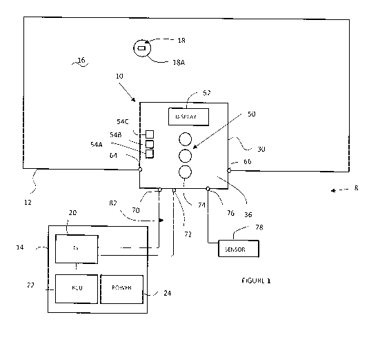
DESCRIPTION OF PREFERRED EMBODIMENT
[0027] Figure 1 of the accompanying drawings illustrates a part of a wireless
detonator
blasting system which includes apparatus 10 according to the invention which
is connected to
a loop antenna 12 at a blast site and to a transmitter arrangement 14. The
blasting system
may be implemented on surface, or at an underground location.
[0028] The loop antenna 12, which may comprise multiple turns, typically
encloses a blast site
of a large area 16 in which detonators 18 (only one detonator is shown), which
are wirelessly
operable, are placed in boreholes 18A drilled in the ground (only one
boreholes is shown). The
manner in which the boreholes are drilled and in which the detonators are
deployed is known
in the art and is not further described herein. The detonators are designed so
that, for example
in a unidirectional system, instructions and data from the transmitter
arrangement 14 can be
sent to the various detonators. In a bidirectional system information can be
sent in the reverse
direction i.e. from the detonators to the transmitter arrangement which would
then include an
appropriate receiver. These aspects are known in the art and for this reason
are not further
described herein.
[0029) The transmitter arrangement 14 includes a transmitter 20 and a blast
control unit 22
which controls the operation of the transmitter. The transmitter arrangement
also includes a
power source 24.
[0030] The antenna 12 is designed according to operational requirements. The
apparatus 10
is usable with a range of different antennas and to facilitate this aspect the
antennas are, where
possible, designed to have the same inductances. This allows antennas of
different sizes to
CA 03194040 2023-03-03
WO 2022/246481
PCT/ZA2022/050012
9
be used with the same apparatus 10. The size of the antenna is chosen
according to the
desired range of signal transmission.
[0031] The apparatus 10, which is portable, includes a housing 30, see Figure
3, which
consists of a base 32 and a closure 34 which is pivotally mounted to the base.
Components
of the apparatus which must be easily accessed during use of the apparatus 10
and which
facilitate operation of the apparatus are mounted on a surface 36 of the base.
Details of these
components are described hereinafter. When the closure 34 is moved to a closed
position it
overlies the various components on the surface 36 and thereby provides a
degree of physical
protection for these components and safety for operating personnel.
[0032] Referring to Figures 1 and 2, the apparatus 10 has mounted to or in the
housing 30, a
bank 38 of capacitors 40, a charging circuit 42, a measurement circuit 44, a
processor 46, a
memory unit 48, an array 50 of LEDs (light-emitting diodes), a display 52, a
communication
module 54, a battery 56 and an input module 60. The capacitors in the
capacitor bank 40 are
connected to antenna terminals 64 and 66. The antenna 12 is also connected to
these
terminals. The input module 60 is connected to input terminals 70 and 72. The
processor 46
is connected to a switch 74 which is accessible on the surface 36 of the
housing. One or more
contacts 76 are connectible, as required, to a plurality of sensors 78. The
sensors are chosen
according to requirement and typically are used to monitor parameters such as
temperature,
humidity, and time of operation of the apparatus, and to obtain an indication
of geographical
position of the apparatus through the use of a GPS,
[0033] If the apparatus is to be used with different antennas which have the
same inductance
values then it is conceivable that the capacitors 40 can be chosen to have a
set value. However
CA 03194040 2023-03-03
WO 2022/246481
PCT/ZA2022/050012
to allow for use of the apparatus with antennas which have different
inductance values the
bank 38 includes a plurality of capacitor modules 40A, 40B ... 40N. The
capacitance values
of the capacitors in each module are chosen so that substantially any desired
capacitance
value can be provided by selectively choosing the appropriate modules.
5 [0034] A switching circuit 80 is used together with the capacitor bank
38. As is explained
hereinafter the switching circuit 80 can be used manually by means of an
operator or
automatically via signals from the processor 46.
[0035] The apparatus 10 is used in the manner which has been described in the
preamble to
this specification. Thus the antenna 12 is deployed to enclose the area 16
which comprises a
10 blast site. The apparatus 10 is positioned at a location which is
relatively safe and secure and
protected against blasting effects. The antenna 12 is then connected to the
terminals 64 and
66. Thereafter the transmitter arrangement 14 is connected to the terminals 70
and 72 by
means of a suitable cable 82.
[0036] By activating the switch 74 a testing exercise is implemented. During
this process the
measurement circuit 44 in the apparatus is isolated from the high voltage
which is supplied
from the transmitter arrangement 14 to the apparatus 10 via the cable 82.
[0037] The measuring circuit 44 measures the inductance and capacitance of the
antenna 12.
These are known values and data relating thereto is stored in the memory unit
48. Any
meaningful deviation from the known values is indicative that the integrity of
the connections
made to the terminals 64 and 66 is suspect. The circuit 44 also measures the
integrity of the
connections made to the terminals 70 and 72. This is done in an appropriate
way for example
CA 03194040 2023-03-03
WO 2022/246481
PCT/ZA2022/050012
11
by measuring continuity in conductive lines on each side of the terminals 70,
72 ¨ continuity in
a line or terminal is readily ascertained by means of one or more resistance
value
measurements.
[0038] The measuring circuit 44 can also be used to measure the resistance of
the antenna
12 which is connected to the terminals 64 and 66. The resistance value of the
loop antenna is
generally known from previous measurements. That resistance value does not
change unless
some extraneous event has occurred. For example, the wires in the antenna may
be damaged
or may be affected by high temperature, moisture or humidity. The resistance
measurement
taken by the measuring circuit allows for these deviations to be handled. The
resistance
measurement can be taken directly from the antenna coil 12, as is indicated by
a line AC or
upstream of the contacts 64 and 66 as is indicated by means of a line marked
UC. The latter
measurement allows any change in the measured resistance, due to effects of
the connections,
to be detected.
[0039] The measurement data is collected by the processor 46 and stored in the
memory unit
48. An output of the data is available on the display 52. In one embodiment
the array 50 of
LEDs is fashioned so that if all the connections are in order a green LED is
illuminated. If
something is amiss a red LED is illuminated - this is a signal to an operator
that remedial action
must be taken.
[0040] In operation of the apparatus 10 the input module 60 conditions an
electrical supply
from the blast control unit 22, which draws power from the power source 24.
The charging
circuit 42 charges the capacitors 40 in the bank 38 to operating voltages.
These voltages are
sufficiently high to drive the antenna 12 so that it has a suitable range of
performance. The
CA 03194040 2023-03-03
WO 2022/246481
PCT/ZA2022/050012
12
battery 56 is powered and recharged by energy drawn from the input cable 82,
and is used to
power the processor 46, the array 50 of LEDs, and the display 52. To conserve
power the
LEDs and display are only energised when the switch 74 is operated.
[0041] The inductance measurement is additionally an indicator of good
deployment of the
antenna 12, for the inductance measurement is dependent on the size of the
area 16 enclosed
by the antenna. If the antenna is not satisfactorily deployed, for example if
it is folded, then the
inductance signal would be meaningfully affected.
[0042] The apparatus 10 has the capability, via the sensors 78, of collecting
data
(environmental or from any other cause) relating to factors which could have
an influence on a
blasting process. This data is stored in the memory unit.
[0043] The communication module 54 includes a number of ports which enable
information in
the memory module 48 to be downloaded. For example a near field communication
(NFC)-
enabled tagger can retrieve data via a port 54A (Figure 1), and Wi-fi and USB
connections can
be made via ports 54B and 540 respectively.
[0044] In one variation of the aforementioned process the inductance of the
loop antenna 12
is measured by the circuit 44. The processor 46, executing a program which is
based on the
use of known techniques, then calculates a capacitance value which should be
connected to
the antenna to achieve optimum performance. The display 52 is used to provide
a visual
indication of the capacitance value which is to be connected to the loop
antenna. An operator
can then choose from the modules 40A to 40N and via the switching circuit 80
ensure that
capacitors of the correct capacitance values are connected to the loop
antenna.
CA 03194040 2023-03-03
WO 2022/246481
PCT/ZA2022/050012
13
[0045] It is possible to automate the aforementioned process by suitably
designing the
switching circuit 80. In this instance the desired capacitance values are
calculated, in the
manner described, by the processor 46 and the switching circuit 80, in
response to signals
from the processor 46 then is actuated to connect a suitable selection of the
modules 40A to
.. 40N to the antenna coil.
[0046] In another approach the processor 46 causes the switching circuit 80 to
sweep through
various possible connections of groups of the capacitors so that the
capacitance value
connected to the loop antenna is gradually changed. For each stepped value the
degree of
tuning is determined by the measuring circuit and when an optimum value is
reached the
operator is notified via a suitable signal on the display 52.
[0047] Figure 2 also illustrates that power to the apparatus may be derived
from a mains
source 84. The energy from this source is used to charge the capacitors and to
charge the
battery 56. If the battery 56 is of adequate size then the battery, recharged
as appropriate, can
be used for the charging of the capacitors.