Note : Les descriptions sont présentées dans la langue officielle dans laquelle elles ont été soumises.
WO 2022/175770
PCT/IB2022/050865
DC power supply device and railway substation incorporating it
The present invention relates to a DC power supply device for supplying
direct current for the traction of trains, tramways and the like. According to
a
particular application, the DC power supply device is incorporated in a DC
railway
substation.
DC power supply devices generally include a rectifier connected to an AC
power distribution network via a transformer, with the rectifier being formed
of one
or more diode bridges. A drawback of such DC power supply devices is the drop
of DC line voltage as the load (e.g., vehicle power) increases, due to the
presence
of a series leakage reactance and a serial resistance. This voltage drop leads
to
the following issues:
- the spacing between substations must be limited to compensate voltage
drops;
- under heavy loads, the DC catenary voltage may drop excessively and,
as a consequence, the current may increase excessively, which causes
operational problems, such as dissipation, heat or circuit breaking, in
the power converters installed in the vehicle.
Thyristor rectifiers are gradually being adopted to address these issues in
new substation systems. Thyristor rectifiers allow controlling the DC voltage.
However, they are not exempt of drawbacks:
- existing traction-rectifier units need to be fully replaced;
- they are more expensive than diode rectifiers;
- they exhibit lower power factor.
Besides voltage drop issues, both diode rectifiers and thyristor rectifiers
exhibit unidirectional power flow, i.e., during braking events, the energy
flowing
through the DC line that cannot be captured by other trains needs to be wasted
in
large braking resistors. In order to address this limitation, regenerative
inverters,
either based on insulated-gate bipolar transistors (IGBTs) or thyristors, are
being
CA 03205529 2023- 7- 18
WO 2022/175770
PCT/IB2022/050865
2
incorporated to railway substations. Substations fitted with inverters are
called
reversible substations. A number of power electronics architectures for
reversible
substations are found in the state of the art, which can be mainly sorted
within
three groups:
- a diode
rectifier associated with an inverter, as disclosed in the patent
documents AU523146B, CN10277429B,
CN105226969B,
CN204333980U, EP3091631A1, EP234321361, CN102267405B and
CN202906763U;
- a thyristor rectifier associated with an inverter, as disclosed in the
article
"Efficient recovery of braking energy through a reversible DC
substation" by D. Comic, published in proc. of Electrical Systems for
Aircraft, Railway and Ship Propulsion Conference, 2010;
- bidirectional pulse width modulated (PWM) converters based on IGBTs,
see patent US 10554117.
The braking power is typically 25% to 30% of the motoring power. The large
difference of power levels in each power flow direction makes the use of diode
rectifiers combined with pulse width modulated (PWM) inverters, in particular
PWM inverters based on IGBTs, a suitable choice from a cost perspective.
Moreover, those allow retrofitting (i.e., the transformer-rectifier section
does not
need to be replaced). However, they still show limitations with respect to DC-
link
voltage controllability.
Some solutions, such as those disclosed in the patent documents
CN102774294B, CN102267405B and CN202906763U, propose to regulate the
DC voltage through active power injection, i.e., by sharing the active power
supplied to the DC line between the PWM inverter and the diode rectifier.
However, a high inverter power rating is required to mitigate the DC voltage
drop
across the entire operating range of the rectifier.
Another solution is proposed in the utility model CN 212323740 U, which
consists in compensating the reactive current and the harmonic current drawn
by
CA 03205529 2023- 7- 18
WO 2022/175770
PCT/IB2022/050865
3
the diode rectifier by providing reactive current and harmonic current of the
same
magnitude but opposite in phase. With this method, the DC voltage at the
output
side of the rectifier is necessarily stabilized at or near the no-load voltage
of the
rectifier, i.e. well above the nominal voltage of the rectifier, which
considerably
increases the inverter power rating required and thus the power consumption of
the inverter and reduces the overall energy efficiency of the system.
Moreover, this
method requires monitoring the reactive current and harmonics circulating at
the
AC terminals of the diode rectifier, thereby impacting the complexity and cost
of
the system, as this typically will require additional current and voltage
sensors.
The present invention aims at remedying the above-mentioned drawbacks
and provides to this end a DC power supply device comprising:
- a transformer having a primary side and a secondary side,
- a diode rectifier connected at its input side to the secondary side of
the
transformer,
- an inverter connected at its output side to the secondary side of the
transformer, and
- a controller arranged to control the inverter such that the inverter
generates reactive power and/or harmonics onto the secondary side of
the transformer so as to regulate the DC voltage at the output side of the
diode rectifier to a target value,
wherein the controller receives at its input side at least one DC signal
outputted by the diode rectifier and uses said at least one DC signal to
control the
inverter.
Particular embodiments of the invention are defined in the appended
dependent claims.
The present invention also provides a railway substation including the DC
power supply device defined above.
CA 03205529 2023- 7- 18
WO 2022/175770
PCT/IB2022/050865
4
Other features and advantages of the present invention will be apparent
upon reading the following detailed description made with reference to the
appended drawings in which:
- Figure 1 shows a DC power supply device according to the invention;
Figures 2 to 6 show different possible implementations of a
transformer, a diode rectifier and an inverter of the DC power supply
device according to the invention;
- Figure 7 shows a preferred implementation of the transformer, the
diode rectifier and the inverter of the DC power supply device
according to the invention;
- Figure 8 shows a closed-loop controller of the DC power supply device
according to the invention, which is arranged to control the inverter
such that the inverter generates reactive power to regulate the DC
output voltage of the diode rectifier;
Figure 9 shows the DC output voltage of the DC power supply device
versus load current in two cases: without the DC voltage regulation
according to the invention and with the DC voltage regulation
according to a first operating example of the invention;
- Figure 10 shows the response of the DC output voltage of the DC
power supply device when a train is in motoring operation, with the DC
voltage regulation according to the first operating example of the
invention and without the DC voltage regulation according to the
invention;
- Figure 11 shows another preferred implementation of the transformer,
the diode rectifier and the inverter of the DC power supply device
according to the invention;
- Figure 12 shows a closed-loop controller arranged to control the
inverter illustrated in Figure 11 such that the inverter generates both
CA 03205529 2023- 7- 18
WO 2022/175770
PCT/IB2022/050865
reactive power and harmonics to regulate the DC output voltage of the
diode rectifier;
Figure 13 shows simulation results of the DC output voltage of a DC
power supply device using the control method as disclosed in CN
5 212323740 U versus the DC load power of its diode rectifier
(curve
Cl), as well as simulation results of the DC output voltage of the DC
power supply device according to the invention versus the DC load
power of its diode rectifier in two cases: with the DC voltage regulation
according to a second operating example of the invention (curve C2)
and without the DC voltage regulation (curve C3);
Figure 14 shows simulation results of the apparent power of the
inverter of the said DC power supply device using the control method
as disclosed in CN 212323740 U versus the DC load power of its
diode rectifier (curve C4), as well as simulation results of the apparent
power of the inverter of the DC power supply device according to the
invention versus the DC load power of its diode rectifier in two cases:
with the DC voltage regulation according to the second operating
example of the invention (curve C5) and without the DC voltage
regulation (curve C6);
Figure 15 shows simulation results of the DC output voltage of the DC
power supply device according to the invention versus the DC load
power of its diode rectifier in two cases: with the DC voltage regulation
according to a third operating example of the invention (curve C7) and
without the DC voltage regulation (curve C8);
Figure 16 shows simulation results of the apparent power of the
inverter of the DC power supply device according to the invention
versus the DC load power of its diode rectifier in two cases: with the
DC voltage regulation according to the third operating example of the
CA 03205529 2023- 7- 18
WO 2022/175770
PCT/IB2022/050865
6
invention (curve C9) and without the DC voltage regulation (curve
C10);
- Figure 17 shows an alternative implementation of part of the controller
which controls the inverter in the DC power supply device according to
the invention, using as an input signal the DC rectifier output current
instead of the DC rectifier output voltage;
- Figure 18 shows a predetermined relationship between the DC rectifier
output current and a reactive power set point which can be used in the
implementation of Figure 17;
Figure 19 shows a predetermined relationship between the DC rectifier
output current, an AC voltage and a reactive power set point which
can be used in the implementation of Figure 17;
- Figure 20 shows another alternative implementation of part of the
controller which controls the inverter in the DC power supply device
according to the invention, using as input signals both the DC rectifier
output current and the DC rectifier output voltage.
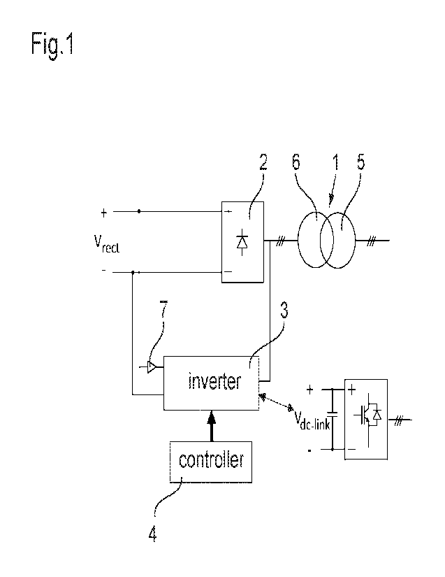
Referring to Figure 1, a DC power supply device according to the present
invention, for a DC railway substation, comprises a transformer 1, a diode
rectifier 2, an inverter (DC/AC converter) 3 and a controller 4. The primary
side 5
of the transformer 1 receives power from an AC distribution network, typically
a
three-phase AC distribution network, more particularly a three-phase medium-
voltage AC distribution network. The secondary side 6 of the transformer 1
delivers AC power to the input side of the diode rectifier 2. The diode
rectifier 2
outputs a DC voltage, Vrect, which is delivered to a railway line for the
traction of
trains. The inverter 3 receives at its input side the DC voltage Vrect and its
output
side is connected to the secondary side 6 of the transformer 1. One or more
diodes 7 at the input side of the inverter 3 makes the inverter 3
unidirectional. The
inverter 3 is preferably a pulse width modulated (PVVM) inverter, such as a
PVVM
inverter based on IGBTs, MOSFETs (Metal Oxide Semiconductor Field Effect
CA 03205529 2023- 7- 18
WO 2022/175770
PCT/IB2022/050865
7
Transistors) or IGCTs (Integrated Gate-Commutated Thyristors). Different
inverter
topologies can be used, including two-level inverters and multi-level
inverters.
During traction phases, the railway line is fed with the DC voltage Vrect
deriving from the AC distribution network through the transformer 1 and the
diode
rectifier 2 and the controller 4 controls the inverter 3 so that the DC
voltage Vrect is
regulated to a target value Vrect*, as will be explained later. During braking
phases,
the DC power generated by the braking of the train is converted by the
inverter 3
into AC power which is injected through the transformer 1 into the AC
distribution
network. This avoids the DC braking power being dissipated in the DC network
and enables a significant part of the traction power to be recovered.
Various implementations for the transformer 1, diode rectifier 2 and
inverter 3 are possible. As shown in Figures 2 to 6, the transformer 1 may be
a
delta-wye transformer and the diode rectifier 2 may comprise two diode bridges
8,
such as two six-pulse diode bridges, each connected to a respective one of the
secondary windings of the delta-wye transformer. The inverter 3 may include
(see
Figure 2) two three-phase power semiconductor bridges 9 receiving the DC
voltage Vrect through respective DC filters 10 and connected at their outputs
to the
two secondary windings, respectively, of the transformer 1 through respective
AC
filters 11. A tap in the secondary windings of the transformer 1 may be used
to
adjust the AC voltage level at the output side of the inverter 3. Instead of
using
taps, a transformer 12 (see Figure 3) or an auto-transformer 13 (see Figure 4)
may
be provided between each AC filter 11 and the corresponding secondary winding
of the transformer 1. Instead of having two power semiconductor bridges 9, the
inverter 3 may include a single three-phase power semiconductor bridge 9
receiving the DC voltage Vrect through a DC filter 10 and connected at its
output to
the secondary windings of the transformer 1 through a delta-wye transformer 14
and AC filters 11 (Figure 5) or through an autotransformer 15 and AC filters
11
(Figure 6).
CA 03205529 2023- 7- 18
WO 2022/175770
PCT/IB2022/050865
8
When one or more transformers 12, 14 are used at the output side of the
power semiconductor bridge(s) 9 (Figures 3 and 5), a single diode 7 is
sufficient at
the input side of the/each DC filter 10 due to the galvanic isolation provided
by the
transformers 12, 14. When no transformer or one or more autotransformers 13,
15
are used at the output side of the power semiconductor bridge(s) 9 (Figures 2,
4
and 6), two diodes 7 (one for each polarity + and -) are provided to avoid
recirculation.
The DC and AC filters 10, 11 include typically inductors and possibly
capacitors and resistors. Adaptation of voltage levels may be required on the
AC
side in order to prevent the inverter 3 from over-modulating. Such adaptation
can
be done by the transformers 12 (Figure 3), the autotransformers 13 (Figure 4)
or
the taps incorporated in the transformer 1 (Figure 2).
The architectures presented in Figures 2 to 4 can be adapted to a series
connection of rectifier diode bridges, which is typically found in 3000 Vdc
railway
networks. In this case, the inverter power semiconductor bridges 9 would be
connected in series rather than in parallel.
In Figure 7 is illustrated in more details an inverter 3 based on the
architecture of Figure 5 and having a two-level voltage source converter
topology.
In Figure 7, protections, contactors, pre-charge circuits, etc., are omitted
for the
sake of simplicity. The winding leakage inductances at the terminals of the
transformers 1, 14 are however shown and are used to perform the AC filter
duties. Additional AC filtering components (inductors, capacitors) could be
added
in series or parallel with the leakage inductances of the transformer 14 to
further
reduce the switching harmonics of the AC voltage at the output side of the
inverter
3. The key voltage and current measurements for control implementation are
shown, including the DC voltage Vrect, the DC link voltage Vdc _link at the
input of the
three-phase power semiconductor bridge 9 and at the output of the DC filter
10,
the AC currents ia, lb and ic at the output of the three-phase power
semiconductor
bridge 9, the AC voltages va, vi and ye at one secondary winding of the
CA 03205529 2023- 7- 18
WO 2022/175770
PCT/IB2022/050865
9
transformer 14 and the power semiconductor (here, IGBT) switching signals Qi
to
Q6.
Figure 8 illustrates a typical implementation of the controller 4, which here
is a closed-loop controller, based on a multi-loop control scheme. The
controller 4
includes a phase locked loop 20, an a-b-c to d-q transformation unit 21, a DC-
link
inverter control line 22 and a DC rectifier control line 23.
The phase locked loop 20 is tuned to set the "q" coordinate of the AC
voltage vci = 0 and converts the three-phase voltages Va, Vb and vb into a
voltage
magnitude Vd, a phase angle 0 and an angular frequency w.
The a-b-c to d-q transformation unit 21 converts the three-phase currents ia,
ib and ib into two components id and iq in a synchronous reference frame (d-q
frame) using the phase angle B.
The function of the DC-link inverter control line 22 is known per se. It
consists in regulating the DC link voltage Vdc_iink so that the power
semiconductor
bridge 9 receives a sufficient voltage for its operation. The DC-link inverter
control
line 22 includes a DC voltage closed-loop controller 24 comprising, in series,
a
subtractor 25 which subtract a target value Vdc _fink* from the inverter DC
link
voltage Vdb_link and a proportional-integral (PI) compensator 26 which outputs
an
active power set point P*. The DC-link inverter control line 22 further
includes an
AC current closed-loop controller 27 comprising, in series, a scaling unit 28
for
converting the active power set point P* into a reference current id* using
the AC
voltage magnitude Vd, a subtractor 29 for subtracting the actual current id
output by
the a-b-c to d-q transformation unit 21 from the reference current id*, a
proportional-integral compensator 30, another subtractor 31 for subtracting
the
voltage w.L.ici from the voltage output by the proportional-integral
compensator 30,
where L is the equivalent AC inductance seen from the output side of the
inverter
3, and an adder 32 which adds the output signal of the subtractor 31 to the
voltage
magnitude Vd delivered through a scaling unit 42 to output a voltage command
Vid
for the inverter 3.
CA 03205529 2023- 7- 18
WO 2022/175770
PCT/IB2022/050865
The DC rectifier control line 23 includes a DC voltage closed-loop
controller 33 comprising, in series, a subtractor 34 which subtracts the
rectifier DC
voltage Vrect from a target value Vrect* and a proportional-integral (PI)
compensator
35 which outputs a reactive power set point Q*. The DC rectifier control line
23
5 further includes an AC current closed-loop controller 36 comprising, in
series, a
scaling unit 37 for converting the reactive power set point Q* into a
reference
current ici* using the AC voltage magnitude Vd, a subtractor 38 for
subtracting the
actual current iq output by the a-b-c to d-q transformation unit 21 from the
reference current ici*, a proportional-integral compensator 39, and an adder
40 for
10 adding the voltage output by the proportional-integral compensator 39 to
the
voltage w.L.id, where L is the equivalent AC inductance seen from the output
side
of the inverter 3, so as to output a voltage command Viq for the inverter 3.
The voltage commands Vid and Viq are input into a pulse width modulator 41
together with the phase angle O. The pulse width modulator 41 outputs the
switching signals Qi to Q6 to control the power semiconductor bridge 9 of the
inverter 3. The pulse width modulator 41 may implement different known
modulation schemes, such as Space Vector Modulation, Sinusoidal Modulation, a
type of Discontinuous Pulse Width Modulation or others.
When the train is motoring, the inverter 3 cannot provide power to the DC
network due to the presence of the blocking diode 7. The inverter DC link
voltage
Vdc _link is indeed higher than the rectifier DC voltage Vrect (i.e.,
Vdc_iink* > Vrect*) so
that the diode 7 is in the blocking condition. The compensator 26 drives the
active
power set point P* to a small value which allows compensating power losses of
the inverter 3.
When the train is braking, the active power set point P* is set to the total
regenerated power generated from the DC network into the AC network. In this
scenario, the diode 7 starts conducting and Vrect Vdc_link.
As regards the DC rectifier control, when the train is motoring the
compensator 35 drives the reactive power set point Q* such that Vrect is
regulated
CA 03205529 2023- 7- 18
WO 2022/175770
PCT/IB2022/050865
11
to a target value Vrect*. When the train is braking, Vrect increases beyond a
certain
limit of voltage control and Q* is set to zero.
The AC current closed-loop controllers 27, 36 enable to regulate the power
factor of the AC current at the output of the inverter 3. The AC current
closed-loop
controllers 27, 36 are useful in both modes of operation (train motoring and
train
braking) but control implementations without such inner AC current closed loop
are
also possible.
Figure 9 shows the rectifier DC voltage Vrect as a function of load current
(i.e. DC current consumed at the output side of the diode rectifier 2 by the
DC
network, a load current of 100% corresponding to the nominal DC current)
without
the DC voltage regulation according to the invention (inverter 3 disabled;
continuous line in the diagram of Figure 9) and with the DC voltage regulation
according to the invention (inverter 3 and DC rectifier control line 23
enabled;
dashed line in the diagram of Figure 9). As can be seen, in the absence of the
DC
voltage regulation, the voltage drops as the load current increases, which
causes
the current to increase for a given power value and to generate dissipation,
heat
and risk of circuit breaking. When the inverter 3 is enabled, the DC rectifier
control
line 23 causes the inverter 3 to generate reactive power onto the secondary
side
of the transformer 1 so that the DC voltage Vrect is regulated to a target
value,
which can be either constant or varied depending on load current. In the shown
diagram, the DC voltage Vrect starts being regulated at a load current of 10%
and is
gradually reduced down to 750 V, which is the nominal voltage of the diode
rectifier 2 and of the DC network, at a load current of 50%. Beyond 50%, the
DC
voltage is maintained regulated to 750 V. The inverter DC-link voltage
Vdc_link is
then regulated through the active power set point P*.
The present invention thus has the advantage of using a cheap, reliable and
long-lifetime rectifier, i.e., the diode rectifier 2, without suffering from
the DC
voltage drop which diode rectifiers normally exhibit when combined with a
transformer.
CA 03205529 2023- 7- 18
WO 2022/175770
PCT/IB2022/050865
12
In comparison with existing solutions for DC voltage regulation based on
active power generation, an advantage of the present invention is the reduced
power rating required for the inverter 3 to achieve regulation of the
rectifier
voltage. Indeed, reactive power is normally not useful in a DC power supply
device. The present invention uses the reactive power circulating in the AC
section
of the device for the purpose of regulating the rectifier DC voltage.
Moreover, the unidirectional character of the inverter 3 makes it possible for
the inverter 3 to have small dimensions since it can be dimensioned only for
the
regenerative power rather than for the total power. Inverters typically
require a
power rating ranging from 25% to 30% of the rectifier power for braking energy
recovery purposes. In the present invention, the inverter 3 can be dimensioned
only for the regenerative power and there is no need to increase the power
rating
of the inverter for voltage regulation purposes.
Simulation results are presented in Figure 10. The nominal voltage of the
diode rectifier 2 and of the DC network is 750 V and the nominal power of the
diode rectifier 2 is 3 MW. The railway network power is gradually stepped from
50% up to 300% (a load of 100% corresponding to the nominal power). When the
inverter 3 is disabled, the rectifier voltage drops from 765 V down to 665 V.
When
the inverter 3 is enabled with the reactive power controller activated, the
rectifier
voltage is kept regulated to 750 V under all power levels. Up to a load power
of
about 100%, the inverter 3 generates some level of inductive power (reactive
power with negative sign). As the load power increases beyond 100%, the
inverter
3 generates capacitive power (reactive power with positive sign). The higher
the
level of rectifier voltage compensation, the higher the reactive power
required.
It will be clearly apparent to a person skilled in the art that many
modifications can be made in the embodiment of Figure 8. For example, in the
DC
voltage closed-loop controller 24, 33 of the DC-link inverter control line 22
and/or
of the DC rectifier control line 23, components based on PID (proportional-
integral-
derivative) compensators, model predictive control, etc., could be used
instead of
CA 03205529 2023- 7- 18
WO 2022/175770
PCT/IB2022/050865
13
proportional-integral compensators. The AC current closed-loop controller 27,
36
could use other control loop solutions than the one disclosed above, e.g.,
stationary frame control or hysteresis control. In addition, the reactive
power set
point range could be limited only to positive values ¨ the dashed line in
Figure 9
would then follow the continuous line for load currents between 0 and 100% ¨
so
as to perform only boosting of the rectifier DC voltage Vrect.
The regulation function fulfilled by the present invention can be
complemented with a harmonics compensation function in order to further reduce
the amount of current required from the inverter 3 to regulate Vrect. In this
case, the
rectifier DC voltage Vied can be increased by compensating (partially or
totally) the
current harmonics drawn by the diode rectifier 2 which, similarly to the
reactive
power, also generate a voltage drop in the transformer 1. The required level
of
compensation can be commanded by a DC voltage closed-loop controller similar
to the controllers 24, 33, or can be set for maximum compensation. The
compensation of harmonics can be carried out using existing techniques applied
for active power filtering, such as modulation schemes based on selective
harmonic cancellation methods as disclosed in the article by I. Quesada et al.
entitled "Evaluation of the boundaries of the solutions space for the Harmonic
Cancellation Technique", Przeglad Elektrotechniczny, vol. 88, no. la, pp. 21-
25,
2012 or based on current control schemes with harmonics compensation networks
as disclosed in the article by L. Limongi et al. entitled "Digital Current-
Control
Schemes", IEEE industrial Electronics Magazine, vol. 3, no. 1, 2009.
An implementation example of the harmonics compensation method
combined with the rectifier output voltage control method is described below.
Figure 11 shows a detailed implementation of an architecture that uses the AC
interconnection concept shown in Figure 3. This includes a transformer 1, a
diode
rectifier 2 with two six-pulse diode bridges 81, 82 and an inverter 3 with two
IGBT
inverter bridges 91, 92. The IGBT inverter bridges 91, 92 are respectively
interconnected with the diode bridges 81, 82 through transformers 121, 122. In
this
CA 03205529 2023- 7- 18
WO 2022/175770
PCT/IB2022/050865
14
example, the current measurement signals i
=a,b,c and switching command signals
C21-6 of the IGBTs of each inverter bridge 91, 92 are controlled separately.
Signals
with sub-index "1" correspond to the inverter bridge 91, and signals with sub-
index
"2" correspond to the inverter bridge 92. The input currents to the rectifier
diode
bridges 81, 82 are labelled as i .al_rect, ibl_rect, icl_rect, la2_rect,
ib2_rect, ic2_rect, and the DC
output current of the diode rectifier 2 is labelled as .dc_rect.
Figure 12 shows an implementation of the controller 4 based on current
control for the harmonics compensation method combined with the rectifier
output
voltage control method. The controller 4, here a closed-loop controller,
includes
units 20, 25, 26, 28, 34, 35, 37 similar to the corresponding units in Figure
8. The
input rectifier currents i .al_rect, ibl_rect, icl_rect at the first diode
bridge 81 are measured
and inputted to a harmonics compensation reference calculation unit 431. This
unit
431 incorporates a transformation from a-b-c frame to d-q frame and filtering
functions. The unit 431 outputs two reference signals i .dl_rect_h* and i
.ql_rect_h* that will
include the harmonics of the diode bridge 81 to be compensated by the
controller 4
with their sign adapted (the fundamental component is filtered out). The three-
phase currents .al, .bl, .c1 o.f the first inverter bridge 91 are converted by
an a-b-c to
d-q transformation unit 211 into two components Idi, ico in a synchronous
reference
frame.
In an adder/subtractor 291 the signal idl is subtracted from the sum of the
reference signal i .dl_rect_h* and the reference signal id* coming from the
scaling unit
28. A dedicated harmonic compensator 441 is typically added in parallel to a
proportional-integral compensator 301 similar to the compensator 30 in Figure
8 in
order to enhance the compensation capabilities of the current controller 4 at
the
targeted harmonic frequencies. The signal w.L.igi is subtracted from the sum
of
the outputs of units 441 and 301 in an adder/subtractor 311 and the result is
provided to an adder 321 which adds it to the output of a scaling unit 421
receiving
the voltage Vd output by the phase-locked loop 20. The adder 321 outputs a
voltage command Vidl.
CA 03205529 2023- 7- 18
WO 2022/175770
PCT/IB2022/050865
In an adder/subtractor 381 the signal i q1 is subtracted from the sum of the
reference signal i .qtrect_h* and the reference signal iq* coming from the
scaling unit
37. A dedicated harmonic compensator 451 is typically added in parallel to a
proportional-integral compensator 391 similar to the compensator 39 in Figure
8 in
5 order to enhance the compensation capabilities of the current controller
4 at the
targeted harmonic frequencies. The signal w.L.idi and the outputs of units 451
and
391 are added by an adder 401 to produce another voltage command Viq1. The
voltage commands Vidi and Viqi are provided to a pulse width modulator 411
together with the phase angle 0 output by the phase-locked loop 20. The pulse
10 width modulator 411 outputs the switching signals Q11, Q21, 031, Q41,
Q51, Q61 to
control the first inverter bridge 91.
The same units as 211, 431, 291, 301, 441, 311, 321, 421, 381, 391, 401, 451
are provided for the three-phase currents ia2, .lb2, .l c2 O. f the second
inverter bridge 92
.
and the input rectifier currents i .a2_rect, ib2_rect, ic2_rect at the second
diode bridge 82
15 and shown as a single block 462 for the sake of simplicity. Voltage
commands Vid2
and Viq2 are thus produced and provided to a pulse width modulator 412
together
with the phase angle 61 output by the phase-locked loop 20. The pulse width
modulator 412 outputs the switching signals 012, Q22, Q32, Q42, Q52, 062 to
control
the second inverter bridge 92.
The harmonic compensators 441, 451 (and those of block 462) may be
based on resonant compensators resonating at 6 f -.fund (which compensates the
negative sequence of the 5th harmonic and the positive sequence of the 7th
harmonic), and possibly other frequencies such as 12 f ..fund etc., where
ffund is the
fundamental frequency. As a result, the inverter voltage commands Vid and Viq
are
modulated so that the inverter AC current partially compensates the rectifier
AC
current harmonics. Other implementations for harmonics compensation based on
multiple synchronous reference frames and other schemes are also possible
(refer
to article by Limongi et. Al. "Digital Current-Control Schemes", IEEE
industrial
Electronics Magazine, vol. 3, no. 1, 2009).
CA 03205529 2023- 7- 18
WO 2022/175770
PCT/IB2022/050865
16
One will note that instead of being added to the control lines 22, 23 as is
done in the embodiment of Figure 12, the compensation of harmonics may replace
the DC rectifier control line 23, i.e., a control line similar to the control
line 23 in
Figure 8 may be used but for generating harmonics instead of reactive power,
the
harmonics being generated for the purpose of regulating the rectifier DC
voltage
Vrect.
As is apparent, in the embodiments of the invention described above the
controller 4 receives the DC voltage Vrect as an input and uses this voltage
as a
feedback signal to control the inverter 3 so as to regulate the DC voltage
Vrect to a
target value Vrect*. The target value Vrect* may be constant or may vary as a
function of the load current. In the latter case, a conventional DC current
sensor
placed at the output side of the diode rectifier 2 may provide DC load current
data
to the controller 4 to enable the controller 4 to vary the target value Vrect*
according
to a predetermined rule.
By using the DC voltage as a feedback signal inputted into the controller 4,
the present invention has the advantage, with respect to the device disclosed
in
CN 212323740 U, of not requiring an expensive sensing scheme including voltage
and current sensors at the input (AC side) of the diode rectifier to measure
its
reactive power and harmonics in order to compensate them.
Moreover, as is shown by the simulation curve Cl in Figure 13, the DC
voltage in the device disclosed in CN 212323740 U is maintained near the no-
load
voltage (about 790 V in Figure 13) and thus well above the nominal voltage
(750 V) because it is regulated over the entire operating range of the diode
rectifier
by fully compensating the reactive power and harmonics drawn by the diode
rectifier. This results in a high power consumption by the inverter (see
Figure 14,
curve C4). It is specified that for the simulation of the device disclosed in
CN
212323740 U, an interphase transformer was incorporated between the DC
positive terminals of the rectifier bridges since otherwise the amount of the
5th and
CA 03205529 2023- 7- 18
WO 2022/175770
PCT/IB2022/050865
17
7th harmonics in the AC current circulating between the inverter and the diode
rectifier was excessive.
On the other hand, in the present invention (see Figure 13, curve C2), the
controller 4 may control the inverter 3 such that:
the inverter 3 is inactive when the DC voltage Vred falls from the no-
load voltage of the diode rectifier 2 to the nominal voltage of the diode
rectifier 2 (750 V in the example),
the inverter 3 becomes active when the DC voltage Vrect reaches the
nominal voltage of the diode rectifier 2 to regulate said DC voltage to
said nominal voltage across the operating range of the diode rectifier 2
from the nominal power (3000 kW in the example) to the maximum
overload (300% of nominal power in the example).
In this manner, the power consumed by the inverter is much reduced (see
Figure 14, curve C5) and the global energy efficiency and equipment lifetime
are
increased. In particular, the power rating of the inverter 3 does not need to
be
higher than what is required for energy recovery, and the inverter 3 only
needs to
be operated when the DC voltage drops below the nominal voltage level.
In Figures 13 and 14 has also been shown for comparison the evolution of
the DC voltage Vred and of the apparent power of the inverter 3 when the
inverter 3 is disabled (curves C3 and C6).
In the example of Figures 13 and 14, like in the example shown in Figures 9
and 10, only reactive power is generated by the inverter 3 of the DC power
supply
device according to the invention to regulate the DC voltage Vred. However,
unlike
in the example shown in Figures 9 and 10 where inductive power is generated
before the 100% load to start the regulation, the reactive power in the
example of
Figures 13 and 14 is only capacitive and generated as from the 100% load.
Figures 15 and 16 show another operating example of the DC power supply
device according to the invention. In this example (see curve C7), the diode
rectifier is assumed to have a maximum overload capacity of 450%. The DC
CA 03205529 2023- 7- 18
WO 2022/175770
PCT/IB2022/050865
18
voltage Vrect is regulated to the nominal voltage across the operating range
from
the nominal load power to e.g. 300% load power and then is regulated to a
target
value which is lower than the nominal voltage but remains higher than the DC
voltage without regulation (see curve C8) and which decreases as a function of
load power. In particular, as shown, the varying target value may be chosen so
that the voltage drop compensation remains constant beyond 300% load power
and up to the maximum overload, i.e. 450%, thereby enabling the power
consumption of the inverter 3 to be clamped (see curve C9) so that the
inverter 3
does not need to be over-dimensioned only for the purpose of regulating the DC
voltage.
Regulating the DC voltage Vrect to the nominal voltage of the diode
rectifier 2 and starting the regulation at the nominal voltage are preferred
for
simplicity and energy efficiency reasons. However, in alternative embodiments,
the
regulation may start at a predetermined value for the DC voltage Vrect which
is
lower than the no-load voltage of the diode rectifier 2 but different from
(higher or
lower than) the nominal voltage.
In general manner, in the present invention the regulation may start when
the DC voltage Vrect, falling from the no-load voltage of the diode rectifier
2,
reaches a predetermined voltage (equal to or different from the nominal
voltage),
with the DC voltage Vrect being regulated to a constant or varying target
value that
is equal to or lower than the predetermined voltage. The difference between
the
no-load voltage and the predetermined voltage is typically at least 25%,
preferably
at least 50%, preferably at least 75% of the difference between the no-load
voltage
and the nominal voltage of the diode rectifier 2. The difference between the
no-
load voltage and the predetermined voltage is typically at most 125%,
preferably at
most 110% of the difference between the no-load voltage and the nominal
voltage
of the diode rectifier 2.
In all embodiments described above, the controller 4 controls the inverter 3
using the DC voltage Vrect as a feedback signal. In other embodiments,
however,
CA 03205529 2023- 7- 18
WO 2022/175770
PCT/IB2022/050865
19
the controller 4 may control the inverter 3 using the DC current outputted by
the
diode rectifier 2 instead of, or in addition to, the DC voltage Vrect. Figure
17 shows
such an embodiment, in which the DC voltage closed-loop controller 33 of
Figure 8
or the corresponding DC voltage closed-loop controller of Figure 12 is
replaced
with a look-up table or analytical function 47 which modulates the reactive
power
set point Q* as a function of the DC rectifier output current idc_red using a
predetermined relationship between the DC rectifier output current and the
reactive power set point. This input-output relationship is calculated aiming
to
compensate the voltage drop at the DC side caused by an increase of the DC
rectifier output current, and can take also the AC voltage Vd as an input.
Figures
18 and 19 show two examples of input-output relationship implementations based
on a simple linear approach. The example of Figure 18 takes only the DC
rectifier
output current as an input. The example of Figure 19 takes both the DC
rectifier
output current and the AC voltage as inputs. The regulation of the DC voltage
using the DC rectifier output current instead of the DC voltage itself is less
accurate because the relationship between reactive power injection, AC
voltage,
DC voltage and DC current is based on a model, i.e. there is no closed-loop
control action that compensates the difference between the target DC voltage
level
and the measured DC voltage level. However, such a regulation also has great
advantages:
- it has a higher control bandwith: the response time is basically defined
by the inner current loop of the inverter;
- it is simpler: there is no need to tune the outer control loop, thus
avoiding potential stability issues;
- it does not require a DC rectifier voltage sensor.
A combination of both techniques may be used, so that the DC current
measurement allows accelerating the response time of the system while the DC
voltage closed-loop control performs a fine adjustment of the reactive power
set
CA 03205529 2023- 7- 18
WO 2022/175770
PCT/IB2022/050865
point to control the voltage exactly to the targeted level. Figure 20
illustrates an
implementation that integrates both methods.
5
CA 03205529 2023- 7- 18