Note : Les descriptions sont présentées dans la langue officielle dans laquelle elles ont été soumises.
CA 03212659 2023-09-06
WO 2022/192319
PCT/US2022/019430
- 1 ¨
FLUORINATED ELASTOMERS FOR BRAIN PROBES AND OTHER
APPLICATIONS
RELATED APPLICATIONS
This application claims priority to U.S. Provisional Application No.
63/159,623,
filed March 11, 2021, and entitled "Perfluorinated Elastomers for Brain Probes
and
Other Applications"; and to U.S. Provisional Application No. 63/290,732, filed
December 17, 2021, and entitled "Fluorinated Elastomers for Brain Probes and
Other
Applications," which are each incorporated herein by reference in their
entirety for all
purposes.
TECHNICAL FIELD
Articles and methods related to fluorinated elastomers are generally
described.
BACKGROUND
Decoding neural signals is of fundamental importance to bridge the existing
gap
of knowledge between our molecular understanding of synaptic circuits and
behavioral
neurosciences. Understanding neurodegenerative diseases or brain circuitry in
general,
and increasing the bandwidth of brain-machine interfaces for novel medical
devices such
as neuroprostheses or deep brain stimulators, are, to name a few, potential
applications
that would benefit from advanced neural interface technologies. However,
probing the
dynamic of neural network on a sufficiently large spatial and temporal scale
to
understand neural encoding requires simultaneous measurements on tens, if not
hundreds
of thousands of neurons, in vivo, over time. Moreover, each neuron itself can
have tens
to hundreds of thousands of synaptic connections, which can extend throughout
the
entire volume of the brain. Therefore, chronically stable and brain-wide
activity
mapping is needed to understand the connectome of the brain.
Various microelectrode array technologies have been developed to measure
single-unit extracellular action potentials of hundreds to thousands of
neurons
simultaneously and over period of times extending from weeks to months.
Nevertheless,
further increasing the density of electrical sensors, such as microelectrodes
or transistors,
has been limited by the immune response caused by the mechanical mismatch
between
the probes and the brain tissues. Accordingly, improvements are needed.
SUMMARY
CA 03212659 2023-09-06
WO 2022/192319
PCT/US2022/019430
¨ 2 ¨
Articles and methods related to fluorinated elastomers are generally
described.
The subject matter of the present invention involves, in some cases,
interrelated products,
alternative solutions to a particular problem, and/or a plurality of different
uses of one or
more systems and/or articles.
One aspect is generally directed towards an article. According to some
embodiments, the article comprises: a first layer comprising a first
fluorinated polymer; a
second layer, bonded to the first layer; and a third layer, bonded to the
second layer,
comprising a second fluorinated polymer.
Another aspect is generally directed towards an article. In some embodiments,
the article comprises: a substrate configured to be implanted into an organ of
a subject,
the substrate comprising a plurality of electrodes, the substrate comprising a
first layer
comprising a first fluorinated polymer, a second layer bonded to the first
layer, and a
third layer comprising a second fluorinated polymer bonded to the second
layer.
Yet another aspect is generally directed towards an article. In some
.. embodiments, the article comprises: a substrate comprising a plurality of
electrodes, the
substrate comprising a first layer comprising a first fluorinated polymer, a
second layer
bonded to the first layer, and a third layer comprising a second fluorinated
polymer
bonded to the second layer, a ratio of to greater or equal to 10-9
electrodes/micron2
Still another aspect is generally directed towards an article. In some
embodiments, the article comprises: a substrate comprising a plurality of
electrodes, the
substrate comprising a first layer comprising a first fluorinated polymer, a
second layer
bonded to the first layer, and a third layer comprising a second fluorinated
polymer
bonded to the second layer, wherein the electrodes have a number density
greater than or
equal to 10-3 electrodes/micron2.
Another embodiment is generally directed towards an article. In some
embodiments, the article comprises: a substrate comprising a plurality of
electrodes, the
substrate comprising a first layer comprising a first fluorinated polymer, a
second layer
bonded to the first layer, and a third layer comprising a second fluorinated
polymer
bonded to the second layer, wherein the substrate has an overall elastic
modulus of less
than or equal to 106 Pa.
Yet another aspect is generally directed towards an article. According to some
embodiments, the article comprises: a first layer comprising a first
fluorinated polymer; a
CA 03212659 2023-09-06
WO 2022/192319
PCT/US2022/019430
¨ 3 ¨
second layer, bonded to the first layer; and a third layer, bonded to the
second layer, and
comprising a second fluorinated polymer; wherein the third layer has an
average
thickness H in microns, wherein the polymer on the substrate exhibits a
reduction in
specific electrochemical impedance modulus (i.e., the electrochemical
impedance
modulus, normalized to the geometry of the sample) at 1 kHz of no more than
50% after
being immersed for in 10x PBS solution at 65 C for a period of time of at
least 1*H2
days.
One aspect is generally directed to an article, comprising a first layer
comprising
perfluoropolyether; a second layer, bonded to the first layer; and a third
layer, bonded to
the second layer, comprising perfluoropolyether.
Another aspect is generally directed to an article, comprising a
perfluoropolyether
having a weight-average molecular weight of less than 8 kDa, wherein the
perfluoropolyether is on a semiconductor substrate.
Yet another aspect is generally directed to an article, comprising a polymer,
comprising a cross-linked perfluoropolyether, on a substrate, wherein the
polymer, when
formed into an article having a minimum dimension of at least 0.3 micrometers
that is
immersed in 1,3-bis(trifluoromethyl)benzene for a period of greater than or
equal to 9
seconds, dried in nitrogen, and measured at 1 kHz, exhibits a specific
electrochemical
impedance modulus of at least 106 ohm-m.
Still another aspect is generally directed to an article, comprising a
polymer,
comprising a cross-linked perfluoropolyether, on a substrate, wherein the
polymer on the
substrate exhibits a reduction in specific electrochemical impedance modulus
at 1 kHz of
no more than 50% after being immersed for 100 days in phosphate buffer
solution.
Another aspect is generally directed towards a method. In some embodiments,
the method comprises: inserting, into an organ of a subject, a substrate
comprising a
plurality of electrodes, the substrate comprising a first layer comprising a
first fluorinated
polymer, a second layer bonded to the first layer, and a third layer
comprising a second
fluorinated polymer bonded to the second layer.
Still another aspect is generally directed towards a method. In some
embodiments, the method comprises: depositing a fluorinated polymer on a
substrate;
applying an inert gas plasma to the fluorinated polymer to form a treated
fluorinated
polymer; and depositing a material onto the treated fluorinated polymer.
CA 03212659 2023-09-06
WO 2022/192319
PCT/US2022/019430
¨ 4 ¨
Yet another aspect is generally directed towards a method. In some
embodiments, the method comprises: depositing a fluorinated polymer on a
substrate;
treating the fluorinated polymer to render it susceptible to deposition; and
depositing a
second fluorinated polymer onto the treated fluorinated polymer.
One aspect is generally directed towards a method. In some embodiments, the
method comprises: depositing a fluorinated polymer on a substrate; treating
the
fluorinated polymer to render it susceptible to deposition; depositing a
material forming
a plurality of electrodes onto the treated fluorinated polymer.
Another aspect is generally directed towards a method. In some embodiments,
the method comprises: determining electrical signals from a plurality of
electrodes on a
substrate at least partially contained within a subject, wherein the substrate
comprises a
first layer comprising a first fluorinated polymer, a second layer bonded to
the first layer,
and a third layer comprising a second fluorinated polymer bonded to the second
layer.
Still another aspect is generally directed towards a method. In some
embodiments, the method comprises: determining electrical activity of a single
cell
within a living subject using an electrode on a substrate in contact with the
cell over at
least 5 days, wherein the substrate comprises a layer comprising a fluorinated
polymer.
Yet another aspect is generally directed towards a method. In some
embodiments, the method comprises: determining electrical signals from a
plurality of
electrodes on a substrate at least partially contained within a subject,
wherein the
substrate has an overall elastic modulus of less than or equal to 106 Pa and
comprises a
layer comprising a fluorinated polymer.
One aspect is generally directed towards a method. In some embodiments, the
method comprises: electrically stimulating cells within a subject using a
plurality of
electrodes on a substrate, wherein the substrate comprises a first layer
comprising a
fluorinated polymer, a second layer bonded to the first layer, and a third
layer comprising
a fluorinated polymer bonded to the second layer.
Another aspect is directed to a method, comprising depositing
perfluoropolyether
on a substrate; applying an argon plasma to the perfluoropolyether to form a
treated
.. perfluoropolyether; and depositing a material onto the treated
perfluoropolyether.
Other advantages and novel features of the present invention will become
apparent from the following detailed description of various non-limiting
embodiments of
CA 03212659 2023-09-06
WO 2022/192319
PCT/US2022/019430
¨ 5 ¨
the invention when considered in conjunction with the accompanying figures. In
cases
where the present specification and a document incorporated by reference
include
conflicting and/or inconsistent disclosure, the present specification shall
control.
BRIEF DESCRIPTION OF THE DRAWINGS
Non-limiting embodiments of the present invention will be described by way of
example with reference to the accompanying figures, which are schematic and
are not
intended to be drawn to scale unless otherwise indicated. In the figures, each
identical or
nearly identical component illustrated is typically represented by a single
numeral. For
purposes of clarity, not every component is labeled in every figure, nor is
every
component of each embodiment of the invention shown where illustration is not
necessary to allow those of ordinary skill in the art to understand the
invention. In the
figures:
FIG. 1 presents a cross-sectional schematic illustration of an exemplary
article
comprising a perfluorinated polymer, according to certain embodiments;
FIG. 2 presents a cross-sectional schematic illustration of an experimental
setup
for measuring impedance, according to certain embodiments;
FIG. 3 presents a method of preparing an article comprising a perfluorinated
polymer, according to certain embodiments;
FIGS. 4A-4D present specific electrochemical impedance measurements of
polymer films, according to certain embodiments;
FIG. 5A presents an illustrated method of determining ion concentration of a
polymer, according to certain embodiments;
FIG. 5B present exemplary concentration profiles of ions after exposing a
polymer that had previously equilibrated with a buffer to deionized water;
FIGS. 5C-5D compare the ion desorption of polymer layers at various
temperatures, according to certain embodiments;
FIG. 5E compares the ionic conductivity of polymer layers determined by
different measurements, according to certain embodiments;
FIG. 6 presents an equation used to determine ionic conductivity, according to
certain embodiments;
FIGS. 7A-7C compare the temperature dependence of ion behavior within
polymers, according to certain embodiments;
CA 03212659 2023-09-06
WO 2022/192319
PCT/US2022/019430
¨ 6 ¨
FIG. 8 presents an exemplary method of preparing an article comprising a
perfluorinated polymer, according to certain embodiments;
FIGS. 9A-9B present an exemplary nitrogen diffuser, according to certain
embodiments;
FIG. 10A compares the specific electrochemical impedance modulus of
polymers, according to certain embodiments;
FIG. 10B presents mechanical properties of polymers, according to certain
embodiments:
FIG. 10C compares the elastic modulus with the electrochemical stability of
polymer materials, according to certain embodiments;
FIGS. 11A presents an exploded perspective illustration of an exemplary
article
designed for use as a neural sensor, according to certain embodiments;
FIGS. 11B-11E present images of exemplary article designed for use as a neural
sensor, according to certain embodiments;
FIGS. 12A-12B present the resistance of metal electrodes, according to certain
embodiments;
FIGS. 13A-13B compare impedance behavior of articles comprising uncorrected
electrodes and electrodes coated with PEDOT:PSS, according to certain
embodiments;
FIG. 14 presents a photograph of a plastic frame used to hold a device,
according
to certain embodiments;
FIGS. 15A-15B present the insertion of a device into the brain of a living,
moving mouse, according to certain embodiments;
FIGS. 16A-16E present the signal collected from a device implanted into the
brain of a living mouse;
FIGS. 17A-17C present specific electrochemical impedance measurements of
polymer films, according to certain embodiments;
FIG. 18 presents a method of preparing an article comprising a fluorinated
polymer, according to certain embodiments;
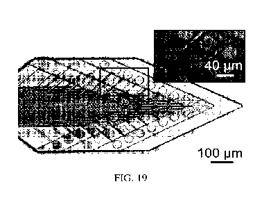
FIG. 19 presents an image of an exemplary article designed for use as a neural
sensor, according to certain embodiments;
FIG. 20 presents a change in electrochemical impedance modulus of an electrode
upon coating with conductive materials, according to some embodiments;
CA 03212659 2023-09-06
WO 2022/192319
PCT/US2022/019430
¨ 7 ¨
FIG. 21 presents the change in electrochemical impedance modulus of polymers
on exemplary electrodes over time, according to some embodiments;
FIG. 22 compares electrode number density and elastic modulus for various
neural sensors, with neural sensors prepared according to the embodiments
described
herein, according to some embodiments;
FIG. 23 presents a schematic illustration of an exemplary peel test, according
to
some embodiments;
FIG. 24 presents adhesion energy of polymer layers at various peel rates,
according to certain embodiments;
FIG. 25 presents interconnects resistance of an exemplary brain probe,
according
to certain embodiments;
FIG. 26 presents a schematic, cross-sectional illustration of a multi-layered
article, according to certain embodiments;
FIG. 27 presents exemplary flexural rigidity of simulated multi-layered
articles,
according to certain embodiments;
FIG. 28 presents a ratio between flexural rigidity of different, exemplary
multi-
layered articles as a function of number of metallic layers, according to
certain
embodiments;
FIGS. 29A-29B present implantation of a substrate of an exemplary neural
sensor, according to some embodiments;
FIG. 30 presents exemplary measurements using a plurality of exemplary
electrodes implanted in the brain of a subject, according to some embodiments;
FIG. 31 presents exemplary results of spike sorting analysis performed on
measurements made using a plurality of exemplary electrodes implanted in the
brain of a
subject, according to some embodiments;
FIG. 32 presents exemplary mapping of measurements using a plurality of
exemplary electrodes, wherein the measurements are represented according in a
principal
component space, according to certain embodiments;
FIG. 33A presents average noise associated with the electrodes over a period
of
10 weeks following implantation of an exemplary sensor into a brain of a
subject,
according to certain embodiments;
CA 03212659 2023-09-06
WO 2022/192319
PCT/US2022/019430
¨ 8 ¨
FIG. 33B presents the spike amplitude averaged over all channels of an
electrode
over a period of 10 weeks following implantation of an exemplary sensor into a
brain of
a subject, according to certain embodiments;
FIG. 34 presents results of exemplary fluorescence measurements of an immune
response of a subject to an implanted brain probe, according to certain
embodiments.
DETAILED DESCRIPTION
Large scale, brain-wide neuron activity mapping is important for deciphering
neuron population dynamics for neuroscience, understanding and alleviating
neurological disorders, and building high-bandwidth BMIs for neuroprosthetics
and
communications. Ultimately, brain mapping aims to simultaneously record
activities
from millions, if not billions, of neurons at single-cell, millisecond
spatiotemporal
resolution in a chronically stable manner. "Tissue-like" thin-film electronics
with
subcellular feature size and tissue-level flexibility can allow a gliosis-free
implantation,
chronically recording stable neuron activity at single-cell, single-spike
spatiotemporal
resolution for applications in neuroscience, bioelectronic medicine, and brain-
machine
interface (BMI). One major challenge is scaling up the number of
microelectrodes in
tissue-like electronics without using rigid materials that are fundamentally
mis-matched
with the mechanical properties of the brain. Another challenge is the tendency
of soft
electronics to degrade in the brain's chemical environment, which degrades
most
polymeric materials over time. Articles and sensors comprising fluorinated
polymers
offer a significant advantage for electronic devices such as neural implants.
For
example, fluorinated polymers may have desirable electrical and/or mechanical
properties for brain implants, and may exhibit exceptional long-term stability
under
physiological conditions.
The present disclosure recognizes the importance of fluorinated polymers for
brain implants, and provides inventive methods of preparing multilayered
articles
comprising multiple fluorinated polymer layers. These articles may demonstrate
some of
the outstanding properties of fluorinated polymers. For example, some
exemplary, non-
limiting articles described herein comprise 10-3 electrodes per micron2 and/or
have an
overall elastic modulus of less than or equal to 106 Pa. This number of
electrodes per
micron2represents a tenfold increase in the area number density of electrodes,
relative to
sensors with a comparable elastic modulus, according to some embodiments.
Moreover,
CA 03212659 2023-09-06
WO 2022/192319
PCT/US2022/019430
¨ 9 ¨
this elastic modulus represents a thousandfold reduction in the elastic
modulus of a
brain-sensor having a comparable number of electrodes per micron2, according
to some
embodiments.
Although nanofabrication techniques can be used to produce bioelectronics for
in
vivo use, the long-term stability of these devices under physiological
conditions, as well
as the mismatch between their mechanical properties and the mechanical
properties of
human tissue, limit the scope of these technologies. In some embodiments,
fluorinated
polymers (such as perfluorinated polymers) have been identified as a way to
address
these limitations. Thus, the present disclosure, in certain aspects, generally
relates to
perfluorinated polymers with long-term stability in near-physiological
conditions that
can be used in a variety of articles and devices. For example, in some
embodiments,
these perfluorinated polymers are used for implants, e.g., as coatings. In
some
embodiments, the present disclosure relates to fluorinated polymers in
general, including
fluorinated polymers with long-term stability, such as perfluorinated
polymers. In some
embodiments these fluorinated polymers are used for implants, e.g., as
coatings.
Some aspects of the present disclosure are directed to systems and methods of
preparing fluorinated polymers, including articles containing such polymers,
e.g.,
devices, sensors, implants, circuits, coated substrates, or the like. In
addition, some
aspects of the present disclosure are directed to systems and methods of
preparing
perfluorinated polymers, including articles containing such polymers, e.g.,
devices,
sensors, implants, circuits, coated substrates, or the like. Without wishing
to be bound
by any theory, it is believed that the superhydrophobicity of perfluorinated
polymers can
make fabrication of articles and devices comprising perfluorinated polymers
challenging.
Thus, in one embodiment, the present disclosure is directed towards methods of
treating
a perfluorinated polymer (e.g., a perfluoropolyether) that unexpectedly allows
the
deposition of additional material bonded to the perfluorinated polymer. The
perfluorinated polymer may be treated by applying a plasma (e.g., argon
plasma) to the
perfluorinated polymer. The additional material, in some cases, is additional
perfluorinated polymer that can increase the overall thickness of a
perfluorinated
polymer layer. Thus, in some embodiments, the fabrication of surprisingly
thick
perfluorinated polymer layers (e.g., thicker than 300 nanometers) is
disclosed. This
surprising thickness may beneficially improve the stability and/or mechanical
properties
CA 03212659 2023-09-06
WO 2022/192319
PCT/US2022/019430
- 10 ¨
of perfluorinated polymers in electronics. In contrast, other techniques are
not able to
produce such thick perfluorinated polymer layers on articles or devices.
In certain aspects, the present disclosure is directed towards articles and/or
devices comprising fluorinated polymers. One, non-limiting example is provided
here,
for the purpose of illustration. Other embodiments are possible, as described
in greater
detail below. In certain aspects, the present disclosure is directed towards
articles and/or
devices comprising perfluorinated polymers. For instance, some embodiments are
directed to the fabrication of articles having perfluorinated polymers. For
example, the
article may have a first layer of a perfluorinated polymer (e.g., a
perfluoropolyether), a
second layer (e.g., aluminum, gold, or the like) that is bonded to the first
layer, and a
third layer of a perfluorinated polymer (e.g., a perfluoropolyether) bonded to
the third
layer. For example, FIG. 1 presents article 100 with first layer 102 of a
perfluorinated
polymer, second layer 104 bonded to first layer 102, and third layer 106 of a
perfluorinated polymer bonded to second layer 104. Such an article may cover
at least a
portion of an electronic circuit, or other applications such as described
herein. In some
cases, such articles and circuits may prove useful as components of
bioelectronic
devices. As noted above, layered perfluorinated polymers have not previously
been
described.
It should be understood, however, that these examples are presented by way of
explanation and not limitation; other aspects and embodiments are also
discussed below.
Certain aspects of the disclosure are directed towards polymers and, in
particular,
towards perfluorinated polymers. According to certain embodiments, the polymer
is a
fluorinated polymer. For example, the polymer may be a perfluorinated polymer,
e.g., a
polymer wherein the carbon atoms within a portion of the polymer are only
bound to
fluorine and/or other heteroatoms, rather than hydrogen. The polymer may also
be a
fluorinated but nonperfluorinated polmer, as described in greater detail
below. In some
embodiments, the polymer comprises or consists essentially of a
perfluoropolyether. The
polymer may be any suitable perfluoropolyether. For example, the polymer may
contain
perfluoropolyether (PFPE), polytetrafluoroethylene (PTFE), perfluoropolyether
dimethylacrylate (PFPE-DMA), fluorinated ethylene-propylene (FEP),
perfluoroalkoxy
polymer (PFA), or polychlorotrifluoroethylene (PCTFE). The polymer may be a
CA 03212659 2023-09-06
WO 2022/192319
PCT/US2022/019430
- 11 ¨
copolymer, such tetrafluoroethylene propylene (TFE). For example, in some
embodiments, the polymer is perfluoropolyether dimethylacrylate.
Articles and devices comprising perfluorinated polymers, as well as methods of
preparing perfluorinated polymers, are generally described. In some cases,
such
perfluorinated elastomers can be used for sensing neural activity, e.g., by
encapsulating
electronic circuits, or other applications. Furthermore, according to certain
embodiments, polymers can, surprisingly, be directly deposited onto layers
comprising
low molecular weight perfluorinated polymers, e.g., without swelling in the
presence of
certain solvents. Some embodiments are generally directed to devices and
methods for
treating perfluorinated polymers and subsequently depositing material onto the
treated
perfluorinated polymers. This may allow the fabrication and patterning of
multilayered
articles comprising perfluorinated elastomers.
Such polymers can reduce or inhibit ions from passing therethrough in a
variety
of applications, such as implants, since ions that are able to enter may cause
the
.. degradation of such articles or devices. For instance, a perfluorinated
polymer may be
present on at least a portion of the substrate of an article or device. As
discussed herein,
such perfluorinated polymers may be used, in certain embodiments, to inhibit
the
passage of ions in various articles or devices, e.g., devices that have been
implanted into
a subject, or are exposed to physiological conditions, etc. The degradation
can be
quantified in such polymers, for instance, by determining the specific
electrochemical
impedance modulus (i.e., the electrochemical impedance modulus, normalized to
the
geometry of the sample) over long periods of time, e.g., while being exposed
to
physiological conditions. For instance, in one assay, such polymer films, with
a
thickness equal or less than 1 p.m, can surprisingly retain most (e.g., more
than 50%) of
their specific electrochemical impedance modulus after being immersed for over
100
days in phosphate buffer solution.
Without wishing to be bound by any theory, it is believed that the
hydrophobicity
of perfluorinated polymers can make fabrication of articles and devices
comprising
perfluorinated polymers challenging. Thus, in one embodiment, the present
disclosure is
directed towards methods of treating a perfluorinated polymer (e.g., a
perfluoropolyether) that unexpectedly allows the deposition of additional
material
bonded to the perfluorinated polymer. The perfluorinated polymer may be
treated by
CA 03212659 2023-09-06
WO 2022/192319
PCT/US2022/019430
¨ 12 ¨
applying a plasma (e.g., argon plasma) to the perfluorinated polymer. The
additional
material, in some cases, is additional perfluorinated polymer that can
increase the overall
thickness of a perfluorinated polymer layer. Thus, in some embodiments, the
fabrication
of surprisingly thick perfluorinated polymer layers (e.g., thicker than 300
nanometers) is
.. disclosed. For example, polymer layers thicker than 3 micrometers may be
fabricated.
This surprising thickness may beneficially improve the stability and/or
mechanical
properties of perfluorinated polymers in electronics. In contrast, other
techniques are not
able to produce such thick perfluorinated polymer layers on articles or
devices.
In another embodiment, certain properties of perfluorinated polymers are
controlled by cross-linking the perfluorinated polymers. This control of
properties may
beneficially improve the performance of perfluorinated polymers as components
of
articles and devices, in some embodiments. For example, properties such as
electrical
properties or a decrease in ion transport may be achieved using certain cross-
linked
polymers, e.g., as described herein. However, it should be understood that
cross-linking
is not a requirement in all embodiments.
In some embodiments, the polymer is a fluorinated polymer that is not
perfluorinated. For example, the fluorinated polymer may be a partially
fluorinated
polymer. In some embodiments, the fluorinated polymer is greater than or equal
to 25%,
greater than or equal to 50%, greater than or equal to 75% or more
fluorinated. In some
embodiments, the fluorinated polymer is less than or equal to 100%, less than
or equal to
90%, less than or equal to 75%, less than or equal to 50%, or less
fluorinated.
Combinations of these ranges are also possible. For example, in some
embodiments the
fluorinated polymer is greater than or equal to 25% fluorinated and less than
or equal to
100% fluorinated.
The polymer may be any of a variety of suitable fluorinated polymers. For
example, in some embodiments the polymer may be poly(1,1,1,3,3,3-
hexafluoroisopropyl acrylate) (PHFIPA) or poly[2-
(perfluorohexyl)ethyl]acrylate
(PPFHEA). The polymer may also be a copolymer (e.g., between two or more
fluorinated polymers, including both these polymers and the perfluorinated
polymers
described above.
In the context of the present disclosure, it has been recognized that
fluorinated
polymers can be difficult to process, and that this can have negative
ramifications for the
CA 03212659 2023-09-06
WO 2022/192319
PCT/US2022/019430
¨ 13 ¨
use of fluorinated polymers. Certain aspects are thus directed towards
improved
processing of fluorinated polymers, such as perfluorinated polymers. For
example,
according to some embodiments, fluorinated polymers may be coated and photo-
patterned onto substrates or other polymer layers, e.g., using added spacers
and/or a
nitrogen diffusor. In some embodiments, materials can be deposited on top of
fluorinated polymers, e.g., by treating the fluorinated polymer, which can
facilitate
bonding between the fluorinated polymer and subsequently deposited material.
Depositing materials onto fluorinated polymer layers is, in some embodiments,
important for fabricating relatively thick and/or multilayered articles
comprising
fluorinated polymers (e.g., perfluorinated polymers), as discussed herein. In
some
embodiments, the fluorinated polymers may be treated. For example, some
embodiments comprise applying a plasma (e.g., an argon plasma) to the
fluorinated
polymer to form a treated fluorinated polymer, as is described in further
detail below. It
has been surprisingly recognized that treatment of the fluorinated polymer may
advantageously facilitate deposition of material onto the surface of the
fluorinated
polymer, in some embodiments.
In particular, the present disclosure is directed towards processing of
perfluorinated polymers in certain embodiments. It has been recognized that
perfluorinated polymers can be difficult to process, and that this can have
negative
ramifications for the use of perfluorinated polymers. Certain aspects are thus
directed
towards improved perfluorinated polymers. For example, according to some
embodiments, perfluorinated polymers may be coated onto substrates or other
polymer
layers, e.g., using added spacers and/or a nitrogen diffusor. In some
embodiments,
materials can be deposited on top of perfluorinated polymers (e.g.,
perfluoropolyethers),
e.g., by treating the perfluorinated polymer, which can facilitate bonding
between the
perfluorinated polymer and subsequently deposited material.
Depositing materials onto perfluorinated polymer layers is, in some
embodiments, important for fabricating relatively thick and/or multilayered
articles
comprising perfluorinated polymers, e.g., as discussed herein. In some
embodiments, for
.. example, the perfluorinated polymers may be treated. For example, some
embodiments
comprise applying a plasma (e.g., an argon plasma) to the perfluorinated
polymer (e.g.,
perfluoropolyether) to form a treated perfluorinated polymer (e.g.,
perfluoropolyether),
CA 03212659 2023-09-06
WO 2022/192319
PCT/US2022/019430
¨ 14 ¨
as is described in further detail below. It has been surprisingly recognized
that treatment
of the perfluorinated polymer may advantageously facilitate deposition of
material onto
the surface of the perfluorinated polymer, in some embodiments.
Some embodiments are generally directed to relatively thick and/or
multilayered
articles that may be resistant to degradation. For example, in certain
embodiments, thick
and/or multilayered articles may be used for implantable devices. In some
cases, such
articles may be resistant to degradation by aqueous solutions.
For example, a polymer and/or an article comprising a polymer may be immersed
in an aqueous solvent (e.g., saline) for a period of time. Certain polymers
and/or articles
comprising the polymers as discussed herein are able to retain a high specific
electrochemical impedance modulus when immersed in an aqueous solvent, which
may
be used to demonstrate that the polymer and/or article is able to inhibit,
partially or
completely, the transport of ions therethrough.
Without wishing to be bound by theory, reduced ion transport in the polymer
can
result in substantially reduced ionic conductivity through the polymer,
reducing
degradation and resulting in improved dielectric properties of the polymer,
according to
certain embodiments. In some embodiments, polymers (e.g. perfluorinated
polymers)
experience phase transitions at phase transition temperatures. For example,
according to
certain embodiments, the polymers (e.g. perfluoropolyether) comprise more
crystalline
phases at lower temperatures. Without wishing to be bound by theory, ion
transport may
be greater in phases found at temperatures above a phase transition
temperature. Certain
polymers as discussed herein experience phase-transition temperatures near
physiological temperatures (e.g. within +/-1 C, +/-2 C, +/-3 C, or +/-5 C
of 37 C).
The presence of a phase transition near physiological temperatures may,
according to
certain embodiments, be associated with reduced ion transport through the
polymer
under physiological conditions.
In some cases, a high specific electrochemical impedance modulus may indicate
that the polymer and/or article comprising the polymer will be more stable in
vivo. This
may be determined, according to certain embodiments, by immersing the polymer
and/or
the article comprising the polymer in aqueous solution (e.g., phosphate buffer
solution)
for a period of time; according to some embodiments, the polymer may
experience only
a small reduction in specific electrochemical impedance modulus, even after
being
CA 03212659 2023-09-06
WO 2022/192319
PCT/US2022/019430
¨ 15 ¨
immersed for a long period of time, e.g., at least 100 days, or other times as
discussed
herein.
For example, according to certain embodiments, the polymer, when formed into
an article, exhibits a specific electrochemical impedance modulus of greater
than or
equal to 1 x 10⁶ ohm-m, greater than or equal to 2 x 10⁶ ohm-m, greater than
or equal to
3 x 10⁶ ohm-m, greater than or equal to 5 x 10⁶ ohm-m, or more after immersion
in an
aqueous solvent. According to certain embodiments, the polymer, when formed
into an
article, exhibits a specific electrochemical impedance modulus of greater than
or equal to
25%, greater than or equal to 50%, greater than or equal to 75%, greater than
or equal to
90%, greater than or equal to 95%, or greater than or equal to 99% or more of
its original
specific electrochemical impedance modulus after immersion in an aqueous
solvent. In
other words, an article comprising a polymer may exhibit a small reduction in
specific
electrochemical impedance modulus, even after immersion in an aqueous solvent
for a
period of time, which may demonstrate that the polymer and/or article is able
to inhibit
ion transport. For example, according to certain embodiments, an article
comprising a
polymer may exhibit a reduction in specific electrochemical impedance modulus
of less
than or equal to 75%, less than or equal to 50%, less than or equal to 25%,
less than or
equal to 10%, less than or equal to 5%, less than or equal to 1%, etc. of its
original
specific electrochemical impedance modulus after immersion in an aqueous
solvent for a
period of time, e.g., at least 100 days, or other times as discussed herein.
Generally, electrical impedance may be expressed as a complex quantity, as is
known by those of ordinary skill in the art. For instance, the electrochemical
impedance
may be described as having an electrochemical impedance modulus (a magnitude
of
electrical impedance) and a phase (a phase angle of the complex quantity). The
electrochemical impedance modulus is geometry dependent and can be normalized
by
sample geometry to produce the specific electrochemical impedance modulus. For
example, in embodiments comprising a homogeneous polymer with an area and a
thickness, the specific electrochemical impedance modulus of the homogeneous
polymer
is the electrochemical impedance modulus of the homogeneous polymer,
multiplied by
the area of the polymer and divided by the thickness of the polymer.
Normalization can
allow comparisons between samples of different geometry. According to certain
embodiments, the area of the polymer is known. For example, in certain
embodiments
CA 03212659 2023-09-06
WO 2022/192319
PCT/US2022/019430
¨ 16 ¨
the area of the polymer used to calculate specific electrochemical impedance
modulus
may equal the area of a conductive material disposed beneath the polymer. The
thickness of the polymer may be determined by any suitable technique,
including, for
example, the use of a stylus profiler, a scanning electron microscope, an
atomic force
microscope, or an X-ray reflectometer.
The electrochemical impedance is typically measured at a frequency. For
example, in some embodiments, electrochemical impedance is measured at 1 kHz,
2
kHz, 5 kHz, or 10 kHz. Electrochemical impedance may be measured by any
suitable
technique. For example, a person of ordinary skill in the art would know that
electrochemical impedance may be measured using a standard three electrode set-
up, as
illustrated in FIG. 2. An exemplary procedure for measuring electrical
impedance is
described in Example 2, below.
According to certain embodiments, the aqueous solvent comprises phosphate
buffer solution. In some embodiments, the phosphate buffer solution (PBS) has
a
concentration of greater than or equal to 0.5x, lx, 2x, 3x, 5x, 8x, or 10x the
standard
concentration of PBS (0.1 M). In some embodiments, the phosphate buffer
solution
(PBS) has a concentration of less than or equal to 15x, 12x, 10x, 8x, 5x, or
3x the
standard concentration of PBS (0.1 M). Herein, a solution of phosphate buffer
solution
that is 10x the standard concentration of PBS is denoted 10x phosphate buffer
solution or
10x PBS. Combinations of these ranges are possible. For example, according to
certain
embodiments, the phosphate buffer solution has a concentration of greater than
or equal
to 0.5x and less than or equal to 15x. According to certain embodiments, the
aqueous
solution is lx PBS. In some embodiments, the aqueous solution is 10x PBS.
In some embodiments, immersion occurs at a temperature. According to certain
embodiments, the temperature of immersion is greater than or equal to 20 C,
greater
than or equal to 25 C, greater than or equal to 30 C, greater than or equal
to 35 C,
greater than or equal to 37 C, greater than or equal to 40 C, greater than
or equal to 45
C, greater than or equal to 50 C, greater than or equal to 60 C, greater
than or equal to
70 C, or greater. According to certain embodiments, the temperature of
immersion is
less than or equal to 90 C, less than or equal to 80 C, less than or equal
to 70 C, less
than or equal to 60 C, less than or equal to 50 C, less than or equal to 40
C, less than
or equal to 37 C, or less. Combinations of these ranges are possible. For
example,
CA 03212659 2023-09-06
WO 2022/192319
PCT/US2022/019430
¨ 17 ¨
according to certain embodiments the temperature of immersion is greater than
or equal
to 20 C and less than or equal to 90 C.
The polymer may, according to some embodiments, experience a small reduction
in specific electrochemical impedance modulus after being immersed in an
aqueous
solvent for a period of time, e.g., a reduction of less than 5%, or other
reductions such as
described herein. For example, the polymer may experience a small reduction in
specific
electrochemical impedance modulus after being immersed for greater than or
equal to 5
days, greater than or equal to 6 days, greater than or equal to 7 days,
greater than or equal
to 8 days, greater than or equal to 9 days, greater than or equal to 10 days,
greater than or
equal to 15 days, greater than or equal to 25 days, greater than or equal to
50 days,
greater than or equal to 100 days, greater than or equal to 150 days, greater
than or equal
to 200 days, greater than or equal to 250 days, greater than or equal to 300
days, greater
than or equal to 350 days, greater than or equal to 400 days, greater than
article 450 days,
greater than or equal to 500 days, or longer. Combinations of these ranges
with
previously stated ranges are possible. For example, according to some
embodiments, the
polymer exhibits a reduction in specific electrochemical impedance modulus at
1 kHz of
less than or equal to 50% after being immersed for greater than or equal to
100 days in
phosphate buffer solution. As another example, according to certain
embodiments, the
polymer exhibits a reduction in specific electrochemical impedance modulus at
1 kHz of
no more than 50% after being immersed for 450 days in phosphate buffer
solution. As
yet another example, according to certain embodiments, the polymer exhibits a
reduction
in specific electrochemical impedance modulus at 1 kHz of no more than 50%
after
being immersed for 5 days in 10x phosphate buffer solution at 70 C.
The polymer may, according to some embodiments, experience a small reduction
in specific electrochemical impedance modulus after being immersed in an
aqueous
solvent for a period of time related to an average thickness H (in microns) of
the polymer
within an article. For example, in some embodiments, the polymer experiences a
small
reduction in specific electrochemical impedance modulus after being immersed
in an
aqueous solvent for greater than or equal to 1*H2days, greater than or equal
to 2*H2days
, greater than or equal to 3*H2 days, greater than or equal to 4*H2 days,
greater than or
equal to 5*H2 days, greater than or equal to 10*H2 days , or greater. In some
embodiments, the polymer experiences a small reduction in specific
electrochemical
CA 03212659 2023-09-06
WO 2022/192319
PCT/US2022/019430
¨ 18 ¨
impedance modulus after being immersed in an aqueous solvent of less than or
equal to
100*H2 days, less than or equal to 50*H2 days, less than or equal to 20*H2
days, less
than or equal to 10*H2 days, or less. Combinations of these ranges are
possible. For
example, in some embodiments, the polymer experiences a small reduction in
specific
electrochemical impedance modulus after being immersed in an aqueous solvent
of
greater than or equal to 2*H2 days and less than or equal to 100*H2 days.
Combinations
of these ranges with the preceding ranges are also possible. For example,
according to
some embodiments, the polymer exhibits a reduction in specific electrochemical
impedance modulus at 1 kHz of less than or equal to 50% after being immersed
for
greater than or equal to 1*H2 days in 10x phosphate buffer solution at 65 C.
A polymer's resistance to degradation may, according to certain embodiments,
be
related to the cross-linking of the polymer. Any suitable cross-linking
chemistry may be
present within the polymer. Thus, the polymer (e.g., the perfluoropolyether)
may,
according to certain embodiments, comprise a cross-linker. For example, in
accordance
with one set of embodiments, perfluoropolyether dimethylacrylate (PFPE-DMA)
comprises two methylacrylate species, each of which can undergo a cross-
linking
reaction, according to certain embodiments. Thus, for example,
perfluoropolyether
dimethylacrylate (PFPE-DMA) may be cross-linked via free-radical
polymerization of
the methylacrylate species of the PFPE-DMA, resulting in the formation of a
cross-
linked network comprising a perfluorinated polymer in some embodiments.
In some embodiments, perfluorinated polymers with a higher degree of cross-
linking are more resistant to degradation. Such resistance to degradation can
be
determined, for example, by exposing the perfluorinated polymer to a solvent,
such as a
fluorinated solvent. The degree of cross-linking may be measured by any
suitable
method. In some cases, the degree of cross-linking can be measured directly,
e.g., by
spectroscopically detecting a concentration of cross-links of the polymer. In
other
embodiments, the degree of cross-linking may be determined indirectly. For
example, in
some cases, the degree of cross-linking may be determined by determining the
degradation of the polymer in a solvent capable of dissolving the polymer when
it is not
cross-linked. Generally, polymers that are more heavily cross-linked are less
soluble in a
given solvent than polymers that are less heavily cross-linked.
CA 03212659 2023-09-06
WO 2022/192319
PCT/US2022/019430
¨ 19 ¨
According to certain embodiments, a cross-linked polymer will experience very
little degradation, when immersed in a solvent capable of dissolving the
polymer when it
is not cross-linked. Any solvent capable of dissolving the polymer when it is
not cross-
linked may be used to determine the degree of cross-linking of the polymer.
According
to certain embodiments, a fluorinated solvent may be used to determine the
cross-linking
of a fluorinated polymer. For example, according to certain embodiments, a
fluorinated
solvent may be used to determine the cross-linking of a perfluorinated polymer
(e.g., a
perfluoropolyether). In some embodiments, 1,3-bis(trifluoromethyl)benzene is a
suitable
solvent to determine the degree of cross-linking of the polymer.
In some embodiments, the fluorinated polymer has a high specific
electrochemical impedance modulus, as previously described (e.g., a specific
electrochemical impedance modulus of at least 106 ohm-m), even after being
immersed
in a solvent as described above. Similarly, in some embodiments, the
fluorinated
polymer may have a low reduction in specific electrochemical impedance
modulus, as
previously described (e.g., a reduction in specific electrochemical impedance
modulus of
less than or equal to 50%), after being immersed in a solvent.
In addition, in some embodiments, the perfluorinated polymer has a high
specific
electrochemical impedance modulus, as previously described (e.g., a specific
electrochemical impedance modulus of at least 106 ohm-m), even after being
immersed
in a solvent as described above. Similarly, in some embodiments, the
perfluorinated
polymer may have a low reduction in specific electrochemical impedance
modulus, as
previously described (e.g., a reduction in specific electrochemical impedance
modulus of
less than or equal to 50%), after being immersed in a solvent.
According to some embodiments, the cross-linking of the polymer may be
determined by measuring the specific electrochemical impedance modulus of the
polymer after exposing the polymer to the solvent capable of dissolving the
polymer
when it is not cross-linked. For example, in some embodiments, more heavily
cross-
linked polymers retain exhibit a high specific electrochemical impedance
modulus when
first formed into an article and subsequently immersed in a fluorinated
solvent (e.g., 1,3-
bis(trifluoromethyl)benzene) for a period of time.
According to certain embodiments, the period of time during which the polymer
is immersed in the solvent capable of dissolving the un-cross-linked polymer
is greater
CA 03212659 2023-09-06
WO 2022/192319
PCT/US2022/019430
¨ 20 ¨
than or equal to 5 seconds, greater than or equal to 6 seconds, greater than
or equal to 7
seconds, greater than or equal to 8 seconds, greater than or equal to 9
seconds, greater
than or equal to 10 seconds, greater than or equal to 15 seconds, greater than
or equal to
20 seconds, greater than or equal to 30 seconds, greater than or equal to 45
seconds,
greater than or equal to 60 seconds, greater than or equal to 90 seconds, or
more.
In order to measure the specific electrochemical impedance modulus of the
polymer after immersing the polymer in the solvent capable of dissolving the
polymer
when it is not cross-linked, the polymer is first dried according to certain
embodiments.
The polymer may be dried by any suitable method. For example, the polymer may
be
dried in nitrogen, dried in air, or dried in vacuum.
Combinations of impedance frequencies measurement, reductions in specific
electrochemical impedance modulus and/or values of specific electrochemical
impedance
modulus, polymer thicknesses, times of polymer immersion, drying methods, and
solvents capable of dissolving the polymer when it is not cross-linked are
also possible.
For example, according to certain embodiments the polymer, when formed into an
article
having a minimum dimension of at least 0.3 micrometers that is immersed in 1,3-
bis(trifluoromethyl)benzene for a period of greater than or equal to 9
seconds, dried in
nitrogen, and measured at 1 kHz, exhibits a specific electrochemical impedance
modulus
of at least 106 ohm-m. As another example, according to certain embodiments
the
polymer, when formed into an article having a minimum dimension of at least
0.3
micrometers and a minimum dimension of less than or equal to 3.0 micrometers
that is
immersed in 1,3-bis(trifluoromethyl)benzene for a period of greater than or
equal to 30
seconds, dried in nitrogen, and measured at 1 kHz, exhibits a specific
electrochemical
impedance modulus of at least 106 ohm-m.
In some embodiments, the polymer has a molecular weight prior to cross-linking
(e.g., a weight average molecular weight) that, according to certain
embodiments, is less
than or equal to 1000 kDa, 500 kDa, 200 kDa, 100 kDa, 50 kDa, 40 kDa, 30 kDa,
20
kDa, 15 kDa, 10 kDa, 8 kDa, 5 kDa, or less. The weight average molecular
weight of the
polymer, according to certain embodiments, is greater than or equal to 1 kDa,
2 kDa, 3
kDa, 4 kDa, 5 kDa, 8 kDa, 10 kDa, 15 kDa, 20 kDa, 30 kDa, 40 kDa, or greater.
Combinations of these ranges are possible. For instance, the weight average
molecular
weight of the polymer may be greater than or equal to 1 kDa and less than or
equal to 8
CA 03212659 2023-09-06
WO 2022/192319
PCT/US2022/019430
¨ 21 ¨
kDa, according to certain embodiments. According to other embodiments, the
weight
average molecular weight of the polymer may be greater than 20 kDa. The weight
average molecular weight of the polymer may be determined by any suitable
method,
e.g., by gel permeation chromatography.
According to certain embodiments, the polymer may be an elastomer. For
instance, in some embodiments, the polymer may exhibit a low elastic modulus.
For
example, the polymer has an elastic modulus below 10 MPa, below 5 MPa, below 2
MPa, below 1 MPa, or lower, according to certain embodiments. In some
embodiments,
the polymer can exhibit a high elastic tensile deformation. For example, in
some
.. embodiments, the polymer can exhibit elastic tensile deformation at or
above 20% strain,
30% strain, 50% strain, or 100% strain. In some embodiments, combinations of
these
mechanical properties are possible. For example, in some embodiments, the
polymer has
an elastic modulus below 1 MPa and can exhibit elastic tensile deformation at
or above
20% strain. The elastic modulus and/or the elastic tensile deformation may be
determined by any suitable method. For example, the elastic modulus and the
elastic
tensile deformation could be measured using a tensile tester.
Some aspects are directed towards methods for preparing articles comprising
fluorinated polymers. In some embodiments, a fluorinated polymer is deposited
on a
substrate. Certain aspects are directed towards methods for preparing articles
comprising
perfluorinated polymers. In some embodiments, a perfluorinated polymer (e.g.,
a
perfluoropolyether) is deposited on a substrate. The substrate may, according
to certain
embodiments, provide mechanical support for the article. In some embodiments,
the
substrate may functionally interact with the article, e.g., if the article
overlaps a portion
of a circuit of the substrate.
The substrate may comprise any suitable material. For example, the substrate
may be a semiconductor substrate. The semiconductor may comprise any suitable
material. According to certain embodiments, the substrate may comprise
silicon,
germanium, gallium arsenide, or combinations thereof. Other substrates, e.g.,
comprising semiconductors, are also possible.
In certain embodiments, the substrate is coated. In some embodiments, the
coating of the substrate may act as a release layer. A release layer is a
layer that can
facilitate the separation of an article from a substrate, e.g., via its
degradation. In some
CA 03212659 2023-09-06
WO 2022/192319
PCT/US2022/019430
¨ 22 ¨
embodiments, spacers are added to the substrate. The spacers may comprise, for
example, photoresist. According to certain embodiments, the addition of
spacers to the
substrate may advantageously protect the article. For example, spacers of the
substrate
are, according to certain embodiments, used to protect the article from
contact with a
mask (e.g. a photoaligner mask), or from contact with a nitrogen diffuser.
For example, in some embodiments the substrate is coated with a photoresist.
Examples of photoresists include epoxy-based photoresists, such as mixtures of
bisphenol A Novolac epoxy and triarylsulfinium/hexafluoroantimonate salts (SU-
8
photoresists), and mixtures of diazonapthoquinone (DNQ) and phenol
formaldehyde
.. resins (DNQ-Novolacs). In certain embodiments, the substrate is coated with
metal (e.g.,
nickel).
A polymer may be treated using a plasma. For example, in some embodiments, a
plasma is applied to a fluorinated polymer to for a treated fluorinated
polymer. In some
embodiments, a plasma is applied to the perfluorinated polymer to form a
treated
perfluorinated polymer. Any suitable plasma may be used. According to certain
embodiments, the plasma is or comprises atoms that form inert gases. For
example,
according to certain embodiments, the plasma comprises nitrogen. According to
certain
embodiments, the plasma comprises argon. Treatment of the fluorinated polymer
may
advantageously prepare a surface of the fluorinated polymer for interaction
with external
materials. For example, treatment of the fluorinated polymer may introduce
reactive,
charged, and/or polarized sites on the surface of the fluorinated polymer,
which can form
chemical or physical bonds with subsequently deposited materials, according to
certain
embodiments. In some embodiments, treatment of the perfluorinated polymer
advantageously prepares the surface of the perfluorinated polymer for
interaction with
external materials. For example, treatment of the perfluorinated polymer may
introduce
reactive, charged, and/or polarized sites on the surface of the perfluorinated
polymer,
which can form chemical or physical bonds with subsequently deposited
materials,
according to certain embodiments.
The treatment of the perfluorinated polymer using plasma formed from an inert
.. gas can, in some embodiments, advantageously exclude oxygen from the
treated
perfluorinated polymer. This may prevent the reaction of oxygen with the
treated
surface, advantageously enhancing the ability of the perfluorinated polymer to
adhere to
CA 03212659 2023-09-06
WO 2022/192319
PCT/US2022/019430
¨ 23 ¨
other materials. More generally, a fluorinated polymer may be treated in some
embodiments in a way that, advantageously, excludes oxygen from the treated
fluorinated polymer. This may prevent the reaction of oxygen with the treated
surface,
advantageously enhancing the ability of the fluorinated polymer to adhere to
other
materials. As a result, arbitrarily thick and/or multilayered articles
comprising
perfluorinated polymers may be fabricated in certain embodiments. Similarly,
arbitrarily
thick and/or multilayered articles comprising fluorinated polymers may be
fabricated, in
some embodiments. Fabrication of multilayered articles comprising fluorinated
polymers may provide a substantial advantage for the preparation of articles
comprising
a high number density of electrodes. For example, as described in greater
detail
elsewhere herein, fabricating additional rows of electrodes on a sensor may
comprise
fabricating additional layers of a device.
After the formation of the treated fluorinated polymer, additional material
may be
deposited onto the treated fluorinated polymer. In some embodiments, after the
formation of the treated perfluorinated polymer (e.g., perfluoropolyether),
additional
material is deposited onto the treated perfluorinated polymer. The deposited
additional
material may be a conductive material, or other materials. For example, in
some
embodiments, the deposited additional material may comprise a metal or metal
alloy.
The ability to deposit a conductive material is advantageous, according to
certain
embodiments, because it can be used to fabricate portions of electronic
circuits (e.g.,
sensors). For example, conductive materials may be used to fabricate
electrodes.
In some embodiments, the additional material is a polymer. In certain
embodiments, the polymer is not a perfluorinated polymer. In some embodiments,
the
additional material is not a fluorinated polymer. In certain embodiments, the
additional
material is a photoresist.
According to certain embodiments, polymers may be deposited onto treated
perfluorinated polymers via solution processing. More generally, polymers may
deposited onto treated fluorinated polymers via solution processing. Due to
the
hydrophobic nature of the perfluorinated polymers, according to some
embodiments, the
perfluorinated polymer does not swell in the presence of non-fluorinated
solvents.
Similarly, in some embodiments fluorinated polymers may not swell in the
presence of
non-fluorinated solvents, owing to their hydrophobicity. Fluorinated polymers
may
CA 03212659 2023-09-06
WO 2022/192319
PCT/US2022/019430
¨ 24 ¨
experience a low volumetric swelling during solution processing of additional
materials.
The perfluorinated polymer may experience a volumetric swelling of less than
or equal
to 5%, less than or equal to 2%, less than or equal to 1%, less than or equal
to 0.5%, less
than or equal to 0.2%, or less, in some embodiments. For example, the
perfluorinated
polymer may experience a volumetric swelling of less than or equal to 5%, less
than or
equal to 2%, less than or equal to 1%, less than or equal to 0.5%, less than
or equal to
0.2%, or less. According to certain embodiments, the low volumetric swelling
of the
perfluorinated polymer may advantageously preserve a pattern with a high
lateral
resolution, which nonetheless comprises multiple layers of chemically distinct
polymers.
More generally, fluorinated polymers may, advantageously, preserve a pattern
with a
high lateral resolution, which nonetheless comprises multiple layers of
chemically
distinct polymers as a result of their low volumetric swelling.
The deposited additional material may be additional fluorinated polymer (e.g.,
an
additional layer of a fluorinated polymer). This may result in a thicker layer
of the
fluorinated polymer. In some embodiments, the fluorinated polymer layer, has a
minimum dimension of at least 0.3 micrometers, at least 0.5 micrometers, at
least 0.7
micrometers, or more exhibits a high degree of cross-linking. In some
embodiments, the
fluorinated polymer layer has a minimum dimension of less than or equal to 3
micrometers, less than or equal to 2.5 micrometers, less than or equal to 2
micrometers,
less than or equal to 1 micrometer. Combinations of these ranges are possible.
For
example, according to certain embodiments, the fluorinated polymer layer has a
minimum dimension of at least 0.3 micrometers and less than or equal to 3
micrometers.
In some embodiments, the deposited additional material is an additional layer
of
perfluorinated polymer. In certain embodiments, depositing an additional layer
of the
perfluorinated polymer may result in a thicker layer of the perfluorinated
polymer. In
some embodiments, the perfluorinated polymer layer, has a minimum dimension of
at
least 0.3 micrometers, at least 0.5 micrometers, at least 0.7 micrometers, or
more exhibits
a high degree of cross-linking. In some embodiments, the perfluorinated
polymer layer
has a minimum dimension of less than or equal to 3 micrometers, less than or
equal to
2.5 micrometers, less than or equal to 2 micrometers, less than or equal to 1
micrometers.
Combinations of these ranges are possible. For example, according to certain
CA 03212659 2023-09-06
WO 2022/192319
PCT/US2022/019430
¨ 25 ¨
embodiments, the perfluorinated polymer layer has a minimum dimension of at
least 0.3
micrometers and less than or equal to 3 micrometers.
FIG. 3 presents an exemplary representation of a method. First, perfluorinated
polymer 204 is deposited on substrate 200, which comprises semiconductor 201
coated
with release layer 202. Next, plasma is applied to perfluorinated polymer 204
to form
treated perfluorinated polymer 206. After the formation of treated
perfluorinated
polymer layer 204a, material 208 is deposited onto treated perfluorinated
polymer layer
204a. It should, of course, be understood that the same method could be
performed for
any of a variety of fluorinated polymers as described above, and is not
limited to
perfluorinated polymers, in particular.
In addition, certain aspects of the present disclosure are directed to
articles
formed from methods such as those described herein. According to one aspect,
for
instance, an article may comprise one or more layers, e.g., formed as
described above.
For example, in some embodiments, the article comprises a first layer, a
second layer,
and a third layer. According to certain embodiments, the first layer comprises
a polymer.
The first layer may comprise a fluorinated polymer. For example, the first
layer may
comprise a perfluorinated polymer (e.g., perfluoropolyether). In some
embodiments, the
second layer is bonded to the first layer. In some embodiments, the third
layer is bonded
to the second layer. The third layer may comprise a fluorinated polymer.
Layers that are
bonded may be directly bonded, or they may be separated by one or more
intervening
layers that connect them.
In one aspect, the present disclosure is directed towards articles comprising
perfluorinated polymers (e.g., perfluoropolyether). In some embodiments, the
article
comprises a first layer comprising a perfluorinated polymer (e.g., a
perfluoropolyether).
According to certain embodiments, the article comprises a second layer, bonded
to the
first layer. In some embodiments, the article comprises a third layer, bonded
to the
second layer, and comprising a perfluorinated polymer (e.g.,
perfluoropolyether).
According to certain embodiments, the article comprises one or more additional
layers
(e.g., on top of the third layer). These can be formed, e.g., as discussed
herein.
In another aspect, the present disclosure is directed towards articles
comprising
fluorinated polymers. In some embodiments, the article comprises a first layer
comprising a fluorinated polymer. According to certain embodiments, the
article
CA 03212659 2023-09-06
WO 2022/192319
PCT/US2022/019430
¨ 26 ¨
comprises a second layer, bonded to the first layer. In some embodiments, the
article
comprises a third layer, bonded to the second layer, and comprising a
fluorinated
polymer. According to certain embodiments, the article comprises one or more
additional layers (e.g., on top of the third layer). These can be formed,
e.g., as discussed
herein.
Some embodiments may further comprise one or more additional layers. For
example, embodiments may contain additional layers to facilitate adhesion
between the
first, second, and/or third layers; layers to modify dielectric properties of
the article;
sensing layers; and/or layers to insulate (e.g., electrically insulate,
thermally insulate,
chemically insulate, etc.) the article. The one or more additional layers may
include
intervening layers, such as layers between the first layer and the second
layer, and/or
they may be external layers, such as layers deposited on top of the third
layer.
According to certain embodiments, the first layer has a thickness of greater
than
or equal to 50 nanometers, greater than or equal to 100 nanometers, greater
than or equal
to 200 nanometers, greater than or equal to 300 nanometers, greater than or
equal to 400
nanometers, greater than or equal to 500 nanometers, or greater. According to
certain
embodiments, the first layer has a thickness of less than or equal to 5000
nanometers,
less than or equal to 4000 nanometers, less than or equal to 3000 nanometers,
less than or
equal to 2000 nanometers, less than or equal to 1000 nanometers, less than or
equal to
500 nanometers, or less. Combinations of these ranges are possible. For
example,
according to certain embodiments the first layer has a thickness of greater
than or equal
to 50 nanometers and less than or equal to 5000 nanometers. As another
example,
according to some embodiments, the first layer has a thickness of greater than
or equal to
300 nanometers and less than or equal to 2000 nanometers.
According to certain embodiments, the second layer has a thickness of greater
than or equal to 50 nanometers, greater than or equal to 100 nanometers,
greater than or
equal to 200 nanometers, greater than or equal to 300 nanometers, greater than
or equal
to 400 nanometers, greater than or equal to 500 nanometers, or greater.
According to
certain embodiments, the second layer has a thickness of less than or equal to
5000
nanometers, less than or equal to 4000 nanometers, less than or equal to 3000
nanometers, less than or equal to 2000 nanometers, less than or equal to 1000
nanometers, less than or equal to 500 nanometers, or less. Combinations of
these ranges
CA 03212659 2023-09-06
WO 2022/192319
PCT/US2022/019430
¨27 ¨
are possible. For example, according to certain embodiments the second layer
has a
thickness of greater than or equal to 50 nanometers and less than or equal to
5000
nanometers. As another example, according to some embodiments, the second
layer has
a thickness of greater than or equal to 300 nanometers and less than or equal
to 2000
nanometers.
According to certain embodiments, the third layer has a thickness of greater
than
or equal to 50 nanometers, greater than or equal to 100 nanometers, greater
than or equal
to 200 nanometers, greater than or equal to 300 nanometers, greater than or
equal to 400
nanometers, greater than or equal to 500 nanometers, or greater. According to
certain
embodiments, the third layer has a thickness of less than or equal to 5000
nanometers,
less than or equal to 4000 nanometers, less than or equal to 3000 nanometers,
less than or
equal to 2000 nanometers, less than or equal to 1000 nanometers, less than or
equal to
500 nanometers, or less. Combinations of these ranges are possible. For
example,
according to certain embodiments the third layer has a thickness of greater
than or equal
to 50 nanometers and less than or equal to 5000 nanometers. As another
example,
according to some embodiments, the third layer has a thickness of greater than
or equal
to 300 nanometers and less than or equal to 2000 nanometers.
According to certain embodiments, the second layer overlaps greater than or
equal to 5%, greater than or equal to 10%, greater than or equal to 25%,
greater than or
equal to 50%, greater than or equal to 75%, greater than or equal to 90%,
greater than or
equal to 95%, greater than or equal to 99%, or more of the surface area of the
first layer.
According to certain embodiments, the second layer overlaps less than or equal
to 100%,
less than or equal to 95%, less than or equal to 90%, less than or equal to
75%, less than
or equal to 50%, less than or equal to 25%, or less of the surface area of the
first layer.
Combinations of these ranges are possible. For example, according to certain
embodiments the second layer overlaps greater than or equal to 5% and less
than or equal
to 100% of the surface area of the first layer.
According to certain embodiments, the second layer overlaps greater than or
equal to 5%, greater than or equal to 10%, greater than or equal to 25%,
greater than or
equal to 50%, greater than or equal to 75%, greater than or equal to 90%,
greater than or
equal to 95%, greater than or equal to 99%, or more of the surface area of the
third layer.
According to certain embodiments, the second layer overlaps less than or equal
to 100%,
CA 03212659 2023-09-06
WO 2022/192319
PCT/US2022/019430
¨ 28 ¨
less than or equal to 95%, less than or equal to 90%, less than or equal to
75%, less than
or equal to 50%, less than or equal to 25%, or less of the surface area of the
third layer.
Combinations of these ranges are possible. For example, according to certain
embodiments the second layer overlaps greater than or equal to 5% and less
than or equal
to 100% of the surface area of the third layer.
In some embodiments, two layers may be considered to overlap in a region if a
ray orthogonal to the surface of, and pointing away from, one layer would
extend
through the other layer. Overlapping layers need not directly contact each
other. They
may directly contact each other, or they may be separated (e.g., by one or
more
intervening layers). In addition, it should be understood that although in
various
embodiments, one or more (or all) of the layers may be substantially planar
and/or
rectangular, this is not necessarily a requirement.
According to certain embodiments, portions of the second layer do not overlap
with the first layer and/or the third layer. For example, according to certain
embodiments, a portion of the second layer is exposed (e.g., to form an
electrode).
According to some embodiments, a portion of the second layer is covered by a
polymer
that is not fluorinated. For example, according to certain embodiments, a
portion of the
second layer (e.g., an electrode) may be covered by a layer of conductive
polymer (e.g.,
PEDOT:PSS).
While articles described herein may comprise at least 3 layers, in some
embodiments, the articles describe herein may comprise one or a plurality of
layers. For
example, an article described herein may comprise 1, 2, 3, 4, 5, 8, 10, 15,
20, 25, or more
layers. In some embodiments, an article described herein may comprise less
than or
equal to 100, less than or equal to 50, less than or equal to 25, or fewer
articles.
Combinations of these ranges are also possible. For instance, an article
described herein
may comprise greater than or equal to 1 layer and less than or equal to 100
layers. In
some embodiments, the article comprises a plurality of polymer layers (e.g.,
fluorinated
polymer layers). As one example, the article may comprise alternating
conductive layers
and polymer layers.
In some embodiments, an article comprises a conducting layer adjacent to a
plurality of layers of an article (e.g., adjacent to fluorinated polymer
layers of an article).
For example, in some embodiments, the article comprises an electrode. The
electrode
CA 03212659 2023-09-06
WO 2022/192319
PCT/US2022/019430
¨ 29 ¨
may be a surface electrode of the article. The article may comprise a
plurality of
electrodes (e.g., a plurality of surface electrodes). In some embodiments, the
article
comprises a substrate (e.g., a substrate designed to be implanted in a
subject). The
substrate may comprise the plurality of the electrodes. According to some
embodiments,
the electrodes may be formed on the article by depositing a material onto a
treated
fluorinated polymer of the article, as described above. For example, an
electrode may be
formed by depositing a metal layer on top of a treated fluorinated polymer
layer, as
described above. In some embodiments, the electrodes may be electrically
connected to
conductive layers of an article. For example, an electrode may contact a metal
layer of
an article, such that the electrode can be electrically connected to an
external circuit.
An article may be used to determine electrical activity using a plurality of
electrodes on a substrate of the article at least partially contained within a
subject. In
some embodiments, the electrode may be used to determine electrical activity.
For
example, a plurality of electrodes may be used to determine electrical
activity. The
electrical activity may be neural activity. For example, the electrode may be
used to
determine electrical activity of a single cell within a subject (e.g., a
living subject). For
example, the cell may be a neuron. The electrode may be configured to contact
the cell
for a period of time. For example, in some embodiments, the electrode is
configured to
contact the cell for a period of greater than or equal to 1 days, greater than
or equal to 5
days, greater than or equal to 7 days, greater than or equal to 14 days,
greater than or
equal to 3 weeks, greater than or equal to 4 weeks, or greater. In some
embodiments, the
electrode is configured to contact the cell for a period of less than or equal
to 6 months,
less than or equal to 3 months, less than or equal to 6 weeks, less than or
equal to 5
weeks, less than or equal to 4 weeks, less than or equal to 14 days, or less.
Combinations
of these ranges are possible. For example, in some embodiments, the electrode
is
configured to contact the cell for a period of greater than or equal to 1 day
and less than
or equal to 6 months. In some embodiments, the electrode is configured to
continuously
monitor electrical activity from the vicinity of the cell over the period of
time (e.g., for a
period of at least 5 days). In some embodiments, the electrode is configured
to
intermittently monitor electrical activity from the vicinity of the cell over
the period of
time.
CA 03212659 2023-09-06
WO 2022/192319
PCT/US2022/019430
¨ 30 ¨
In some embodiments, the electrode may be used to electrically stimulate
cells.
For example, a plurality of electrodes may be used to stimulate cells. The
electrode may
be used to stimulate neural activity. For example, the electrode may be used
to stimulate
electrical activity of neurons of subject (e.g., a living subject). In some
embodiments,
the electrode may be used to stimulate neurons in the vicinity of the brain
probe.
An article may comprise electrodes having an electrode number density. The
electrode number density may be an area-density of electrodes situated on an
implanted
portion of the article (e.g., the substrate of the article). In some
embodiments, the
electrodes have an electrode number density of greater than or equal to 10-5
electrodes/micron2, greater than or equal to 10-4 electrodes/micron2, greater
than or equal
to 10-3 electrodes/micron2, greater than or equal to 10-2 electrodes/micron2,
greater than
or equal to 10-1 electrodes/micron2, or greater. In some embodiments, the
electrodes
have an electrode number density of less than or equal to 101
electrodes/micron2, less
than or equal to 100 electrodes/micron2, less than or equal to 10-1
electrodes/micron2, or
less. Combinations of these ranges are possible. For example, in some
embodiments,
the electrodes have an electrode number density of greater than or equal to 10-
5
electrodes/micron2 and less than or equal to 101 electrodes/micron2.
In some embodiments, the article may be patterned (e.g., by a mask), as is
described in more detail below. The article may have a resolution (e.g., a
spatial
resolution). In some cases, the resolution may be determined as a lateral
resolution. One
advantage of certain articles described herein is their high lateral
resolution. For
example, in some embodiments an article has a lateral resolution at or below
30
micrometers, at or below 20 micrometers, at or below 10 micrometers, at or
below 5
micrometers at or below 2 micrometers, or below. The lateral resolution of the
structure
may be determined by any suitable technique, e.g., by scanning electron
microscopy.
In some embodiments, the article is on a substrate (e.g., a semiconductor
substrate). In some embodiments, the article is not on the substrate, e.g.,
because it has
been separated from the substrate. According to certain embodiments, the
substrate
comprises (e.g., is coated with) a release layer as described above. In some
embodiments, preparing an article on a substrate comprising a release layer
may
facilitate separation of the article from the photoresist.
CA 03212659 2023-09-06
WO 2022/192319
PCT/US2022/019430
¨ 31 ¨
The perfluoropolyether may have any suitable molecular weight. According to
certain embodiments, it may be advantageous for the perfluorinated polymer
(e.g.,
perfluoropolyether) to have a low molecular weight (e.g., a weight average
molecular
weight of less than 8 kDa, or other molecular weights such as those described
herein).
The low molecular weight of the perfluorinated polymer, in some embodiments,
may
ensure that the perfluoropolyether remains rigid when it is cross-linked on a
substrate,
resulting in rigid perfluoropolyether.
According to certain embodiments, it may be advantageous for a perfluorinated
polymer to have a high molecular weight (e.g., a weight average molecular
weight of
greater than or equal to 20 kDa). The high molecular weight of the
perfluorinated
polymer may, according to certain embodiments, provide the perfluorinated
polymer
with advantageous physical properties for sensing applications. For example,
according
to certain embodiments, the high molecular weight of the perfluorinated
polymer may
mean that the perfluorinated polymer is an elastomer.
In some embodiments, the second layer comprises a conductive material. This
may be advantageous in certain embodiments, e.g., when the article is a part
of a device
as described below, since it allows the article to be electronically connected
to a device.
This can also allow the article to act as a sensor for such a device,
according to certain
embodiments, since an electrical signal received by a portion of the article
can be
conducted through the article to the device. In some embodiments, the second
layer
comprises a metal or metal alloy, such as aluminum, silver, copper, gold, etc.
The
second layer may be deposited by any suitable method. For example, the second
layer
may be deposited by vapor deposition (e.g., physical vapor deposition,
chemical vapor
deposition). According to certain embodiments, the second layer may be
electronically
connected to an electrode (e.g., a working electrode).
Articles described herein may have suitable mechanical properties. For
example,
in some embodiments the electrode has an overall elastic modulus of greater
than or
equal to 103 Pa, greater than or equal to 104 Pa, greater than or equal to 105
Pa, greater
than or equal to 106 Pa, or greater. In some embodiments, the electrode has an
overall
elastic modulus of less than or equal to 109 Pa, less than or equal to 108 Pa,
less than or
equal to 107 Pa, less than or equal to 106 Pa, or less. Combinations of these
ranges are
CA 03212659 2023-09-06
WO 2022/192319
PCT/US2022/019430
¨ 32 ¨
possible. For example, in some embodiments, electrode has an overall elastic
modulus
of greater than or equal to 103 Pa and less than or equal to 109 Pa.
In some embodiments an article comprises a substrate having a ratio of a
number
density of electrodes to an overall elastic modulus of greater than or equal
to 10-11
electrodes/micron2-Pa, greater than or equal to 10-10 electrodes/micron2-Pa,
greater than
or equal to 10-9 electrodes/micron2-Pa, greater than or equal to 10-8
electrodes/micron2-
Pa, or greater. In some embodiments, the article comprises a substrate having
a ratio of a
number density of electrodes to an overall elastic modulus of less than or
equal to 10-6
electrodes/micron2-Pa, less than or equal to 10-7 electrodes/micron2-Pa, less
than or equal
to 10-8 electrodes/micron2-Pa, less than or equal to 10-9 electrodes/micron2-
Pa, or less.
Combinations of these ranges are possible. For example, in some embodiments,
the
article comprises a substrate having a ratio of a number density of electrodes
to an
overall elastic modulus of greater than or equal to 10-11 electrodes/micron2-
Pa and less
than or equal to 10-6 electrodes/micron2-Pa.
Another aspect of the present disclosure is directed towards various devices.
In
certain embodiments, these devices may be exposed to physiological conditions.
For
example, in some embodiments, these devices may be implanted into a subject.
According to certain embodiments, a device comprises an electronic circuit. In
some
embodiments, an article covers at least a portion of the electronic circuit of
the device.
For example, according to some embodiments, an electrode of an article covers
an
electrode of the electronic circuit. According to certain embodiments, the
article and the
electronic circuit are in electronic communication. In some cases, the
electronic circuit
may be configured to receive a signal (e.g., an electronic signal) from the
article. In
some cases, the electronic circuit may be configured to amplify the signal
from the
article for example, according to certain embodiments, the article may be used
as a
sensor (e.g., a sensor of neural activity).
In certain embodiments, a method comprises applying light to a substrate. For
example, according to certain embodiments light may be applied to a substrate
comprising a photoresist. According to certain embodiments, light is applied
through a
mask. In some cases, the mask defines a pattern. For example, in some
embodiments
the mask defines a pattern of light on the substrate. A method may comprise
aligning
and patterning a fluorinated polymer (e.g., a perfluorinated polymer). The
method may,
CA 03212659 2023-09-06
WO 2022/192319
PCT/US2022/019430
¨ 33 ¨
according to certain embodiments, comprise aligning and patterning the
perfluoropolyether. The fluorinated polymer may be aligned relative to a mask.
For
example, according to certain embodiments, the perfluoropolyether is aligned
relative to
a mask (e.g., a photoaligner mask). According to certain embodiments, the
aligning
comprises moving the mask relative to the substrate. In some embodiments,
photoresist
spacers are deposited on a substrate comprising the polymer, as described
above. The
addition of spacers may, according to certain embodiments, allow the mask to
contact the
spacers without contacting the polymer. Advantageously, the addition of
spacers can
prevent the mask from damaging the polymer during alignment, according to
certain
embodiments. In some embodiments, material is deposited onto the substrate
and/or the
photoresist based on the pattern of the mask. For example, the material may be
metal.
In some embodiments, a portion of the photoresist is removed to produce a
substrate
patterned with the deposited material.
In certain embodiments, the pattern has a lateral resolution. For example, in
some embodiments the pattern has a lateral resolution at or below 30
micrometers, at or
below 20 micrometers, at or below 10 micrometers, at or below 5 micrometers at
or
below 2 micrometers, or below.
According to certain embodiments the light has an average wavelength. The
average wavelength of the light, in some embodiments, is less than or equal to
1500
nanometers, less than or equal to 1000 nanometers, less than or equal to 800
nanometers,
less than or equal to 750 nanometers, less than or equal to 600, or less. The
average
wavelength of the light, in some embodiments, is greater than or equal to 100
nanometers, greater than or equal to 200 nanometers, greater than or equal to
300
nanometers, or greater. Combinations of these ranges are possible. For
example,
according to certain embodiments, the average wavelength of the light is
greater than or
equal to 100 nanometers and less than or equal to 1500 nanometers.
In some embodiments, at least a portion of an article (e.g., a sensor, a
substrate,
etc.) is implanted in a subject. For example, part or the entire article may
be implanted
in a subject. The article may be implanted in a location of a subject. For
example, the
article may be implanted in the brain. In some embodiments, the article is
configured for
long-term internal residence to a subject. The article may, for instance, be
configured for
long-term internal residence in an organ of a subject. For example, the
article may be
CA 03212659 2023-09-06
WO 2022/192319
PCT/US2022/019430
¨ 34 ¨
configured for long-term internal residence in the brain of subject. In some
embodiments the article may be a brain probe or a neural sensor.
The following applications are each incorporated herein by reference, in their
entirety, for all purposes: U.S. Provisional Application No. 63/159,623, filed
March 11,
2021, and entitled "Perfluorinated Elastomers for Brain Probes and Other
Applications,";
and U.S. Provisional Application No. 63/290,732, filed December 17, 2021, and
entitled
"Fluorinated Elastomers for Brain Probes and Other Applications."
The following examples are intended to illustrate certain embodiments of the
present invention, but do not exemplify the full scope of the invention.
EXAMPLE 1
This example describes the preparation of metal interconnects on the surface
of a
perfluoropolyether layer. In this example, the perfluoropolyether is
perfluoropolyether
dimethylacrylate (PFPE-DMA), which is an elastomer. First, a layer of the PFPE-
DMA
was prepared on a substrate. A photoresist was then deposited on the PFPE-DMA
layer.
.. Using a nitrogen chamber and a mask aligner, the photoresist was photo-
degraded to
pattern the surface, revealing a patterned portion of the PFPE-DMA layer. The
patterned
portion of the PFPE-DMA had a lateral resolution below 5 micrometers. The
patterned
portion of the PFPE-DMA was exposed to argon plasma to form treated PFPE-DMA,
and an aluminum adhesion layer was sputtered onto the exposed surface. Next,
gold was
deposited onto the aluminum, producing a layer of gold interconnects and
electrodes atop
the patterned portion of the PFPE-DMA layer. Finally, excess metal was removed
by the
lift-off method. In this example, the remaining photoresist was photodegraded
to remove
excess metal deposited on the photoresist. The result was a patterned gold
circuit
portion, comprising gold interconnects and electrodes, deposited on the
surface of a
.. PFPE-DMA layer with a lateral resolution below 5 micrometers.
In some cases, a second argon plasma exposure was used in the absence of a
mask to allow the deposition of additional layers. For example, in one case, a
PFPE-
DMA layer was deposited on top of the of the circuit, forming a third layer
that
encapsulated the conductive layer. In some cases, the first argon plasma
exposure can be
.. used in the absence of a mask, to deposit a PFPE-DMA layer atop a
previously deposited
PFPE-DMA layer. By iterating this process, it was possible to fabricate PFPE-
DMA
layers with thicknesses exceeding 300 nanometers. In turn, this allowed
fabrication of
CA 03212659 2023-09-06
WO 2022/192319
PCT/US2022/019430
¨ 35 ¨
electronics on PFPE-DMA layers with thicknesses exceeding 300 nanometers. By
iterating this approach, multi-layered encapsulated circuits may be fabricated
inside
PFPE-DMA layers.
These results demonstrate the production of multilayered articles comprising
perfluoropolyether layers. In particular, these results demonstrate that such
multilayered
articles may be used to produce circuits comprising gold electrodes and gold
interconnects encapsulated within PFPE-DMA.
EXAMPLE 2
In some cases, deposited perfluoropolyether layers may exhibit a high specific
electrochemical impedance modulus after prolonged exposure to aqueous salt
solutions.
This example compares the decrease in measured specific electrochemical
impedance
modulus of polymers after prolonged immersion in a solution of lx or 10x
phosphate
buffer solution at 37 C or 70 C. Layers of perfluoropolyethers such as PFPE-
DMA
were compared to layers of polydimethylsiloxane (PDMS), styrene-ethylene-
butylene-
styrene (H-SEBS), polyimide (PI), and SU-8 2000.5 epoxy photoresist, which in
this
example serve as comparisons.
Electrochemical impedance measurements were performed in the phosphate
buffer solution, using a standard three-electrode setup for measuring
electrochemical
impedance. FIG. 2 illustrates the setup for a three-electrode electrochemical
impedance
measurement. In these experiments, working electrode (gold) 122 was connected
to a
conductor 108 deposited on substrate 124 and encapsulated within dielectric
layer 126
comprising one of the polymers. Two other electrodes, counter electrode 110
(platinum)
and reference electrode 112 (silver/silver chloride), were connected to the
other side of
the dielectric layer, allowing electrochemical impedance measurement using a
SP-150
potentiostat from Bio-logic , along with its commercial software (EC-lab). The
experiments were performed in buffer solution 114. This technique provides an
estimation of the ionic diffusivity based on the time required to observe the
impedance
drop, and an estimation of the ionic conductivity based on the Nyquist plots
obtained.
For each measurement, three sweeps in frequency were measured, from 1 MHz
down to 0.1 Hz. A sinusoidal voltage of 100 mV peak-to-peak was applied. Five
points
per frequency decade, logarithmically spaced, were measured. For each data
point, the
response to 10 consecutive sinusoids (but spaced out by 10% of the period
duration) was
CA 03212659 2023-09-06
WO 2022/192319
PCT/US2022/019430
¨ 36 ¨
accumulated and averaged. The thickness of each layer, H, was determined as a
fraction
of a micrometer (e.g., a sample 3 micrometers thick is described by H=3.0).
All the
thickness measurements have been carried out using a Bruker Dektak Xt Stylus
profiler.
The force applied was set to 1 milligram, and the scan speed to 0.67
micrometers per
second. Two-points surface leveling was applied using the commercial software
of the
tool.
Polymer layers were immersed under rapid aging conditions at 70 C in 10x
phosphate buffer solution (PBS). FIG. 4A plots the specific electrochemical
impedance
modulus (top) and phase (bottom) of dielectric polymers under pristine
conditions and
after aging in 10x PBS at 70 C (at t/H2 = 5 days/micrometers2 for PFPE, SU-8,
H-
SEBS, PI, and t/H2 = 1.55 days/micrometers2 for PDMS). FIGS. 4B and 4C present
the
specific electrochemical impedance modulus of the immersed layer as a function
of time
(normalized by H2), determined at 1 kHz and at 1 Hz, respectively. Under rapid
aging
conditions, all polymers experienced decreases in specific electrochemical
impedance
modulus. However, the specific electrochemical impedance modulus of the PFPE-
DMA
layer, much like the specific electrochemical impedance modulus of the SU-8
layer,
decreased very slowly, compared to the specific electrochemical impedance
modulus of
the other polymers. These data demonstrate the long-term stability of
perfluoropolyether
layers under physiological salt conditions. FIG. 4D is similar to FIG. 4B, but
adds
electrochemical impedance measurements recorded for a PFPE-DMA layer under
physiological conditions (37 C, lx PBS). This visualization demonstrates the
stability
of the PFPE-DMA layer for over 250 days under physiological conditions.
These results were further validated by a conductance measurement. In these
measurements, large areas (ranging from 150 to 300 centimeters2) of dielectric
thin films
were prepared on glass slides according to the protocols used to prepare films
for
electrochemical impedance measurements, then immersed in deionized water to
facilitate
their peel off. After being peeled off, the crumpled films were transferred to
glass vials
for the remaining of the experiment. The crumpled thin films were first
immersed for 3
weeks in deionized water, replaced regularly, at ambient temperature to remove
any
impurities which could contribute to the ionic conductivity. A conductometer
(a
Traceable Conductivity Pocket Tester with Calibration) was used to confirm
that the
surrounding solution's conductivity remained negligible after 3 weeks,
ensuring that the
CA 03212659 2023-09-06
WO 2022/192319
PCT/US2022/019430
¨ 37 ¨
wash out process was over. The two electrodes of the conductometer had an area
of 1
centimeters2 and were separated by 1 centimeters. The resolution of the sensor
was 1
microsiemens, and temperature-dependance of the conductance in the range, -5 ¨
50 C,
was automatically compensated to give the value at 25 C
Samples were transferred to new glass vials in a large volume of 10x PBS
solution, at a fixed temperature (4 C, 37 C or 65 C) for 3 weeks, to be
fully immersed
by ions. It was verified a posteriori that 3 weeks was a long time compared to
the
characteristic diffusion time of ions in the materials. After reaching the
equilibrium
immersing in biofluids, samples were thoroughly rinsed in two successive
deionized
water solutions (30 seconds in each) to remove ions on the surface, then dried
at 65 C
for 30 minutes, before mass measurements were collected.
Next, samples were transferred to new glass vials containing 4.00 mL of
deionized water and stored at a fixed temperature (4 C, 37 C or 65 C). The
water
contained a conductimetry cell to monitor temperature and conductance.
Conductance of
the deionized water solution was measured regularly, to determine the quantity
of ions
desorbed by each material over time. This process is schematized in FIG. 5A,
which
illustrates the perfluoropolyether equilibrating in deionized (DI) water, then
absorbing
ions as it equilibrates in 10x phosphate buffer solution, and then emitting
ions as it
equilibrates once again in DI water, in the presence of a conductometer. FIG.
5B
illustrates the boundary conditions and diffusion profile that result from
such conditions,
illustrating the evolution of the concentration profile at different time-
points. The
change in conductance allowed determination of the concentration of ions
desorbed by
each dielectric polymer over time, at various temperatures. FIG. 5C presents
the results
of these experiments, illustrating the ion concentration in the initially
deionized water for
each polymer at 4 C, 37 C, and 65 C as a function of time (normalized by
H2).
The plateau in concentration is directly proportional to the ionic solubility,
S, of
the polymer, while the theoretical solution of the corresponding diffusion,
one-
dimensional, boundary problem was fitted to the experimental data to obtain
ionic
diffusivity, D. FIG. 5D presents the experimental results and the theoretical
fits for each
polymer at 37 C. The ionic conductivity was then determined using equation
(1),
presented in FIG. 6,
CA 03212659 2023-09-06
WO 2022/192319
PCT/US2022/019430
¨ 38 ¨
ell
= 2 -krD * S C'Jut (1)
where o- (sigma) is the ionic conductivity, q, the unit charge, k, the
Boltzmann
constant, T, the temperature, D, the ionic diffusivity, S, the ionic
solubility and Gout the
concentration of ions in the surrounding biofluids at equilibrium. The ionic
conductivity
determined by electrochemical impedance measurements (Method #1) is compared
with
the ionic conductivity determined by conductance measurements (Method #2) in
FIG.
5E, showing good agreement. Both methods agreed, in terms of both general
trends and
order of magnitude. According to both measurements, PFPE-DMA stood out from
other
dielectric elastomers by its low ionic conductivity, which results from its
low ionic
diffusivity (Table 2).
Table 1. Ionic conductivity, diffusivity and solubility in dielectric polymers
obtained by
conductance.
Material a- (S/m) D (m21s)
PDMS 5.30 10-8 2.55 10-15 0.0404
H-SEBS 7.62 10-9 1.82 10-16 0.0814
PFPE-DMA 6.34 10-10 1.4 10-17 0.0881
SU-8 1.62 10-9 1.69 10-17 0.187
To further understand the nature of the low ionic conductivity in PFPE-DMA,
conductance was measured at various temperatures to determine the average
activation
energy for diffusion and the heat of solution of ions in the range 4 C ¨ 65
C using an
Arrhenius relationship. FIGS. 7A-7C are Arrhenius plots of ionic diffusivity D
(FIG.
7A), ionic solubility S (FIG. 7B), and ionic permeability P (FIG. 7C) measured
for each
polymer. The linear fits were used to obtain energy parameters in Table 2.
Both in
terms of diffusivity and solubility trends, PFPE-DMA is closer to SU-8 than to
the other
elastomers.
Table 2. Average activation energy Ea for ionic diffusivity, and heat of
solution Hs for
ionic solubility calculated from the Arrhenius model.
CA 03212659 2023-09-06
WO 2022/192319
PCT/US2022/019430
¨ 39 ¨
Material PDMS H-SEBS PFPE SU8
Ea (kJ/mol) 10.32 4.56 13.25 9.02
Hs (kJ/mol) 3.03 1.04 11.83 14.35
EXAMPLE 3
This example demonstrates a method of characterizing the cross-linking of
perfluoropolyether layers using specific electrochemical impedance
measurements. To
do this, an as-deposited layer of a perfluoropolyether, in this case PFPE-DMA,
with a
thickness of H (as described in Example 2), was immersed in 1,3-
bis(trifluoromethyl)benzene for a period of 30 s/H2 while gently agitating to
remove
uncross-linked polymer chains. Next, the sample was dried using nitrogen air
flow.
Finally, the sample was immersed in lx phosphate buffer solution, and its
electrochemical impedance was measured according to the protocol of Example 2.
In
general, films known to have a greater degree of cross-linking were observed
to have
substantially higher specific electrochemical impedance modulus, demonstrating
that
specific electrochemical impedance modulus may be used as an indirect test of
cross-
linking in these films.
EXAMPLE 4
This example describes the preparation of a perfluoropolyether
dimethylacrylate
(PFPE-DMA) photolithography precursor. All chemicals were obtained from Sigma-
Aldrich unless otherwise mentioned and used without further purification. All
descriptions of the volume fraction corresponded to the volume of 1,1,1,3,3-
pentafluorobutane.
First, 0.8 g/mL PFPE diol was dissolved in 1,1,1,3,3-pentafluorobutane (Alfa
Aesar, H33737). The solution was mixed for 3 hours. Then the solution was
added with
22 mg/mL isophorone diisocyanate (IPDI, 317624), 0.8 mg/mL dibutyltin
diacetate
(DBTDA, 290890) and reacted in nitrogen environment for 48 hours. The product
could
be thick or solid. Then the product was added with 30 mg/mL 2-isocyanatoethyl
methacrylate (IEM, 477060) and 0.8 mg/mL DBTDA and further reacted at room
temperature in nitrogen environment for 48 hours. The final product solution
was
filtered with a 0.2 micrometer glass fiber syringe filter to yield clear and
colorless oil.
The IPDI solvent in the oil was removed by rotary evaporation to get pure PFPE-
DMA.
CA 03212659 2023-09-06
WO 2022/192319
PCT/US2022/019430
¨ 40 ¨
Finally, 0.5-1.5 g/mL PFPE-DMA and lwt% photoinitiator bis(2,4,6-
trimethylbenzoy1)-
phenylphosphineoxide (511447) were dissolved in bis(trifluoromethyl) benzene
(251186) to yield the precursor.
EXAMPLE 5
This example demonstrates an exemplary method used to fabricate certain
articles
comprising perfluoropolyethers. In a more specific embodiment, this method was
used
to fabricate PFPE-DMA encapsulated brain probes. FIG. 8 presents a schematic
representation of this exemplary method. All photoresist and developers were
obtained
from MicroChem Corporation unless otherwise mentioned.
1. The device fabrication began with the preparation of the Ni sacrificial
layer (FIG.
8, step 1). A 3-inch thermal oxide silicon wafer (2005, University wafer) was
rinsed with acetone, rinsed with isopropyl alcohol (IPA), rinsed with water
and
blown dry. Then, the 3-inch thermal oxide silicon wafer was baked at 110 C
for
3 minutes and treated with oxygen (02) plasma at 100 W, 40 standard cubic
centimeters per minute (sccm) of 02 for 30 s. Layers of hexamethyldisilazane,
LOR 3A photoresist, and S1805 photoresist were spin-coated on the wafer at
4000 rpm for 1 minute. The LOR 3A photoresist was hard-baked at 180 C for 5
minutes following its deposition. After this, the S1805 photoresist was
applied
and hard-baked at 115 C for 1 minute. Then the photoresists were exposed
under 40 mJ/centimeters2 UV light and developed with CD 26 developer for 50 s,
rinsed with DI water and blown dry. After that, a 100 nanometers Ni layer was
thermally deposited on the wafer and lifted off in Remover PG, an N-methy1-2-
pyrrolidone (NMP) based solvent stripper, for 3 hours.
2. Next, negative photoresist was used to make spacers. SU-8 2010 epoxy
photoresist was spin-coated on the wafer at 3000 rpm for 2 minutes, and pre-
baked at 60 C for 2 minutes, then 95 C for 4 minutes. The SU-8 2010 epoxy
photoresist was exposed with 200 mJ/centimeters2 UV light, then post-baked at
60 C for 2 minutes, 95 C for 2 minutes 30 s. Finally, the SU-8 2010 epoxy
photoresist was developed in SU-8 developer (1-methoxy-2-propanol acetate) for
2 minutes, rinsed with IPA and blown dry.
CA 03212659 2023-09-06
WO 2022/192319
PCT/US2022/019430
¨41-
3. The bottom PFPE-DMA layer was fabricated (FIG. 8, step 3). The wafer was
firstly cleaned with acetone, IPA, water and blown dry. Then the PFPE-DMA
precursor described in Example 4 was spin-coated on the wafer in the range of
2000-6000 rpm for 1 minute and pre-baked at 95 C for 1 minute, to obtain a
thickness ranging between 500 nanometers and 3 micrometers, depending on the
rotation speed and precursor concentration. The PFPE-DMA was aligned in a
photomask aligner and patterned with 20 mRcentimeters2 UV, using an
exemplary, customized nitrogen diffuser. FIG. 9A presents a schematic
representation of the exemplary nitrogen diffuser, while FIG. 9B presents a
photograph of the exemplary nitrogen diffuser, disposed on a Karl Suss MA6
mask aligner. Then the PFPE was post-baked at 95 C for 1 minute and
developed in developer (bis(trifluoromethyl)benzene:1,1,1,3,3-
pentafluorobutane=1:3) for 1 minute and blown dry. The PFPE pattern was hard
baked at 150 C for 50 minutes.
4. Metal traces were fabricated on the top of the bottom PFPE-DMA (FIG. 8,
step
4). The bottom PFPE was first surface treated with argon plasma at 20-30 W, 40
sccm argon, for 2-6 minutes.
5. Positive photoresists, LOR 3A and S1805 or S1813, were patterned on the
wafer
as described in step 1, to prepare the sacrificial layer. After that, the
surface was
treated again with argon plasma (20-30 W, 40 sccm argon, for 2-6 minutes),
then
aluminum-gold, or aluminum-gold-aluminum, or aluminum-gold-platinum, or
chromium-gold, or chromium-gold-chromium metal layers were sequentially
deposited by sputtering, with thicknesses in the range 20-100 nanometers for
each layer. Finally, the metal layers were lifted off in Remover PG overnight
(FIG. 8, step 5).
6. A subsequent PFPE-DMA layer was deposited (FIG. 8, step 6), following the
method described in step 3.
7. Steps 4 to 6 can be repeated multiple times to obtain the desired number of
metal
electrodes layers, fully encapsulated by perfluorinated elastomer.
8. Negative photoresist was used to make the microfabricated plastic frame
that
holds the perfluorinated elastomer-encapsulated brain probe flat during
release.
One method used SU-8 2010 spacers (FIG. 8, step 2), as described here. SU-8
CA 03212659 2023-09-06
WO 2022/192319
PCT/US2022/019430
¨ 42 ¨
2010 was spin-coated on the wafer at 3000 rpm for 2 minutes, and pre-baked at
60 C for 2 minutes, then 95 C for 4 minutes. SU-8 was exposed with 200
mRcentimeters2 UV light, then post-baked at 60 C for 2 minutes, 95 C for 2
minutes and 30 seconds. Finally, SU-8 2010 was developed in SU-8 developer
for 2 minutes, rinsed with IPA and blown dry. Different SU-8's can be used
depending on the final thickness desired for the microfabricated plastic
frame,
which has to be thicker than the total thickness of the brain probe. This
fabrication process has been successfully applied using SU-8 2010, SU-8 2025
and SU-8 2050.
9. A low electrochemical impedance material was, in some embodiments, plated
on
the tip of the electrodes by following a procedure analogous to steps 4-5,
replacing the metal by platinum, aluminum-platinum, or chromium-platinum with
a thickness in the range of 20-80 nanometers. A SP-150 potentiostat from Bio-
logic , along with its commercial software (EC-lab), was used in voltage or
current control for electrodeposition. Electrodes from devices were connected
to
the working electrode. The counter electrode was a platinum wire, also serving
as voltage reference, which was immersed in the precursor solution. For
platinum black, the precursor is a 0.8 wt% chloroplatinic acid solution, and
the
current applied was -1 mA/centimeters2 for 5-10 minutes. For PEDOT-PSS
deposition, electrolyte consisting of 0.01 M 3,4-ethylenedioxylthiophene
(EDOT)
(Sigma-Aldrich, USA) and 0.1 M sodium PSS (Sigma-Aldrich, USA) aqueous
solution was used. The electrochemically polymerized reaction was performed
under constant voltage conditions. In the constant voltage mode, the
polymerization was carried out under a constant current of 1 V for 30 seconds.
EXAMPLE 6
This example demonstrates the properties of an article comprising PFPE-DMA.
A long-term immersing experiment in physiological conditions (lx phosphate
buffer
solution at 37 C) was used to compare the electrochemical impedance stability
of PFPE-
DMA and SU-8. The results of these electrochemical impedance measurements are
presented in FIG. 10A. After more than 15 months (more than 450 days), PFPE-
DMA
maintained a high specific electrochemical impedance modulus, sufficient to
electrically
insulate brain probes, and comparable to the specific electrochemical
impedance
CA 03212659 2023-09-06
WO 2022/192319
PCT/US2022/019430
¨ 43 ¨
modulus of SU-8. However, SU-8 is a stiff polymer with an elastic modulus in
the order
of 2 gigapascals, while PFPE-DMA is, according to certain embodiments, an
elastomer
with an elastic modulus of only 0.50 megapascals, more than 4000 times softer.
Stress-
stretch curves were obtained using a Instron machine in uniaxial tension for
specimens in
the pure shear test geometry. FIG. 10B presents the stress-stretch curves for
each
polymer. FIT. 10C compares elastic modulus (E) to the normalized half-life of
the
specific electrochemical impedance modulus (t1/2/H2) at 1 kHz (defined as the
immersing
time required to decrease the initial specific electrochemical impedance
modulus by
50%) for various polymers, perfluoropolyether elastomers were the only
materials with a
high normalized half-life. A graphical representation of the determination of
t1/2/H2 is
shown in FIG. 4B.
EXAMPLE 7
This example demonstrates the nanofabrication of brain probes comprising
perfluoropolyether elastomers, and demonstrates that PFPE-DMA will not swell
will
maintain a nanometer scale smoothness when immersed in organic solutions
commonly
used in photolithography.
PFPE-DMA was photopatterned using the exemplary, customized nitrogen
diffuser described in Example 4 to create an inert atmosphere during UV
exposure,
allowing for nanoscale photo-patternability. To preserve the nanometer
smoothness of
PFPE-DMA, a negative photoresist spacer was patterned on the wafer to prevent
the
direct contact between non-cross-linked PFPE-DMA precursor and the photomask.
Finally, the exposed surface of the PFPE-DMA was treated with inert gas (e.g.,
N2,
argon, etc.) plasma to enhance the adhesion of metals and other, subsequently
deposited
materials to the PFPE-DMA.
An exemplary device produced by this method, with three layers of PFPE-DMA
sandwiching two layers of metal interconnects, is shown in FIG. 11A. This
fabrication
workflow is compatible with wafer-scale fabrication, and FIG. 11B presents
exemplary
devices fabricated on a 3 inch wafer (7.62 centimeters). FIG. 11C presents
bright-field
optical imaging that highlights the high quality of the PFPE-DMA and metal
lines,
patterned in an alternating sequence. FIG. 11D presents a scanning electron
microscopic
(SEM) image that reveals the uniform patterns across the device, while FIG.
11E
presents a focused ion beam (FIB) cross-sectional image that shows (i) no
delamination
CA 03212659 2023-09-06
WO 2022/192319
PCT/US2022/019430
¨ 44 ¨
from PFPE-DMA layers, and (ii) sputtered metal interconnects formed tight
bonding to
the PFPE-DMA layers. The conductivity of the metal electrodes was verified
quantitatively by measuring electrical resistance as a function of their
aspect ratio. FIG.
12A presents the dependence of the experimentally observed resistance, R, on
aspect
ratio. For typical aluminum/gold (40 nanometers/100 nanometers) interconnects,
the
conductivity was observed to be 2.25 +/- 0.55 107 S/m, a result comparable to
the
conductivity predicted using standard values. Upon releasing the electrode
array from
the fabrication substrate and applying a uniaxial strain of 2%. As illustrated
in FIG. 12B,
the resistance of interconnects was not observed to change following the
application of
uniaxial strain. Standard electroplating techniques were applied to coat
electrode tips
with PEDOT:PSS or platinum black, according to certain embodiments. FIGS. 13A-
13B
present the specific electrochemical impedance modulus (FIG. 13A) and phase
(FIG.
13B), with and without PEDOT:PSS coatings on the electrode tips, as a function
of
frequency.
EXAMPLE 8
This example demonstrates the successful implantation of brain probes
comprising a perfluorinated elastomer. Brain probes were synthesized as
previously
described. FIG. 14 presents a photograph of a microfabricated plastic frame
that was
used to hold the devices flat during their release from the substrate. The
microfabricated
plastic frame was produced as described in Example 5. Next, the
microfabricated plastic
frame was removed, before implantation. A tungsten shuttle with a 70
micrometer
diameter, etched at the tip, was used to guide the perfluorinated elastomer-
based brain
probe into the brain tissue of a mouse. FIG. 15A is a photograph that shows
implantation of the perfluorinated elastomer-based brain probe into the brain
tissue of a
mouse, according to one embodiment. The shuttle was removed, leaving the
device
inside the brain tissue of the mouse. FIG. 15B is a photograph of a freely
moving mouse
with a perfluorinated elastomer-based brain probe implanted into each
hemisphere of its
brain.
A flat, flexible cable, connected at one end to the device, was interfaced
with a
voltage amplifier to record electrophysiological data. The neural activity
from freely
moving mice (such as the mouse of FIG. 15B) was measured at different sites of
the
devices. A Blackrock Microsystems Cereplex i.t. headstage was connected to
the flat
CA 03212659 2023-09-06
WO 2022/192319
PCT/US2022/019430
¨ 45 ¨
flexible cable on the head of the mice. A CereplexTM Direct data acquisition
card and the
Cereplex software were used to record and filter electrophysiological
recordings. FIG.
16A presents exemplary sites of the devices, and illustrates the filtered
signals (bandpass
filter 300 ¨ 6000 Hz) show bursting activity on multiple electrodes, recorded
3 days after
implantation. FIG. 16B presents an enlargement of the boxed region of FIG.
16A, while
FIG. 16C presents an enlargement of the boxed regions of 16C. As illustrated
in FIG.
16C, the spikes detected were not synchronous and did not crosstalk between
adjacent
channels. A custom spike sorting algorithm was used to identify single neuron
activity.
The threshold for spikes detection was set at five times the standard
deviation of the
filtered (300 ¨ 6000 Hz bandpass) time series, and principal component
analysis was
used for dimension reduction. MATLAB's "kmeans" function was used to cluster
the
extracted waveforms and to exclude noise artefacts. FIG. 16D presents spike
sorting
analysis showing the waveforms (left) and raster plots (right) of multiple
neurons
recorded simultaneously by such brain probe. Meanwhile, FIG. 16E presents
evolution
of the signal recorded by the same electrode at 1- and 2-weeks post-
implantation (left
shows the filtered voltage recordings and right shows the average waveform
detected).
The recorded activity of single neurons was stable after more than two weeks,
without
qualitative change in the signal-to-noise ratio. Stars in all panels of FIGS.
16A-16E
denote voltage artefacts.
EXAMPLE 9
This example demonstrates preparation of fluorinated polymer precursor
solutions of the fluorinated polymers poly(1,1,1,3,3,3-hexafluoroisopropyl
acrylate)
(PHFIPA) and poly[2-(perfluorohexyl)ethyl]acrylate (PPFHEA). Fluor link
MD700, a
bifunctional PFPE-urethane methacrylate, was obtained from Solvay and used as
a
crosslinker. 2-Hydroxy-2-methylpropiophenone was used as a photoinitiator. The
monomer of each polymer, the crosslinker, and photoinitiator were mixed at a
weight
ratio of 100/1/0.5 to prepare precursor solutions for spin coating of PHFIPA
and
PPFHEA. A UV exposure dose (at 365 nm wavelength) of between 100 and 200
mJ/cm2
was used to crosslink PHFIPA and PPFHEA thin films.
EXAMPLE 10
This example demonstrates the high electrochemical impedance modulus of
fluorinated polymer (e.g., perflouoropolyether) layers after prolonged
exposure to
CA 03212659 2023-09-06
WO 2022/192319
PCT/US2022/019430
¨ 46 ¨
aqueous salt solutions. This example compares the decrease in measured
specific
electrochemical impedance modulus of polymers after prolonged immersion in a
solution
of 10x phosphate buffer solution at 65 C, and is analogous to the tests
described under
these conditions in Example 4. Layers of fluorinated polymers such as
poly(1,1,1,3,3,3-
hexafluoroisopropyl acrylate) (PHFIPA), poly[2-(perfluorohexyl)ethyl]acrylate
(PPFHEA), and PFPE-DMA were compared to layers of polydimethylsiloxane (PDMS),
styrene-ethylene-butylene-styrene (H-SEBS), polyimide (PI), polyisobutylene
(PM), and
SU-8 2000.5 epoxy photoresist, which in this example serve as comparisons.
Electrochemical impedance measurements were performed as described above.
Polymer layers were immersed under rapid aging conditions at 65 C in 10x
phosphate
buffer solution (PBS). FIG. 17A plots the specific electrochemical impedance
modulus
(top) and phase (bottom) of dielectric polymers under pristine conditions and
after aging
in 10x PBS at 65 C (at t/H2 = 5 days/micrometers2 for PFPE-DMA, PHFIPA,
PPFHEA,
PDMS, H-SEBS, PI, SU-8 and t/H2 = 1.55 days/micrometers2 for PDMS). FIGS. 17B
and 17C present the specific electrochemical impedance modulus of the immersed
layer
as a function of time (normalized by H2), determined at 1 kHz and at 1 Hz,
respectively.
Under rapid aging conditions, all polymers experienced decreases in specific
electrochemical impedance modulus. However, the specific electrochemical
impedance
modulus of the fluorinated polymer layers (PFPE-DMA, PPFHEA, and PHFIPA,
labeled
in FIGS. 17B-17C in bold), much like the specific electrochemical impedance
modulus
of the SU-8 layer, decreased very slowly, compared to the specific
electrochemical
impedance modulus of the other polymers (PIB, PI, H-SEBS, and PDMS). These
data
demonstrate the long-term stability of fluorinated polymers in general under
physiological salt conditions.
EXAMPLE 11
This example demonstrates an exemplary method of fabricating a brain probe
comprising a fluorinated polymer such as a perfluoropolyether, according to
certain
embodiments. The exemplary method is presented in FIG. 18. The method is
similar to
the method described in Example 5 above. All photoresist and developers were
obtained
from MicroChem Corporation unless otherwise mentioned.
CA 03212659 2023-09-06
WO 2022/192319
PCT/US2022/019430
¨47 ¨
1. A 3-inch thermal oxide silicon wafer (from University Wafer) was rinsed
with
acetone, IPA, water and blown dry. Then it was dehydrated at 110 C for 3 min
and treated with 02 plasma at 100 W, 40 sccm 02 for lmin.
Hexamethyldisilazane (HMDS), an adhesion promotor, LOR 3A photoresist, and
S1805 photoresist were spin-coated on the wafer at 4000 rpm/s for 1 min. The
LOR 3A photoresist was hard-baked at 180 C for 5 min, after which the S1805
photoresist was applied and hard-baked at 115 C for 1 min. Then the
photoresists were exposed under 40 mJ/cm2 UV light and developed with CD-26
developer for 70 s, rinsed with DI water, and blown dry. After that, a 100 nm
Ni
layer was deposited on the wafer with a thermal evaporator and lifted off in
Remover PG for 3 hours.
2. SU-8 2010 epoxy was used to create spacers. SU-8 2010 was spin-coated on
the
wafer at 3000 rpm/s for 2 min, and pre-baked at 60 C for 2 min and 95 C for
4
min. The SU-8 2010 epoxy was exposed with 170 mJ/cm2 UV light, then post-
baked at 60 C for 2 min and 95 C for 2 min 30 s. Finally, the SU-8 2010
epoxy
was developed in SU-8 developer for 2 min, rinsed with IPA, blown dry and hard
baked at 180 C for 1 hour.
3. Cr/Au (15/100 nm) I/0 pads of the brain probe were deposited by e-beam
evaporation using the same lift-off method described in step 1.
4. The wafer was firstly cleaned with IPA, water and blown dry. Then PFPE-DMA
precursor was spin-coated on the wafer in the range of 2000-6000 rpm/s for 1
min and pre-baked at 115 C for 2 min to obtain a thickness ranging from 500
nm
to 3 p.m depending on the rotation speed and precursor concentration. The
spincoated PFPE-DMA film was aligned in a photomask aligner and patterned
with 10-30 mJ/cm2 UV, using the exemplary, customized nitrogen diffuser
described in Example 5. Then the PFPE-DMA was post-baked at 115 C for 1
min and developed in developer (bis(trifluoromethyl)benzene:1,1,1,3,3-
pentafluorobutane in a 1:3 volume ratio) for 1 min and blown dry. 02 plasma
was used to clean the pattern. Finally, PFPE-DMA patterns were hard baked at
150 C for 1 hour.
5. The PFPE-DMA surface was activated with plasma with a power in the range 20-
30 W, 40 sccm Argon flow rate, for 2-6 min.
CA 03212659 2023-09-06
WO 2022/192319
PCT/US2022/019430
¨48-
6. LOR3A photoresist and S1805 photoresist or S1813 photoresist were patterned
on the wafer as described in step 1. A subsequent plasma treatment was applied
again before metal sputtering, different combinations of metal films such as
Al/Au, Al/Au/A1, Al/Au/Pt, Cr/Au, and Cr/Au/Cr were deposited by sputtering,
with thicknesses in the range 20-100 nanometers for each layer. Finally, the
metal layers were lifted off in Remover PG overnight. To remove lift-off
residues, an airbrush gun loaded with remover PG was used.
7. PFPE-DMA was spincoated and UV-cured, followed by plasma surface
treatment, lift-off resist patterning, and metal sputtering to create an
additional
layer of interconnects, as in steps 4-6.
8. Using the method described in step 4, the top PFPE-DMA layer was patterned.
9. (Optional step not shown in FIG. 18). SU-8 2010 (having a thickness that
selected based on the total thickness of the brain probe) was used to define a
framework for holding the soft brain probe during release. An exemplary
plastic
frame is described in Example 8, above, with reference to FIG. 14.
10. (Optional step not shown in FIG. 18). To connect the soft brain probes to
the
recording set-up, isotropic deposition of metal was used to continuously
deposit
the metal electrodes from PFPE-DMA to a silicon dioxide substrate, which
allowed for standard flip chip bonding of flexible cables.
EXAMPLE 12
This example demonstrates the properties of an exemplary brain probe
fabricated
using the method of Example 9. FIG. 19 presents a bright-field (BF) optical
image
showing an exemplary brain probe comprising six layers of PFPE-DMA sandwiching
.. four layers of exemplary metal electrodes. The inset of FIG. 19 presents
the electrodes
in greater detail. The lateral resolution of this exemplary brain probe was
approximately
1 micron for PFPE-DMA features, with controllable thickness in the range of
0.3-3
microns. Focused ion beam (FIB)-milled SEM of a cross-section of the exemplary
brain
probe showed no delamination among PFPE-DMA and metal layers, even after a
uniaxial stretch to 20% elongation.
The brain probe was then chip-bonded to connect it to a recording set-up.
After
chip bonding, standard electroplating techniques were used to coat electrode
tips with
CA 03212659 2023-09-06
WO 2022/192319
PCT/US2022/019430
¨ 49 ¨
PEDOT:PSS or Pt Black to verify the conductivity of the electrodes. An SP-150
potentiostat from Bio-logic along with its commercial software EC-lab in
voltage or
current control was used for electrodeposition. Electrodes from brain probes
were
connected to the working electrode. A platinum wire immersed in the precursor
solution
was used as the counter electrode, which also serves as the voltage reference.
For
Platinum black deposition, the precursor solution consists of 1 mM
chloroplatinic acid
solution and 25 mM sodium nitrate. Cyclic voltammetry with a potential varying
from -
1.0V to 0.2V at 0.05 V/s for 10-15 cycles was used. For PEDOT-PSS deposition,
an
electrolyte consisting of 0.01 M PEDOT (Sigma-Aldrich, USA) and 0.1 M sodium
PSS
(Sigma-Aldrich, USA) aqueous solution was used. The electrochemically
polymerized
reaction was performed under constant voltage conditions. In the constant
voltage mode,
the polymerization was carried out under a constant current of 1 V for 30 s.
FIG. 20 presents the change in the impedance modulus at 1 kHz before and after
PEDOT:PSS and Pt black electroplating for 40-m-diameter electrodes of brain
probes
(n = 32, bar plots show mean S.D.). In both cases, P < 0.0001 for the two-
tailed,
paired t-test, showing that coating by PEDOT:PSS or Pt Black caused a
significant drop
in impedance, indicating proper function of the contact.
Impedance of sputtered Al/Au interconnects and Pt electrodes was measured over
time to confirm the stability of the exemplary brain probes. The results are
presented in
FIG. 21, and as shown, the exemplary brain probes did not experience a large
change in
impedance over time. The stability of the impedance of the interconnects
demonstrates
the long-term stability of the electrodes.
The elastic modulus of the exemplary brain probes was determined, and the
exemplary brain probes were compared against other, state-of-the-art brain
probes in
terms of their elastic modulus (Ed) and their electrode number density (the
number of
electrodes created per square micron of the brain probe). FIG. 22 illustrates
the
comparison of the elastic modulus and the electrode number density of the
brain probes,
and illustrates the elastic modulus of typical brain tissues as a shaded
region. As shown
in FIG. 22, the exemplary electrodes described herein had the lowest elastic
modulus of
all the brain probes. Furthermore, the exemplary brain probes described herein
had a
100x higher electrode number density, relative to state-of-the-art electrodes
with a
similar elastic modulus. The elastic modulus of the exemplary brain probes
described
CA 03212659 2023-09-06
WO 2022/192319
PCT/US2022/019430
¨ 50 ¨
herein was approximately 1000x lower than the elastic modulus of state-of-the-
art brain
probes having a similar electrode number density. The ratio between the
electrode
number density and the elastic modulus of the exemplary brain probes described
herein
exceeded 10-8 electrodes/micron2-Pa. In contrast, the state-of-the-art brain
probes had a
ratio between the electrode number density and the elastic modulus of the
exemplary
brain probes of between 10-12 electrodes/micron2-Pa and 10-10
electrodes/micron2-Pa.
This demonstrates that the exemplary brain probes described herein achieved
both
superior mechanical properties and a high sensor density, relative to other
state-of-the-art
brain probes.
EXAMPLE 13
In this example, the adhesion energy between two exemplary layers of PFPE-
DMA joined by the method of Example 9 was measured by using a 90 peel test,
performed at peel rates of 0.1 mm/s, 1 mm/s, and 10 mm/s. FIG. 23 presents a
schematic
illustration of the peel test, and FIG. 24 illustrates the adhesion energy of
a top PFPE-
DMA layer to a bottom layer of PFPE-DMA or, as a comparison, to glass. The
fracture
toughness of PFPE-DMA is also reported in FIG. 24. As shown in FIG. 24, the
self-
adhesion energy of PFPE-DMA layers substantially exceeded the adhesion energy
to the
glass substrate (36.0 0.5 J/m2 and 4.9 0.7 J/m2, respectively, at a peeling
rate of 0.1
mm/s), and is closer to the intrinsic fracture toughness of the two layers
(measured to be
128 J/m2 and 261 J/m2), indicating that the two PFPE-DMA layers strongly
adhered and
did not easily delaminate under strain.
EXAMPLE 14
In this example, the interconnect resistance of exemplary brain probes was
measured on the substrate, as well as in a free-standing configuration in
unstrained and
uniaxially strained conditions. FIG. 25 illustrates the interconnect resist of
each brain
probe on the substrate, after releasing the brain probe from the substrate,
and at a 2%
(k=1.02) and a 5% (k=1.05) uniaxial stretch. As illustrated, the interconnect
resistance
was consistent under all conditions, and remained high, even at 5% strain.
EXAMPLE 15
In this example, finite element analysis (FEA) was used to model exemplary
brain probes to understand their mechanical properties. Abaqus 6.12 software
was used
to analyze the mechanical properties of different polymer brain probes. The
goal of the
CA 03212659 2023-09-06
WO 2022/192319
PCT/US2022/019430
¨ 51 ¨
simulations was to evaluate strain and stress concentration of composite beams
bending
around a capillary of circular cross-section under gravity. The brain probes
were
modeled using three layers: a 140 nm thick central metal layer between two 4.5
micron
thick dielectric layers with the elastic modulus of PFPE-DMA or SU-8. The
elements
used were S4R5 or S4R, with a mesh size of 50 microns, and a contact between
the
probes and the capillary modelled by surface-to-surface normal forces only
(shear-free
contact).
Multilayer devices encapsulated by dielectric elastomers are more flexible
than
devices made with plastic dielectric materials. Comparing 9-i.tm-thick PFPE-
DMA with
SU-8 brain probes that contain 100-nm-thick metal interconnects layers
(Extended Data
Fig. 8a-c), PFPE-based brain probes exhibit substantially higher flexibility.
Finite
element analysis confirms the difference in the flexibility due to the
different elastic
modulus between elastomeric and rigid dielectric materials. The dielectric
elastomer
negligibly contributes to the load-carrying capacity so that the metal layers
become the
principal load-carrying members. As a result, a simple beam model shows that
this
design decreases the flexural rigidity of the brain probe by 4 orders of
magnitude
(Extended Data Fig. 8b-d).
Finite element analysis further showed that the strain concentration (-0.003)
in
the central metal layer remains well below the yield strain of Au when one-
metal layer, 9
p.m-thick PFPE-DMA brain probes bend around a 1 mm-diameter capillary under
gravity. This simulation result demonstrated that metal interconnects would
not undergo
plastic deformation or fracture when the soft brain probes are bent. The
adhesion of the
metal lines to the elastomer was also sufficient to generate wrinkles
patterns, a feature
commonly observed in laminates comprising stiff islands of material on soft
substrate,
where larger strains can be accommodated before failure of the stiff layer
compared to
the free-standing fracture strain. This result can further explain why metal
connections
of the exemplary brain probes described herein remained highly conductive
after 5% of
uniaxial strain.
Because brain probes in general can be multi-layered, a multi-layered
composite
model was then evaluated to model multi-layered models of various thickness.
FIG. 26
presents a composite beam model of a brain probe with 2N-1 layers of metal
interconnects. Layers of the same material are assumed to have the same
thickness. The
CA 03212659 2023-09-06
WO 2022/192319
PCT/US2022/019430
¨ 52 ¨
variables hd and hm respectively denote the dielectric encapsulation layer
thickness and
the metal layer thickness. For the purposes of the model, the values of the
layer
thicknesses were chosen to be hd = 2 microns and hm= 40 nm. As illustrated,
the strain
er, varies throughout the composite beam. The elastic modulus and Poisson
ratio of the
metal were given realistic values of Emetal = 79 GPa and vmetai = 0.22,
respectively. For
modeling the composite beam comprising a stiff plastic (e.g., SU-8), the
values Eplasttc =
4 GPa and vpiasttc = 0.33 were chosen as realistic estimates of the elastic
modulus and the
Poisson ratio, respectively. For modeling the rigid composite beam comprising
the
elastomer, realistic values of Eelastomer = 0.5 MPa and Velastorner = 0.5,
were chosen for the
elastic modulus and the Poisson ratio, respectively.
The flexural rigidity of the composite beam was estimated as a function of the
number of layers of the composite beam. FIG. 27 presents the results,
demonstrating that
the stiff plastic beam had a much higher flexural rigidity than the
elastomeric beam. As
indicated in the figure, as the number of metal layers increased, the flexural
rigidity of
the elastomeric composite beam approached the flexural rigidity that would be
expected
of the layers of metal alone, indicating that the flexural rigidity of thick
brain probes
would be limited by the flexural rigidity of the metallic layers, rather than
the flexural
rigidity of polymeric layers. FIG. 28 presents the ratio between the flexural
rigidity of
the stiff plastic beam and the elastomeric beam as a function of the number of
metallic
layers. As the number of metal layers increased, the ratio between the
flexural rigidity of
the stiff plastic composite beam and the elastomeric composite beam approached
an
asymptotic limit of 0.28, resulting from the contribution of the metallic
layers to the
flexural rigidity of both composite beams.
EXAMPLE 16
This example illustrates a method of transferring and aligning an exemplary
brain
probe using an exemplary frame of the type described in previous examples.
FIG. 29A
presents a perspective schematic illustration of an exemplary brain probe 502
in
exemplary frame 504, according to some embodiments. Also shown is a shuttle
506 (in
this case a tungsten shuttle), which was used to apply the exemplary brain
probe. FIG.
29B presents side-view schematic illustrations of an exemplary method of
inserting a
brain probe. In step I, shuttle 506 was used to insert brain probe 502 into
brain tissue,
while frame 504 held brain probe 502 in place. In step II, the shuttle was
removed. In
CA 03212659 2023-09-06
WO 2022/192319
PCT/US2022/019430
¨ 53 ¨
step III, frame 504 was removed from brain probe 502, which remained in the
brain
tissue. Finally, in step IV, dental cement 508 was applied to seal brain probe
502 in
position while allowing communication between the brain probe and the
recording setup.
This method allowed implantation of the exemplary brain probes of Example 12
into the
brains of mice. The soft probes were implanted in the somatosensory cortex
region and
connected via a flat flexible cable to a voltage amplifier for
electrophysiological
recording, described in greater detail below.
EXAMPLE 17
This example demonstrates implantation of an exemplary brain probe into a
mouse brain and subsequent measurement of brain activity. Brain probes were
inserted
according to the methods described in Examples 8 and 16. FIG. 30 shows
representative
spontaneous activity from 16-channel PFPE-DMA at 1-month post-implantation.
Spike
sorting analysis was used to analyze the data in 2 week intervals. FIG. 31
shows the
results of spike sorting analysis, illustrating the average waveforms of
representative
single-unit action potentials. The recorded activity of the single unit is
stable over 10-
week post-implantation, with little to no changes in the waveform shape and
interspike
interval over the entire period. Principal component analysis (PCA) further
demonstrated brain probe stability, and demonstrated that all units exhibited
nearly
constant positions in the first and second principal component plane (PC1¨PC2)
from 2
through 10 weeks post-implantation. This is illustrated in FIG. 32, which
shows the unit
positions of several channels in the PC1-PC2 plane associated with the
channels and
times of FIG. 32.
FIG. 33A presents noise level averaged over all channels, which was low and
nearly constant post-implantation. (The noise was 10.4 1.8 i.t.V at 2-week
post-
implantation and 11.8 1.8 i.t.V at 10-week post-implantation for the n = 16
electrodes, as
shown in FIG. 33A.) FIG. 33B presents the spike amplitude averaged over all
channels,
which slightly increased after 10 weeks post-implantation, principally as a
result of
activity in a single channel. (The spike amplitude was 119.7 19.2 i.t.V at 2-
week post-
implantation and 160.6 55.3 i.t.V at 10-week post-implantation for n = 8
units). These
results demonstrate that the brain probe operated as intended, without
substantial
degradation over the 10 week period.
CA 03212659 2023-09-06
WO 2022/192319
PCT/US2022/019430
¨ 54 ¨
Finally, to test the immune response from the scalable brain probe, the mouse
immune response to exemplary implanted 9-micron-thick PFPE-DMA and SU-8 brain
probes, capable of incorporating at least 4-8 layers of electrodes in mouse
brains, were
studied. Immunohistology of brain slices was performed at 2, 6, and 12 weeks
post-
implantation to evaluate the immune response reaction to the implanted brain
probes.
SU-8 probes with the same dimension were implanted as control (n = 4 mice per
time
point).
Immunohistochemistry and confocal fluorescence imaging were performed. At
each time point (2, 6, and 12 weeks post-implantation), mice were anesthetized
with 40-
.. 50 mg/kg sodium pentobarbital and then transcardially perfused with 40 mL
lx PBS and
40 ml 4 % paraformaldehyde, followed by decapitation. The brains implanted
with the
exemplary brain probes were removed from the cranium and postfixed in
paraformaldehyde for 24 h at 4 C. The brains were transferred to sucrose
solutions
(stepwise increase of concentration from 10% to 30%, w/v) until they sunk to
the
bottom. The samples were embedded in optimal cutting temperature (OCT)
compound
and a cryostat sectioned slices having a thickness of 30 microns. Brain
implanted with
SU-8 brain probes with the same thickness were used as a comparison.
Brain slices were first incubated with primary antibodies: NeuN (targeting
nuclei
of neurons, 1:200, Abcam #ab177487, USA), GFAP (targeting astrocytes, 1:200,
Abcam
#ab4674, USA), and IBA1 (targeting microglia, 1:100, Abcam #ab5076, USA) at 4
C
overnight. After washing three times with lx PBS, the brain slices were
incubated with
secondary antibodies at room temperature for 3-4 hrs. Brain slices were
stained by 4',6-
diamidino phenylindole 8 (DAPI) for 10 minutes. Finally, after washing by lx
PBS, all
samples were imaged using Leica TCS 5P8 confocal microscopy.
Images at 2, 6, and 12 weeks post-implantation showed that there was a
significant enhancement in NeuN (neuron) signal around PFPE-DMA probes
compared
to SU-8 probes (p <0.05, n = 4, two-tailed unpaired t test). Specifically, the
NeuN
intensity increased to the endogenous level at 12-week post-implantation (92.7
14.0%
vs. 61.6 16.9%, mean SD, n =4), indicating high biocompatibility of the PFPE-
DMA
probe. The fluorescence intensity of astrocytes and microglia at 12 weeks post-
implantation showed a significant reduction around the exemplary PFPE-DMA
brain
probe compared to SU-8 probe (GFAP: 111.7 27.7% vs. 303.7 62.6%, Iba-1:
CA 03212659 2023-09-06
WO 2022/192319
PCT/US2022/019430
¨ 55 ¨
15.5 24.6% vs. 156.4 21.7%, mean S.D., n =4). These results demonstrated the
high
biocompatibility of PFPE-DMA dielectric elastomers as well as their ability to
further
increase the density of electrodes for chronic brain implantation.
Normalized average fluorescence intensity of neuron (NeuN), astrocyte (GFAP)
and microglia (IBA-1) as a function of distance from the probe boundary at 2,
6, and 12
weeks post-implantation is reported in FIG. 34. Fluorescence intensity at 525-
550 p.m
away from probe surface was used to normalize the data. The reported values
are
mean S.D., n = 4, *p <0.05; **p <0.01; ***p <0.001, two-tailed unpaired t-
test.
These results indicate the long-term biocompatibility and functionality of
exemplary PFPE-DMA brain probes as described herein.
While several embodiments of the present invention have been described and
illustrated herein, those of ordinary skill in the art will readily envision a
variety of other
means and/or structures for performing the functions and/or obtaining the
results and/or
one or more of the advantages described herein, and each of such variations
and/or
modifications is deemed to be within the scope of the present invention. More
generally,
those skilled in the art will readily appreciate that all parameters,
dimensions, materials,
and configurations described herein are meant to be exemplary and that the
actual
parameters, dimensions, materials, and/or configurations will depend upon the
specific
application or applications for which the teachings of the present invention
is/are used.
Those skilled in the art will recognize, or be able to ascertain using no more
than routine
experimentation, many equivalents to the specific embodiments of the invention
described herein. It is, therefore, to be understood that the foregoing
embodiments are
presented by way of example only and that, within the scope of the appended
claims and
equivalents thereto, the invention may be practiced otherwise than as
specifically
described and claimed. The present invention is directed to each individual
feature,
system, article, material, and/or method described herein. In addition, any
combination
of two or more such features, systems, articles, materials, and/or methods, if
such
features, systems, articles, materials, and/or methods are not mutually
inconsistent, is
included within the scope of the present invention.
CA 03212659 2023-09-06
WO 2022/192319
PCT/US2022/019430
¨ 56 ¨
The indefinite articles "a" and "an," as used herein in the specification and
in the
claims, unless clearly indicated to the contrary, should be understood to mean
"at least
one."
The phrase "and/or," as used herein in the specification and in the claims,
should
be understood to mean "either or both" of the elements so conjoined, i.e.,
elements that
are conjunctively present in some cases and disjunctively present in other
cases. Other
elements may optionally be present other than the elements specifically
identified by the
"and/or" clause, whether related or unrelated to those elements specifically
identified
unless clearly indicated to the contrary. Thus, as a non-limiting example, a
reference to
.. "A and/or B," when used in conjunction with open-ended language such as
"comprising"
can refer, in one embodiment, to A without B (optionally including elements
other than
B); in another embodiment, to B without A (optionally including elements other
than A);
in yet another embodiment, to both A and B (optionally including other
elements); etc.
As used herein in the specification and in the claims, "or" should be
understood
to have the same meaning as "and/or" as defined above. For example, when
separating
items in a list, "or" or "and/or" shall be interpreted as being inclusive,
i.e., the inclusion
of at least one, but also including more than one, of a number or list of
elements, and,
optionally, additional unlisted items. Only terms clearly indicated to the
contrary, such
as "only one of' or "exactly one of," or, when used in the claims, "consisting
of," will
refer to the inclusion of exactly one element of a number or list of elements.
In general,
the term "or" as used herein shall only be interpreted as indicating exclusive
alternatives
(i.e. "one or the other but not both") when preceded by terms of exclusivity,
such as
"either," "one of," "only one of," or "exactly one of." "Consisting
essentially of," when
used in the claims, shall have its ordinary meaning as used in the field of
patent law.
As used herein in the specification and in the claims, the phrase "at least
one," in
reference to a list of one or more elements, should be understood to mean at
least one
element selected from any one or more of the elements in the list of elements,
but not
necessarily including at least one of each and every element specifically
listed within the
list of elements and not excluding any combinations of elements in the list of
elements.
This definition also allows that elements may optionally be present other than
the
elements specifically identified within the list of elements to which the
phrase "at least
one" refers, whether related or unrelated to those elements specifically
identified. Thus,
CA 03212659 2023-09-06
WO 2022/192319
PCT/US2022/019430
¨ 57 ¨
as a non-limiting example, "at least one of A and B" (or, equivalently, "at
least one of A
or B," or, equivalently "at least one of A and/or B") can refer, in one
embodiment, to at
least one, optionally including more than one, A, with no B present (and
optionally
including elements other than B); in another embodiment, to at least one,
optionally
including more than one, B, with no A present (and optionally including
elements other
than A); in yet another embodiment, to at least one, optionally including more
than one,
A, and at least one, optionally including more than one, B (and optionally
including other
elements); etc.
Some embodiments may be embodied as a method, of which various examples
have been described. The acts performed as part of the methods may be ordered
in any
suitable way. Accordingly, embodiments may be constructed in which acts are
performed in an order different than illustrated, which may include different
(e.g., more
or less) acts than those that are described, and/or that may involve
performing some acts
simultaneously, even though the acts are shown as being performed sequentially
in the
.. embodiments specifically described above.
Use of ordinal terms such as "first," "second," "third," etc., in the claims
to
modify a claim element does not by itself connote any priority, precedence, or
order of
one claim element over another or the temporal order in which acts of a method
are
performed, but are used merely as labels to distinguish one claim element
having a
certain name from another element having a same name (but for use of the
ordinal term)
to distinguish the claim elements.
In the claims, as well as in the specification above, all transitional phrases
such as
"comprising," "including," "carrying," "having," "containing," "involving,"
"holding,"
and the like are to be understood to be open-ended, i.e., to mean including
but not limited
.. to. Only the transitional phrases "consisting of' and "consisting
essentially of' shall be
closed or semi-closed transitional phrases, respectively, as set forth in the
United States
Patent Office Manual of Patent Examining Procedures, Section 2111.03.