Note : Les descriptions sont présentées dans la langue officielle dans laquelle elles ont été soumises.
WO 2022/221504
PCT/US2022/024769
METHODS AND APPARATUS FOR A HIGH VOLTAGE CIRCUIT
FIELD OF INVENTION
[0001] Embodiments of the present invention relate to a conducted electrical
weapon ("CEW")
(e.g., electronic control device) that launches electrodes to provide a
stimulus signal through a
human or animal target to impede locomotion of the target.
BRIEF DESCRIPTION OF THE SEVERAL VIEWS OF THE DRAWING
[0002] Embodiments of the present invention will be described with reference
to the drawing,
wherein like designations denote like elements, and:
[0003] FIG. 1 is a perspective view of a conducted electrical weapon ("CEW"),
in accordance
with various embodiments;
100041 FIG. 2 is a schematic view of the CEW, in accordance with various
embodiments;
[0005] FIG. 3 is an implementation of a signal generator circuit, in
accordance with a first
embodiment;
100061 FIG. 4 is an implementation of a signal generator circuit, in
accordance with a second
embodiment;
[0007] FIG. 5 is a timing diagram for operating the signal generator circuits
of FIGS. 3 and 4, in
accordance with various embodiments;
[0008] FIG. 6 is a view of electrodes deployed from the CEW, in accordance
with various
embodiments; and
[0009] FIG. 7 is a diagram of a portion of the electrodes of FIG. 1 and
possible electrical
connections between the electrodes.
DETAILED DESCRIPTION OF INVENTION
100101 The detailed description of exemplary embodiments herein makes
reference to the
accompanying drawings, which show exemplary embodiments by way of
illustration. While
these embodiments are described in sufficient detail to enable those skilled
in the art to practice
the disclosures, it should be understood that other embodiments may be
realized and that logical
changes and adaptations in design and construction may be made in accordance
with this
1
CA 03215315 2023- 10- 12
WO 2022/221504
PCT/US2022/024769
disclosure and the teachings herein. Thus, the detailed description herein is
presented for
purposes of illustration only and not of limitation.
100111 The scope of the disclosure is defined by the appended claims and their
legal equivalents
rather than by merely the examples described. For example, the steps recited
in any of the
method or process descriptions may be executed in any order and are not
necessarily limited to
the order presented. Furthermore, any reference to singular includes plural
embodiments, and
any reference to more than one component or step may include a singular
embodiment or step.
Also, any reference to attached, fixed, coupled, connected, or the like may
include permanent,
removable, temporary, partial, full, and/or any other possible attachment
option Additionally,
any reference to without contact (or similar phrases) may also include reduced
contact or
minimal contact. Surface shading lines may be used throughout the figures to
denote different
parts but not necessarily to denote the same or different materials.
[0012] Systems, methods, and apparatuses may be used to interfere with
voluntary locomotion
(e.g., walking, running, moving, etc.) of a target. For example, a CEW may be
used to deliver a
stimulus signal through tissue of a human or animal target. Although typically
referred to as a
conducted electrical weapon, as described herein a "CEW" may refer to a
conducted electrical
weapon, a conducted energy weapon, and/or any other similar device or
apparatus configured to
provide a stimulus signal through one or more deployed projectiles (e.g.,
electrodes).
[0013] A stimulus signal carries a charge into target tissue. The stimulus
signal may interfere
with voluntary locomotion of the target. The stimulus signal may cause pain.
The pain may also
function to encourage the target to stop moving. The stimulus signal may cause
skeletal muscles
of the target to become stiff (e.g., lock up, freeze, etc.). The stiffening of
the muscles in response
to a stimulus signal may be referred to as neuromuscular incapacitation
("NMI"). NMI disrupts
voluntary control of the muscles of the target The inability of the target to
control its muscles
interferes with locomotion of the target.
[0014] A stimulus signal may be delivered through the target via terminals
coupled to the CEW.
Delivery via terminals may be referred to as a local delivery (e.g., a local
stun, a drive stun, etc.).
During local delivery, the terminals are brought close to the target by
positioning the CEW
proximate to the target. The stimulus signal is delivered through the target's
tissue via the
terminals. To provide local delivery, the user of the CEW is generally within
arm's reach of the
target and brings the terminals of the CEW into contact with or proximate to
the target.
2
CA 03215315 2023- 10- 12
WO 2022/221504
PCT/US2022/024769
100151 A stimulus signal may be delivered through the target via one or more
(typically at least
two) wire-tethered electrodes. Delivery via wire-tethered electrodes may be
referred to as a
remote delivery (e.g., a remote stun). During a remote delivery, the CEW may
be separated from
the target up to the length (e.g., 15 feet, 20 feet, 30 feet, etc.) of the
wire tether. The CEW
launches the electrodes towards the target. As the electrodes travel toward
the target, the
respective wire tethers deploy behind the electrodes. The wire tether
electrically couples the
CEW to the electrode. The electrode may electrically couple to the target
thereby coupling the
CEW to the target. In response to the electrodes connecting with, impacting
on, or being
positioned proximate to the target's tissue, current of the stimulus signal
may be provided
through the target via the electrodes (e.g., a circuit is formed through the
first tether and the first
electrode, the target's tissue, and the second electrode and the second
tether).
100161 Terminals or electrodes that contact or are proximate to the target's
tissue deliver the
stimulus signal through the target. Contact of a terminal or electrode with
the target's tissue
establishes an electrical coupling (e.g., circuit) with the target's tissue.
Electrodes may include a
spear that may pierce the target's tissue to contact the target.
100171 In various embodiments, a signal generator of the CEW may provide the
stimulus signal
at a low voltage (e.g., less than 2,000 volts). The low voltage stimulus
signal may not ionize the
air in the clothing or the air in the gap that separates the terminal or
electrode from the target's
tissue. A CEW having a signal generator providing stimulus signals at only a
low voltage (e.g., a
low voltage signal generator) may require deployed electrodes to be
electrically coupled to the
target by contact (e.g., touching, spear embedded into tissue, etc.).
100181 A CEW may include at least two terminals at the face of the CEW. A CEW
may include
two terminals for each bay that accepts a cartridge (e.g., deployment unit).
The terminals are
spaced apart from each other.
100191 The likelihood that the stimulus signal will cause NMI increases when
the electrodes that
deliver the stimulus signal are spaced apart at least 6 inches (15.24
centimeters) so that the
current from the stimulus signal flows through the at least 6 inches of the
target's tissue. In
various embodiments, the electrodes preferably should be spaced apart at least
12 inches (30.48
centimeters) on the target. Because the terminals on a CEW are typically less
than 6 inches apart,
a stimulus signal delivered through the target's tissue via terminals likely
will not cause NMI,
only pain.
3
CA 03215315 2023- 10- 12
WO 2022/221504
PCT/US2022/024769
100201 A series of pulses may include two or more pulses separated in time.
Each pulse delivers
an amount of charge into the target's tissue. In response to the electrodes
being appropriately
spaced (as discussed above), the likelihood of inducing NMI increases as each
pulse delivers an
amount of charge in the range of 55 microcoulombs to 71 microcoulombs per
pulse. The
likelihood of inducing NMI increases when the rate of pulse delivery (e.g.,
rate, pulse rate,
repetition rate, etc.) is between 11 pulses per second ("pps") and 50 pps.
Pulses delivered at a
higher rate may provide less charge per pulse to induce NMI. Pulses that
deliver more charge per
pulse may be delivered at a lesser rate to induce NMI. In various embodiments,
a CEW may be
hand-held and use batteries to provide the pulses of the stimulus signal. In
response to the
amount of charge per pulse being high and the pulse rate being high, the CEW
may use more
energy than is needed to induce NMI. Using more energy than is needed depletes
batteries more
quickly.
100211 Empirical testing has shown that the power of the battery may be
conserved with a high
likelihood of causing NMI in response to the pulse rate being less than 44 pps
and the charge per
a pulse being about 63 microcoulombs. Empirical testing has shown that a pulse
rate of 22 pps
and 63 microcoulombs per a pulse via a pair of electrodes will induce NMI when
the electrode
spacing is at least 12 inches (30.48 centimeters).
100221 In various embodiments, a CEW may include a handle and one or more
cartridges (e.g.,
deployment units). The handle may include one or more bays for receiving one
or more
cartridges 120. For example, the bay may be configured to receive a single
cartridge, two
cartridges, three cartridges, nine cartridges, or any other number of
cartridges. Each cartridge
may be removably positioned in (e.g., inserted into, coupled to, etc.) a bay.
Each cartridge may
releasably electrically, electronically, and/or mechanically couple to a bay.
100231 In various embodiments, a cartridge may include two or more electrodes
that are
launched at the same time. In various embodiments, a cartridge may include two
or more
electrodes that may be launched individually at separate times. Launching the
electrodes may be
referred to as activating (e.g., firing) a cartridge. After use (e.g.,
activation, firing), a cartridge
may be removed from the bay and replaced with an unused (e.g., not fired, not
activated)
cartridge to permit launch of additional electrodes. A deployment of the CEW
may launch one or
more electrodes toward a target to remotely deliver the stimulus signal
through the target.
4
CA 03215315 2023- 10- 12
WO 2022/221504
PCT/US2022/024769
[0024] In various embodiments, and with reference to Figures 1 and 2, a CEW
100 is disclosed.
The CEW 100 may be similar to, or have similar aspects and/or components with,
any CEW
discussed herein. The CEW 100 may comprise a housing 110 and one or more
cartridges 120
(e.g., deployment units). It should be understood by one skilled in the art
that Figure 2 is a
schematic representation of the CEW 100, and one or more of the components of
the CEW 100
may be located in any suitable position within, or external to, the housing
110.
[0025] The housing 110 may be configured to house various components of the
CEW 100 that
are configured to enable deployment of the cartridges 120, provide an
electrical current to
cartridges 120, and otherwise aid in the operation of the CEW 100, as
discussed further herein.
Although depicted as a firearm in Figure 1, the housing 110 may comprise any
suitable shape
and/or size. The housing 110 may comprise a handle end opposite a deployment
end. The
deployment end may be configured, and sized and shaped, to receive one or more
cartridges 120.
The handle end may be sized and shaped to be held in a hand of a user. For
example, the handle
end may be shaped as a handle to enable hand-operation of the CEW 100 by a
user. In various
embodiments, the handle end may also comprise contours shaped to fit the hand
of a user, for
example, an ergonomic grip. The handle end may include a surface coating, such
as, for
example, a non-slip surface, a grip pad, a rubber texture, and/or the like. As
a further example,
the handle end may be wrapped in leather, a colored print, and/or any other
suitable material, as
desired.
[0026] In various embodiments, the housing 110 may comprise various
mechanical, electronic,
and/or electrical components configured to aid in performing the functions of
the CEW 100. For
example, the housing 110 may comprise one or more triggers 115, control
interfaces, processing
circuits 135, power supplies 140, and/or signal generators 145. The housing
110 may further
comprise a guard (e.g., trigger guard). The guard may define an opening formed
in the housing
110. The guard may be located on a center region of the housing 110 (e.g., as
depicted in Figure
1), and/or in any other suitable location on housing 110. A trigger 115 may be
disposed within
the guard. The guard may be configured to protect the trigger 115 from
unintentional physical
contact (e.g., an unintentional activation of the trigger 115). The guard may
surround the trigger
115 within the housing 110.
100271 In various embodiments, the trigger 115 may be coupled to an outer
surface of the
housing 110, and may be configured to move, slide, rotate, or otherwise become
physically
CA 03215315 2023- 10- 12
WO 2022/221504
PCT/US2022/024769
depressed or moved upon application of physical contact. For example, the
trigger 115 may be
actuated by physical contact applied to the trigger 115 from within the guard.
The trigger 115
may comprise a mechanical or electromechanical switch, button, trigger, or the
like. For
example, the trigger 115 may comprise a switch, a pushbutton, and/or any other
suitable type of
trigger. The trigger 115 may be mechanically and/or electronically coupled to
the processing
circuit 135. In response to the trigger 115 being activated (e.g., depressed,
pushed, etc. by the
user), the processing circuit 135 may enable deployment of one or more
cartridges 120 from the
CEW 100, as discussed further herein.
100281 In various embodiments, the power supply 140 may be configured to
provide power to
various components of the CEW 100. For example, the power supply 140 may
provide energy
for operating the electronic and/or electrical components (e.g., parts,
subsystems, circuits, etc.) of
the CEW 100 and/or one or more cartridges 120. The power supply 140 may
provide electrical
power. Providing electrical power may include providing a current at a
voltage. The power
supply 140 may be electrically coupled to the processing circuit 135 and/or
the signal generator
145. In various embodiments, in response to a control interface comprising
electronic properties
and/or components, the power supply 140 may be electrically coupled to the
control interface. In
various embodiments, in response to the trigger 115 comprising electronic
properties or
components, the power supply 140 may be electrically coupled to the trigger
115. The power
supply 140 may provide an electrical current at a voltage. Electrical power
from the power
supply 140 may be provided as a direct current ("DC"). Electrical power from
the power supply
140 may be provided as an alternating current ("AC"). The power supply 140 may
comprise a
battery. The energy of the power supply 140 may be renewable or exhaustible,
and/or
replaceable. For example, the power supply 140 may comprise one or more
rechargeable or
disposable batteries. In various embodiments, the energy from the power supply
140 may be
converted from one form (e.g., electrical, magnetic, thermal) to another form
to perform the
functions of a system.
100291 The power supply 140 may provide energy for performing the functions of
the CEW 100.
For example, the power supply 140 may provide the electrical current to the
signal generator 145
that is provided through a target to impede locomotion of the target (e.g.,
via cartridge 120). The
power supply 140 may provide the energy for a stimulus signal. The power
supply 140 may
provide the energy for other signals, including an ignition signal, as
discussed further herein.
6
CA 03215315 2023- 10- 12
WO 2022/221504
PCT/US2022/024769
100301 In various embodiments, the processing circuit 135 may comprise any
circuitry, electrical
components, electronic components, software, and/or the like configured to
perform various
operations and functions discussed herein. For example, the processing circuit
135 may comprise
a processing circuit, a processor, a digital signal processor, a
microcontroller, a microprocessor,
an application specific integrated circuit (ASIC), a programmable logic
device, logic circuitry,
state machines, MEMS devices, signal conditioning circuitry, communication
circuitry, a
computer, a computer-based system, a radio, a network appliance, a data bus,
an address bus,
and/or any combination thereof In various embodiments, the processing circuit
135 may include
passive electronic devices (e.g., resistors, capacitors, inductors, etc.)
and/or active electronic
devices (e.g., op amps, comparators, analog-to-digital converters, digital-to-
analog converters,
programmable logic, SRC s, transistors, etc.). In various embodiments,
processing circuit 135
may include data buses, output ports, input ports, timers, memory, arithmetic
units, and/or the
like.
100311 In various embodiments, the processing circuit 135 may include signal
conditioning
circuity. Signal conditioning circuitry may include level shifters to change
(e.g., increase,
decrease) the magnitude of a voltage (e.g., of a signal) before receipt by the
processing circuit
135 or to shift the magnitude of a voltage provided by the processing circuit
135.
100321 In various embodiments, the processing circuit 135 may be configured to
control and/or
coordinate operation of some or all aspects of the CEW 100. For example, the
processing circuit
135 may include (or be in communication with) a memory (not shown) configured
to store data,
programs, and/or instructions. The memory may comprise a tangible non-
transitory computer-
readable memory. Instructions stored on the tangible non-transitory memory may
allow the
processing circuit 135 to perform various operations, functions, and/or steps,
as described herein.
100331 In various embodiments, the memory may comprise any hardware, software,
and/or
database component capable of storing and maintaining data. For example, the
memory may
comprise a database, data structure, memory component, or the like. The memory
may comprise
any suitable non-transitory memory known in the art, such as, an internal
memory (e.g., random
access memory (RAM), read-only memory (ROM), solid state drive (SSD), etc.),
removable
memory (e.g., an SD card, an xD card, a CompactFlash card, etc.), or the like.
100341 The processing circuit 135 may be configured to provide and/or receive
electrical signals
whether digital and/or analog in form. The processing circuit 135 may provide
and/or receive
7
CA 03215315 2023- 10- 12
WO 2022/221504
PCT/US2022/024769
digital information via a data bus using any protocol. The processing circuit
135 may receive
information, manipulate the received information, and provide the manipulated
information. The
processing circuit 135 may store information and retrieve stored information.
Information
received, stored, and/or manipulated by the processing circuit 135 may be used
to perform a
function, control a function, and/or to perform an operation or execute a
stored program.
[0035] The processing circuit 135 may control the operation and/or function of
other circuits
and/or components of the CEW 100. The processing circuit 135 may receive
status information
regarding the operation of other components, perform calculations with respect
to the status
information, and provide commands (e.g., instructions) to one or more other
components. The
processing circuit 135 may command another component to start operation,
continue operation,
alter operation, suspend operation, cease operation, or the like. Commands
and/or status may be
communicated between the processing circuit 135 and other circuits and/or
components via any
type of bus (e.g., SPI bus) including any type of data/address bus.
[0036] In various embodiments, the processing circuit 135 may be mechanically
and/or
electronically coupled to the trigger 115. The processing circuit 135 may be
configured to detect
an activation, actuation, depression, input, etc. (collectively, an
"activation event") of the trigger
115. In response to detecting the activation event, the processing circuit 135
may be configured
to perform various operations and/or functions, as discussed further herein.
The processing
circuit 135 may also include a sensor (e.g., a trigger sensor) (not shown)
attached to the trigger
115 and configured to detect an activation event of the trigger 115. The
sensor may comprise any
suitable sensor, such as a mechanical and/or electronic sensor capable of
detecting an activation
event in the trigger 115 and reporting the activation event to the processing
circuit 135.
[0037] In various embodiments, the processing circuit 135 may be mechanically
and/or
electronically coupled to a control interface (not shown). The processing
circuit 135 may be
configured to detect an activation, actuation, depression, input, etc.
(collectively, a "control
event") of the control interface. In response to detecting the control event,
the processing circuit
135 may be configured to perform various operations and/or functions, as
discussed further
herein. The processing circuit 135 may also include a sensor (e.g., a control
sensor) (not shown)
attached to a control interface and configured to detect a control event of
the control interface.
The sensor may comprise any suitable mechanical and/or electronic sensor
capable of detecting a
control event in the control interface and reporting the control event to the
processing circuit 135.
8
CA 03215315 2023- 10- 12
WO 2022/221504
PCT/US2022/024769
100381 In various embodiments, the processing circuit 135 may be electrically
and/or
electronically coupled to the power supply 140. The processing circuit 35 may
receive power
from the power supply 140. The power received from the power supply 140 may be
used by the
processing circuit 135 to receive signals, process signals, and transmit
signals to various other
components in the CEW 100. The processing circuit 135 may use power from the
power supply
140 to detect an activation event of the trigger 115, a control event of a
control interface, or the
like, and generate one or more control signals in response to the detected
events. The control
signal may be based on the control event and the activation event. The control
signal may be an
electrical signal.
100391 In various embodiments, the processing circuit 135 may be electrically
and/or
electronically coupled to the signal generator 145. The processing circuit 135
may be configured
to transmit or provide control signals to the signal generator 145 in response
to detecting an
activation event of the trigger 115. Multiple control signals may be provided
from the processing
circuit 135 to the signal generator 145 in series. In response to receiving
the control signal, the
signal generator 145 may be configured to perform various functions and/or
operations, as
discussed further herein.
100401 In various embodiments, the signal generator 145 may be configured to
receive one or
more control signals from the processing circuit 135. The signal generator 145
may provide an
ignition signal to the cartridge 120 based on the control signals. The signal
generator 145 may be
electrically and/or electronically coupled to the processing circuit 135
and/or the cartridge 120.
The signal generator 145 may be electrically coupled to the power supply 140.
The signal
generator 145 may use power received from the power supply 140 to generate an
ignition signal.
For example, the signal generator 145 may receive an electrical signal from
the power supply
140 that has first current and voltage values. The signal generator 145 may
transform the
electrical signal into an ignition signal having second current and voltage
values. The
transformed second current and/or the transformed second voltage values may be
different from
the first current and/or voltage values. The transformed second current and/or
the transformed
second voltage values may be the same as the first current and/or voltage
values. The signal
generator 145 may temporarily store power from the power supply 140 and rely
on the stored
power entirely or in part to provide the ignition signal. The signal generator
145 may also rely on
9
CA 03215315 2023- 10- 12
WO 2022/221504
PCT/US2022/024769
received power from the power supply 140 entirely or in part to provide the
ignition signal,
without needing to temporarily store power.
100411 The signal generator 145 may be controlled entirely or in part by
processing circuit 135.
In various embodiments, the signal generator 145 and the processing circuit
135 may be separate
components (e.g., physically distinct and/or logically discrete). The signal
generator 145 and the
processing circuit 135 may be a single component. For example, a control
circuit within the
housing 110 may at least include the signal generator 145 and the processing
circuit 135. The
control circuit may also include other components and/or arrangements,
including those that
further integrate corresponding function of these elements into a single
component or circuit, as
well as those that further separate certain functions into separate components
or circuits.
100421 The signal generator 145 may be controlled by the control signals to
generate an ignition
signal having a predetermined current value or values. For example, the signal
generator 145
may include a current source. The control signal may be received by the signal
generator 145 to
activate the current source at a current value of the current source. An
additional control signal
may be received to decrease a current of the current source. For example,
signal generator 145
may include a pulse width modification circuit coupled between a current
source and an output
of the control circuit. A second control signal may be received by signal
generator 145 to
activate the pulse width modification circuit, thereby decreasing a non-zero
period of a signal
generated by the current source and an overall current of an ignition signal
subsequently output
by the control circuit. The pulse width modification circuit may be separate
from a circuit of the
current source or, alternatively, integrated within a circuit of the current
source. Various other
forms of signal generators 145 may alternatively or additionally be employed,
including those
that apply a voltage over one or more different resistances to generate
signals with different
currents. In various embodiments, the signal generator 145 may comprise a high-
voltage module
configured to deliver an electrical current having a high voltage (e.g.,
greater than 10,000 volts).
In various embodiments, the signal generator 145 may comprise a low-voltage
module
configured to deliver an electrical current having a lower voltage. For
example, a low-voltage
module may be configured to provide an electrical current at a lower voltage
that is equal to or
less than 2,000 volts.
100431 Responsive to receipt of a signal indicating activation of the trigger
115 (e.g., an
activation event), the control circuit may provide an ignition signal to the
cartridge 120. For
CA 03215315 2023- 10- 12
WO 2022/221504
PCT/US2022/024769
example, the signal generator 45 may provide an electrical signal as an
ignition signal to the
cartridge 120 in response to receiving a control signal from the processing
circuit 135. In various
embodiments, the ignition signal may be separate and distinct from a stimulus
signal. For
example, a stimulus signal in the CEW 100 may be provided to a different
circuit within the
cartridge 120, relative to a circuit to which an ignition signal is provided.
The signal generator
145 may be configured to generate a stimulus signal. The signal generator 145
may also provide
a ground signal path for the cartridge 120, thereby completing a circuit for
an electrical signal
provided to the cartridge 120 by the signal generator 145. The ground signal
path may also be
provided to the cartridge 120 by other elements in the housing 110, including
the power supply
140.
100441 A cartridge 120 may comprise one or more propulsion modules 125 and one
or more
electrodes E. For example, the cartridge 120 may comprise a single propulsion
module 125
configured to deploy a single electrode E. As a further example, the cartridge
120 may comprise
a single propulsion module 125 configured to deploy a plurality of electrodes
E. As a further
example, the cartridge 120 may comprise a plurality of propulsion modules 125
and a plurality of
electrodes E, with each propulsion module 125 configured to deploy one or more
electrodes E. In
various embodiments, and as depicted in Figure 2, the cartridge 120 may
comprise a first
propulsion module 125-1 configured to deploy a first electrode El, a second
propulsion module
125-2 configured to deploy a second electrode E2, a third propulsion module
125-3 configured to
deploy a third electrode E3, and a fourth propulsion module 125-4 configured
to deploy a fourth
electrode E4. Each series of propulsion modules and electrodes may be
contained in the same
and/or separate cartridges.
100451 In various embodiments, the propulsion module 125 may be coupled to, or
in
communication with one or more electrodes E in the cartridge 120. In various
embodiments,
cartridge 120 may comprise a plurality of propulsion modules 125, with each
propulsion module
125 coupled to, or in communication with, one or more electrodes E. The
propulsion module 125
may comprise any device, propellant (e.g., air, gas, etc.), primer, or the
like capable of providing
a propulsion force in the cartridge 120. The propulsion force may include an
increase in pressure
caused by rapidly expanding gas within an area or chamber. The propulsion
force may be applied
to one or more electrodes E in the cartridge 120 to cause the deployment of
the one or more
11
CA 03215315 2023- 10- 12
WO 2022/221504
PCT/US2022/024769
electrodes E. The propulsion module 125 may provide the propulsion force in
response to the
cartridge 120 receiving an ignition signal, as previously discussed.
100461 In various embodiments, the propulsion force may be directly applied to
one or more
electrodes E. For example, the propulsion force from the propulsion module 125-
1 may be
provided directly to the first electrode EL The propulsion module 125 may be
in fluid
communication with one or more electrodes E to provide the propulsion force.
For example, the
propulsion force from propulsion module 125-1 may travel within a housing or
channel of the
cartridge 120 to the first electrode El. The propulsion force may travel via a
manifold in the
cartridge 120.
100471 In various embodiments, the propulsion force may be provided indirectly
to one or more
electrodes E. For example, the propulsion force may be provided to a secondary
source of
propellant within the propulsion system 125. The propulsion force may launch
the secondary
source of propellant within the propulsion system 125, causing the secondary
source of
propellant to release propellant. A force associated with the released
propellant may in turn
provide a force to one or more electrodes E. A force generated by the
secondary source of
propellant may cause the one or more electrodes E to be deployed from the
cartridge 120 and the
CEW 100.
100481 In various embodiments, each electrode El, E2, E3, E4 may comprise any
suitable type
of projectile. For example, one or more electrodes E may be or include a
projectile, an electrode
(e.g., an electrode dart), or the like. An electrode may include a spear
portion, designed to pierce
or attach proximate a tissue of a target in order to provide a conductive
electrical path between
the electrode and the tissue, as previously discussed herein.
100491 A control interface (not shown) of the CEW 100 may comprise, or be
similar to, any
control interface disclosed herein. In various embodiments, the control
interface may be
configured to control selection of firing modes in the CEW 100. Controlling
selection of firing
modes in the CEW 100 may include disabling firing of the CEW 100 (e.g., a
safety mode, etc.),
enabling firing of the CEW 100 (e.g., an active mode, a firing mode, an
escalation mode, etc.),
controlling deployment of the cartridges 120, and/or similar operations, as
discussed further
herein.
100501 The control interface may be located in any suitable location on or in
the housing 110.
For example, the control interface may be coupled to an outer surface of the
housing 110. The
12
CA 03215315 2023- 10- 12
WO 2022/221504
PCT/US2022/024769
control interface may be coupled to an outer surface of housing 110 proximate
the trigger 115
and/or a guard of the housing 110. The control interface may be electrically,
mechanically,
and/or electronically coupled to the processing circuit 135. In various
embodiments, in response
to a control interface comprising electronic properties or components, the
control interface may
be electrically coupled to the power supply 140. The control interface may
receive power (e.g.,
electrical current) from the power supply 140 to power the electronic
properties or components.
[0051] The control interface may be electronically or mechanically coupled to
the trigger 115.
For example, and as discussed further herein, the control interface may
function as a safety
mechanism. In response to the control interface being set to a "safety mode,"
the CEW 100 may
be unable to launch electrodes from the cartridge 120. For example, the
control interface may
provide a signal (e.g., a control signal) to the processing circuit 135
instructing the processing
circuit 135 to disable deployment of electrodes from the cartridge 120. As a
further example, the
control interface may electronically or mechanically prohibit the trigger 115
from activating
(e.g., prevent or disable a user from depressing the trigger 115; prevent the
trigger 115 from
launching an electrode; etc.).
100521 The control interface may comprise any suitable electronic or
mechanical component
capable of enabling selection of firing modes. For example, the control
interface may comprise a
fire mode selector switch, a safety switch, a safety catch, a rotating switch,
a selection switch, a
selective firing mechanism, and/or any other suitable mechanical control. As a
further example,
the control interface may comprise a slide, such as a handgun slide, a
reciprocating slide, or the
like. As a further example, the control interface may comprise a touch screen
or similar
electronic component.
[0053] The safety mode may be configured to prohibit deployment of an
electrode from the
cartridge 120 in the CEW 100. For example, in response to a user selecting the
safety mode, the
control interface may transmit a safety mode instruction to the processing
circuit 135. In
response to receiving the safety mode instruction, the processing circuit 135
may prohibit
deployment of an electrode from the cartridge 120. The processing circuit 135
may prohibit
deployment until a further instruction is received from the control interface
(e.g., a firing mode
instruction). As previously discussed, a control interface may also, or
alternatively, interact with
the trigger 115 to prevent activation of the trigger 115. In various
embodiments, the safety mode
13
CA 03215315 2023- 10- 12
WO 2022/221504
PCT/US2022/024769
may also be configured to prohibit deployment of a stimulus signal from the
signal generator
145, such as, for example, a local delivery.
[0054] The firing mode may be configured to enable deployment of one or more
electrodes from
the cartridge 120 in the CEW 100. For example, and in accordance with various
embodiments, in
response to a user selecting the firing mode, a control interface may transmit
a firing mode
instruction to the processing circuit 135. In response to receiving the firing
mode instruction, the
processing circuit 135 may enable deployment of an electrode from the
cartridge 120. In that
regard, in response to the trigger 115 being activated, the processing circuit
135 may cause the
deployment of one or more electrodes. The processing circuit 135 may enable
deployment until a
further instruction is received from a control interface (e.g., a safety mode
instruction). As a
further example, and in accordance with various embodiments, in response to a
user selecting the
firing mode, the control interface may also mechanically (or electronically)
interact with the
trigger 115 of the CEW 100 to enable activation of the trigger 115.
[0055] In various embodiments, the CEW may deliver a stimulus signal via a
circuit that
includes a signal generator positioned in the handle of the CEW. An interface
(e.g., cartridge
interface) on each cartridge inserted into the handle electrically couples to
an interface (e.g.,
handle interface) in the handle. The signal generator couples to each
cartridge, and thus to the
electrodes, via the handle interface and the cartridge interface. A first
filament couples to the
interface of the cartridge and to a first electrode. A second filament couples
to the interface of
the cartridge and to a second electrode. The stimulus signal travels from the
signal generator,
through the first filament and the first electrode, through target tissue, and
through the second
electrode and second filament back to the signal generator.
[0056] In various embodiments, while providing the stimulus signal (e.g., one
pulse of the
stimulus signal), the signal generator provides the stimulus signal at a first
voltage to the first
electrode, via the first filament, and at a second voltage to the second
electrode via the second
filament. The voltage difference across the first electrode and the second
electrode applies a
voltage potential across the target. The voltage potential across target
tissue delivers charge into
and through target tissue. The charge through target tissue impedes locomotion
of the target.
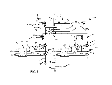
[0057] According to various embodiments, and referring to Figures 3 and 4, the
signal generator
145 may generate one or more stimulus signals. The stimulus signal may be
applied to the
electrodes, where two electrodes electrically couple to form a current path
through the target.
14
CA 03215315 2023- 10- 12
WO 2022/221504
PCT/US2022/024769
The present embodiments of the signal generator 145 may provide a stimulus
signal having 500
volts to 2000 volts. In various embodiments, the signal generator 145 may
comprise a current
source circuit 300, a plurality of driver circuits, and a current sense
circuit 315. The plurality of
driver circuits may be connected to the current source circuit 300 at a first
node Ni and
connected to the current sense circuit at a second node N2. The second node N2
may electrically
connect the plurality of driver circuits directly to a ground or to the ground
via a passive element,
such a resistor.
[0058] The current source circuit 300 may be configured to provide a constant
current to the
plurality of driver circuits. In various embodiments, the current source
circuit 300 may comprise
a high-side driver module 325 responsive to a control signal CC DRIVE, a
regulator 340, and a
seventh switch device S7. The current source circuit 300 may be connected to
receive a stimulus
supply voltage Vs, such as a 1000V power supply, a power supply voltage, and a
bias voltage
VB , such as an 18V bias supply. For example, the current source circuit 300
may further
comprise a first terminal 350 to receive the stimulus supply voltage Vs and a
second terminal
355 to receive the bias voltage VB .
100591 In some embodiments, the current source circuit 300 may further
comprise a transformer
320 connected to the power supply voltage and the high-side driver module 325
(for example, as
illustrated in Figure 3). The transformer 320 may comprise a primary winding
and one or more
secondary windings. The primary winding of the transformer 320 may be
connected to a power
supply (e.g., a battery) at a battery terminal 345 and thus operate according
to current provided
by the power supply. The transformer 320 may also be responsive to a control
signal
BOOST PWM that is capable of modulating or otherwise varying the current
through the
primary winding. For example, a fifth switch device S5, configured to be
controlled by the
control signal BOOST PWM, may be connected to the primary winding. In
embodiments, the
current source circuit 300 may be configured to generate one or more voltages.
For example, the
current source circuit 300 may comprise a transformer (e.g., transformer 320)
configured to
generate the stimulus supply voltage Vs and the bias voltage VB according to
power received
from a power supply at the battery terminal 345.
[0060] The high-side driver module 325 may be used in conjunction with the
regulator 340 and
the seventh switch device S7 to generate the constant current. The high-side
driver module 325
may be responsive to and operate according to the control signal CC DRIVE and
the bias
CA 03215315 2023- 10- 12
WO 2022/221504
PCT/US2022/024769
voltage VB . In various embodiments, the high-side driver module 325 may
comprise any circuit
or system suitable for driving a gate of an electronic switching device,
providing voltage
isolation and/or impedance matching. For example, the high-side driver module
325 may
comprise an optocoupler circuit to receive the control signal CC DRIVE and
transfer electrical
signals between two isolated circuits by using light, a gate-drive
transformer, or the like.
[0061] The regulator 340 may be used in conjunction with the high-side driver
module 325 and
the seventh switch device S7 to generate the constant current. In various
embodiments, the
regulator 340 may comprise any circuit or system suitable for regulating a
voltage and/or current
and monitoring voltage, and the regulator 340 may provide an adjustable output
voltage. In an
exemplary embodiment, the regulator 340 may comprise a first terminal A, a
second terminal K,
and a third terminal REF. The first terminal A may be connected to the first
node Ni, the
second terminal K may be connected to an output terminal of the high-side
driver module 325,
and the third terminal may be connected to a ground common with the high-side
driver module
325.
100621 The seventh switch device S7 may be used in conjunction with the high-
side driver
module 325 and the regulator 340 to generate the constant current. The seventh
switch device S7
may comprise any device or circuit suitable for controlling current flow, such
as a transistor
(e.g., a metal-oxide-semiconductor filed-effect transistor (MOSFET) or an
insulated gate bipolar
transistor (IGBT)) or a silicon controlled rectifier, and having a first
terminal, a second terminal,
and a third terminal. In an exemplary embodiment, the first terminal of the
seventh switch
device S7 may be connected to receive the stimulus supply voltage Vs via the
first terminal 350
of the current source circuit 300.
100631 The current source circuit 300 may further comprise any number of
passive elements,
such as resistive elements (e.g., a third resistor R3 and a fourth resistor
R4), charge storage
devices (e.g., a third capacitor C3 and a fourth capacitor C4), and diodes
(e.g., a third diode D3
and a fourth diode D4). The current source circuit 300 may further comprise
any number of
switch devices (e.g., the fifth switch device S5 and a sixth switch device
S6). The switch devices
may be a current controlled device or a voltage controlled device and may
comprise any device
or circuit suitable for controlling current flow, such as a transistor (for
example, an IGBT as
illustrated in Figure 3), a silicon controlled rectifier (for example, as
illustrated in Figure 4), a
MOSFET, or the like.
16
CA 03215315 2023- 10- 12
WO 2022/221504
PCT/US2022/024769
[0064] In various embodiments, the sixth switch device S6 may be connected to
a terminal of the
high-side driver module 325 and may be configured to receive and operate
according to the
control signal CC DRIVE. For example, the control signal CC DRIVE may be used
turn the
sixth switch device S6 ON and OFF. The high-side driver module 325 may be
responsive to
and operate according to the state of the sixth switch device S6. For example,
the high-side
driver module 325 may be activated (enabled) when the sixth switch device S6
is ON (enabled).
[0065] In one embodiment, and referring to Figure 4, the current source
circuit 300 may further
comprise a stabilizer element (not shown) connected in parallel with the third
resistor R3. The
stabilizer element may be used to more precisely control the waveform of the
current output by
the current source circuit 300. For example, the stabilizer element may
comprise a capacitor.
[0066] In an exemplary embodiment, the signal generator 145 may comprise a
first driver circuit
305 and a second driver circuit 310 connected to the current source circuit
300 at the first node
Ni. Accordingly, all of the driver circuits may be operated by the current
source circuit 300. In
other embodiments, the signal generator 145 may comprise any number of driver
circuits, such
as ten (10) driver circuits. According to various embodiments, each driver
circuit may generate
and provide the stimulus signal to a single electrode.
[0067] The first driver circuit 305 may be configured to generate a first
stimulus signal and
transmit the first stimulus signal to an electrode (e.g., the first electrode
El) via a first driver
terminal HV1. The first driver circuit 305 may comprise a first driver module
330, a first charge
storage circuit, a first switch device Si, and a second switch device S2.
[0068] The first driver module 330 may be configured to receive enable signals
from the
processing circuit 135 and control the operation of the first driver circuit
305 via the enable
signals. For example, the first driver module 305 may receive a first high
enable signal HEN1
and a first low enable signal LEN1 from the processing circuit 135 at inputs
INA and INB,
respectively, and transmit the enable signals to outputs OUTA and OUTB. The
first high enable
signal HEN1 and the first low enable signal LEN1 may control the first and
second switch
devices Si, S2.
[0069] In embodiments, the first driver module 330 may be further configured
to receive a bias
voltage VB. Transmitting the enable signals to outputs OUTA and OUTB may
comprise
providing (e.g., modifying, adjusting, determining, etc.) a voltage of the
enable signals relative to
the bias voltage Vs. A voltage of one or more of the enable signals at outputs
OUTA and/or
17
CA 03215315 2023- 10- 12
WO 2022/221504
PCT/US2022/024769
OUTB may be greater than a voltage of the one or more respective enable
signals received at
inputs INA and/or INB. For example, the first high enable signal HEN1 input
via input INA and
the first low enable signal LEN1 input via input INB may each have a reference
voltage (e.g., 5
volts). According to the received enable signals and the bias voltage VB, the
first driver module
330 may be configured to provide (e.g., generate, modify, transform, etc.)
enable signals with a
voltage equal to the bias voltage bias voltage Vs. For example, the first high
enable signal HEN1
output via output OUTA may have a voltage equal to the bias voltage Vs and the
first low enable
signal LEN1 output via output OUTB may have a voltage equal to the bias
voltage VB In
embodiments, providing the enable signals via outputs OUTA and OUTB may be
performed
using voltages separately available within CEW 100 and/or without a separate
transformer
included in the first driver module 330.
100701 The first switch device Si may operate according to the current source
circuit 300 and
operate in conjunction with the second switch device S2 and the first driver
module 330 to
control the stimulus signal at the first driver terminal HV1. In various
embodiments, the first
switch device Si may comprise any circuit and/or device suitable for
controlling a current and/or
voltage at the first driver terminal HV1. In various embodiments, the first
switch device Si may
comprise three terminals, such as a positive terminal, a negative terminal,
and a gate terminal.
For example, the first switch device Si may comprise a transistor, such as a
metal-oxide-
semiconductor filed-effect transistor, an insulated gate bipolar transistor, a
silicon controlled
rectifier, or the like. In an exemplary embodiment, the first switch device Si
may be connected
to the first node Ni via its positive terminal. The negative terminal of the
first switch device Si
may be connected to the first charge storage device Cl. The gate terminal of
the first switch
device Si may be connected to the first driver module 330 and receive the
first high enable
signal HEN1 via output OUTA
100711 The second switch device S2 may operate according to the first driver
module 330 and in
conjunction with the first switch device Si to control the stimulus signal at
the first driver
terminal HV1. In various embodiments, the second switch device S2 may comprise
any circuit
and/or device suitable for controlling a current and/or voltage at the first
driver terminal HV1. In
various embodiments, the second switch device S2 may comprise three terminals,
such as a
positive terminal, a negative terminal, and a gate terminal. For example, the
second switch
device S2 may comprise a transistor, such as a metal-oxide-semiconductor filed-
effect transistor,
18
CA 03215315 2023- 10- 12
WO 2022/221504
PCT/US2022/024769
a silicon controlled rectifier, or the like. In an exemplary embodiment, the
second switch device
S2 may be connected to the second node N2 via its negative terminal. The
positive terminal of
the second switch device S2 may be connected to the negative terminal of the
first switch device
Si at a third node N3. In other words, the first and second switch devices Si,
S2 may be
connected in series with each other at the third node N3. The gate terminal of
the second switch
device S2 may be connected to the first driver module 330 and receive the
first low enable signal
LEN1 via output OUTB. Accordingly, the first switch device Si and the second
switch device
S2 may be operated independent from each other.
100721 In various embodiments, controlling the first switch device Si to be
disposed in a closed
state (e.g., turned ON) may require a minimum voltage difference (e.g.,
voltage drop) to be
maintained between a control terminal (e.g., gate terminal) and an output
terminal (e.g., negative
terminal) of the first switch device Si. For example, and in accordance with a
stimulus signal
and resistance of a target, a higher voltage of at least 10 volts, between 10
volts and 20 volts, or
at least 20 volts may be required at the control terminal relative to the
output terminal in order to
drive the first switch device Si in the closed state. When this voltage
difference is not provided,
the first switch device Si may be driven in a closed state (e.g., turned OFF).
In embodiments,
the higher voltage may be provided by a transformer and other passive elements
separately
coupled to the first switch device Si. For example, a control signal may be
provided to the
control terminal of the first switch device Si by a set of electrical circuit
devices similar to the
transformer 320, the third capacitor C3, and the fourth diode D4 coupled to a
control terminal of
the seventh switch device S7. However, an additional transformer and other
such electrical
circuit devices may require additional space in housing 110 of the CEW 100,
increasing a
minimum required size of the housing 110. The additional space required may be
particularly
sizeable when these additional electrical circuit devices are separately
provided for each driver
circuit of a plurality of driver circuits in the CEW 100. The additional
electrical circuit devices
may also increase an overall complexity of electrically integrating and
insulating each driver
circuit of the plurality of driver circuits of the CEW 100.
100731 Embodiments according to various aspects of the present disclosure
address these issues
and others by using a charge storage circuit for each driver circuit. For
example, the first driver
circuit 305 may comprise a first charge storage circuit 360 and the second
driver circuit 310 may
comprise a second charge storage circuit 365. Each charge storage circuit
360,365 may comprise
19
CA 03215315 2023- 10- 12
WO 2022/221504
PCT/US2022/024769
a plurality of passive electrical circuit devices. Each charge storage circuit
360,365 may
comprise a reduced set of electrical circuit devices. For example, and in
contrast with the
electrical circuit devices coupled to the seventh switch device S7 in Figure
3, each of the first
charge storage circuit 360 and the second charge storage circuit 365 may
exclude a transformer.
Each charge storage circuit 360,365 may be electrically coupled between a
power source and a
respective switch device. For example, the first charge storage circuit 360
may be coupled
between the first driver module 330 and the first switch device Si, while the
second charge
storage circuit 365 may be coupled between a second driver module 335 and a
third switch
device S3. Each charge storage circuit 360,365 may be connected in parallel
with at least a
portion of the respective switch device. For example, the first charge storage
circuit 360 may be
coupled between a control terminal of the first switch device Si and an output
terminal of the
first switch device Si. The second charge storage circuit 365 may be coupled
between a control
terminal of the third switch device S3 and an output terminal of the third
switch device S3.
100741 The first charge storage circuit 365 may be configured to control the
first switch device
Si. Control of the first switch device Si may comprise providing a charge to a
control terminal
of the first switch device Si. The charge may be provided to the control
terminal to drive the
first switch device Si in a closed state. The first charge storage circuit 360
may be electrically
connected in parallel with the control terminal of the first switch device Si
and an output
terminal of the first switch device Si such that the charge may provide a
higher voltage at the
control terminal relative to the output terminal. The higher voltage may be
provided independent
of changes (e.g., increases, decreases, etc.) in a voltage provided at the
output terminal of the
first switch device Si. In embodiments, the first charge storage circuit 360
may be a
transformerless charge storage circuit, comprise one or more capacitors,
and/or comprise one or
more resistive elements. For example, the first charge storage circuit 360 may
comprise a first
charge storage device Cl and a first resistor Rl. The first charge storage
device Cl may be
connected between the gate terminal of the first switch device S1 and the
third node N3. For
example, in a case where the first charge storage device Cl comprises a
capacitor, a first terminal
of the capacitor may be connected to the gate terminal of the first switch
device Si and a second
terminal of the capacitor may be connected to the third node N3. In
embodiments, the first
charge storage device Cl of the first charge storage circuit 360 may be
configured to store a
CA 03215315 2023- 10- 12
WO 2022/221504
PCT/US2022/024769
charge provided to the first charge storage circuit 360 according to the
enable signal output via
OUTA of the first driver module 330.
100751 The first charge storage circuit 360 may further comprise a resistive
element, such as
resistor R1, connected in parallel with the first charge storage device Cl.
The resistive element
may be configured to discharge a charge stored in the first charge storage
circuit 360. Values of
the first charge storage device Cl, resistive element, and/or other electrical
circuit devices of the
first charge storage circuit may be selected such that a minimum voltage is
maintained across the
control terminal and the output terminal of the first switch device Si for a
minimum period of
time after a charge is stored in the first charge storage circuit 360
according to the first high
enable signal HEM_.
100761 In addition, the first charge storage circuit 360 may comprise a first
diode D1 connected
between the first driver module 330 and the gate terminal of the first switch
device Si. The first
diode D1 may be coupled to a first terminal of the first charge storage
circuit 360. For example,
the first diode D1 may be coupled to a first terminal of the first charge
storage device Cl.
100771 In one embodiment, and referring to Figure 4, the first charge storage
circuit 360 may
further comprise a tenth resistor R10 connected between the first storage
device Cl and the first
switch device Si. Accordingly, the first terminal of the first charge storage
circuit 360 may be
further coupled to the control terminal of the first switch device Si directly
or indirectly via a
resistive element, such as the tenth resistor R10.
100781 In addition, and referring to Figure 4, the first driver circuit 305
may further comprise an
eleventh resistor R11 connected between the second switch device S2 and the
first driver module
330, and a twelfth resistor R12 connecting the eleventh resistor R11 to the
second node N2.
100791 The second driver circuit 310 may be configured to generate a second
stimulus signal and
transmit the second stimulus signal to an electrode (e.g., the second
electrode E2) via a second
driver terminal HV2. The second driver circuit 310 may comprise a second
driver module 335, a
second charge storage circuit 365, a third switch device S3, and a fourth
switch device S4.
100801 The second driver module 335 may be configured to receive enable
signals from the
processing circuit 135 and control the operation of the second driver circuit
310 via the enable
signals. For example, the second driver module 335 may receive a second high
enable signal
HEN2 and a second low enable signal LEN2 from the processing circuit 135 at
inputs INA and
INB, respectively, and transmit the enable signals to outputs OUTA and OUTB.
The second
21
CA 03215315 2023- 10- 12
WO 2022/221504
PCT/US2022/024769
high enable signal HEN2 and the second low enable signal LEN2 may control the
third and
fourth switch devices S3, S4.
100811 In embodiments, the second driver module 335 may be further configured
to receive a
bias voltage VB. Transmitting the enable signals to outputs OUTA and OUTB may
comprise
providing (e.g., modifying, adjusting, determining, etc.) a voltage of the
enable signals relative to
the bias voltage VB. A voltage of one or more of the enable signals at outputs
OUTA and/or
OUTB may be greater than a voltage of the one or more respective enable
signals received at
inputs INA and/or INB. For example, the first high enable signal HEN1 input
via input INA and
the first low enable signal LEN1 input via input INB may each have a reference
voltage (e.g., 5
volts). The second driver module 335 may be configured to provide (e.g.,
generate, modify,
transform, etc.) enable signals according to the received enable signals and
the bias voltage VB in
which the second high enable signal HEN2 output via output OUTA has a voltage
equal to the
bias voltage VB and the second low enable signal LEN2 output via output OUTB
has a voltage
equal to the bias voltage VB. In embodiments, providing the enable signals via
outputs OUTA
and OUTB may be performed using voltages separately available within the CEW
100 and/or
without using a separate transformer in the second driver module 335.
100821 The third switch device S3 may operate according to the current source
circuit 300 and
operate in conjunction with the fourth switch device S4 and the second driver
module 335 to
control the stimulus signal at the second driver terminal HV2. In various
embodiments, the third
switch device S3 may comprise any circuit and/or device suitable for
controlling a current and/or
voltage at the first driver terminal HV1. In various embodiments, the third
switch device S3 may
comprise three terminals, such as a positive terminal, a negative terminal,
and a gate terminal.
For example, the third switch device S3 may comprise a transistor, such as a
metal-oxide-
semiconductor filed-effect transistor, a silicon controlled rectifier, or the
like. In an exemplary
embodiment, the third switch device S3 may be connected to the first node Ni
via its positive
terminal. The negative terminal of the third switch device S3 may be connected
to the second
charge storage device C2. The gate terminal of the third switch device S3 may
be connected to
the second driver module 335 and receive the second high enable signal HEN2
via the second
driver module output OUTA.
100831 The fourth switch device S4 may operate according to the second driver
module 335 and
in conjunction with the third switch device S3 to control the stimulus signal
at the second driver
22
CA 03215315 2023- 10- 12
WO 2022/221504
PCT/US2022/024769
terminal HV2. In various embodiments, the second switch device S may comprise
any circuit
and/or device suitable for controlling a current and/or voltage at the first
driver terminal HV1. In
various embodiments, the fourth switch device S4 may comprise three terminals,
such as a
positive terminal, a negative terminal, and a gate terminal. For example, the
fourth switch device
S4 may comprise a transistor, such as a metal-oxide-semiconductor filed-effect
transistor, a
silicon controlled rectifier, or the like. In an exemplary embodiment, the
fourth switch device S4
may be connected to the second node N2 via its negative terminal. The positive
terminal of the
fourth switch device S4 may be connected to the negative terminal of the third
switch device S3
at a fourth node N4. In other words, the third and fourth switch devices S3,
S4 may be connected
in series with each other at the fourth node N4. The gate terminal of the
fourth switch device S4
may be connected to the second driver module 335 and receive the second low
enable signal
LEN2 via output OUTB. Accordingly, the third switch device S3 and the fourth
switch device
S4 may be operated independent from each other.
100841 The second charge storage circuit 365 may be configured to control
third switch device
S3. Control of the third switch device S3 may comprise providing a charge to a
control terminal
of the third switch device S3. The charge may be provided to the control
terminal to drive the
third switch device S3 in a closed state. The second charge storage circuit
365 may be
electrically connected in parallel with the control terminal of the third
switch device S3 and an
output terminal of the third switch device S3 such that the charge may provide
a higher voltage
at the control terminal relative to the output terminal. The higher voltage
may be provided
independent of changes (e.g., increases, decreases, etc.) in a voltage provide
at the output
terminal of the third switch device S3. In embodiments, the second charge
storage circuit 365
may be a transformerless charge storage circuit, comprise one or more
capacitors, and/or
comprise one or more resistive elements. For example, the second charge
storage circuit 365
may comprise a second charge storage device C2 and a second resistor R2.
100851 The second charge storage device C2 may be connected between the gate
terminal of the
third switch device S3 and the fourth node N4. For example, in the case where
the second
charge storage device C2 comprises a capacitor, a first terminal of the
capacitor may be
connected to the gate terminal of the third switch device S3 and a second
terminal of the
capacitor may be connected to the fourth node N4. In embodiments, the second
charge storage
device C2 of the second charge storage circuit 365 may be configured to store
a charge provided
23
CA 03215315 2023- 10- 12
WO 2022/221504
PCT/US2022/024769
to the second charge storage circuit 365 according to the enable signal output
via OUTA of the
second driver module 335.
100861 The second charge storage circuit 365 may further comprise a resistive
element, such as
resistor R2, connected in parallel with the second charge storage device C2.
The resistive
element may be configured to discharge a charge stored in the second charge
storage circuit 365.
Values of the second charge storage device C2, resistive element, and/or other
electrical circuit
devices of the second charge storage circuit 365 may be selected such that a
minimum voltage is
maintained across the control terminal and output terminal of the third switch
device S3 for a
minimum period of time after a charge according to the second high enable
signal HEN2 output
via output OUTA of the second driver module 335 is stored by the second charge
storage circuit
365. In embodiments, values of the electrical circuit devices of the second
charge storage circuit
365 (e.g., second charge storage device C2) may be equal to values of
corresponding electrical
circuit devices of the first charge storage circuit 360.
100871 In addition, the second charge storage circuit 365 may comprise a
second diode D2
connected between the second driver module 335 and the gate terminal of the
third switch device
S3. The second diode D2 may be coupled to a first terminal of the second
charge storage circuit
365. For example, the second diode D2 may be coupled to a first terminal of
the second charge
storage device C2.
100881 In one embodiment, and referring to Figure 4, the second charge storage
circuit 365 may
further comprise a thirteenth resistor R13 connected between the second
storage device C2 and
the third switch device S3. The first terminal of the second charge storage
circuit 365 may be
further coupled to a control terminal of the second switch device Si directly
or indirectly via a
resistive element such as the thirteenth resistor R13.
100891 In addition, and referring to Figure 4, the second driver circuit 305
may further comprise
a fourteenth resistor R14 connected between the fourth switch device S4 and
the second driver
module 335, and a fifteenth resistor R15 connecting the fourteenth resistor
R14 to the second
node N2.
100901 The current sense circuit 315 may be configured to measure a current
through a load,
such as the human target, and generate a sense signal SNS representing the
current through the
load. The current sense circuit 315 may transmit the sense signal SNS to the
processing circuit
135, wherein the processing circuit 135 may use the information provided by
the sense signal
24
CA 03215315 2023- 10- 12
WO 2022/221504
PCT/US2022/024769
SNS to adjust the charge output to the load. In various embodiments, the
current sense circuit
315 may comprise various passive elements, such as a sixth resistor R6, a
seventh resistor R7 an
eighth resistor R8, a ninth capacitor R9, and a fifth capacitor C5. The sixth
and seventh resistors
R6, R7 may be connected in series with each other and connected to a ground,
while the eighth
resistor R8 and the fifth capacitor C5 may be connected in parallel with the
sixth and seventh
resistors R6, R7 and connected to the ground. The sixth and ninth resistors
R6, R9 may be
directly connected to the second node N2. Accordingly, the sixth, seventh, and
ninth resistors
R6, R7, R9 connect the first and second driver circuits 305, 310 to the
ground.
[0091] According to various embodiments, the resistance value of the resistors
and the
capacitance of the capacitors (i.e., charge storage devices) may vary and may
be selected
according to the particular application, desired output current and/or output
voltage, desired
operating specifications, the value of the supply voltage and the bias
voltage, and the like.
[0092] In embodiments, switch devices of a driver circuit may comprise a same
type of switch
device. For example, in one embodiment, each of the first, second, third and
fourth switch
devices Si, S2, S3, S4 comprise a transistor, such as an IGBT or a MOSFET. In
another
embodiment, the first, second, third and fourth switch devices Sl, S2, S3, S4
may comprise a
silicon controlled rectifier. In other embodiments, switch devices of a driver
circuit may
comprise different types of switch devices. For example, and in yet another
embodiment, the
first and third switch devices Si, S3 may comprise a transistor, such as an
IGBT or a MOSFET,
and the second and fourth switch devices S2, S4 may comprise a silicon
controlled rectifier.
[0093] According to various embodiments, and referring to Figures 1-7, the CEW
100 may
perform electrical connectivity testing to determine which electrodes, if any,
made contact with
the target and are suitable for providing the stimulus signal. The CEW 100 may
provide the
stimulus signal to the target by operating the current source circuit 300 and
at least two driver
circuits that are determined to be in contact with the target.
[0094] According to various embodiments and with reference to Figure 6, the
CEW 100 is
depicted after deploying at least five electrodes (e.g., electrodes El, E2,
E5, E6 and E10). As
depicted, electrodes El, E2, E3, El are coupled to the target 5, and
electrode E5 is not coupled
to target 5 (e.g., a missed deployment). An electrode not coupled to a target
is unable to provide
a stimulus signal through the target. Testing electrical connectivity of
launched electrodes may
allow the CEW 100 to determine a state of connection of each electrode and
determine whether
CA 03215315 2023- 10- 12
WO 2022/221504
PCT/US2022/024769
each electrode is able to provide a stimulus signal through the target.
Testing electrical
connectivity of launched electrodes may also allow the CEW 100 to determine a
relative distance
between electrodes coupled to the target (e.g., dart spread, electrode spread,
etc.). A greater
distance between electrodes providing the stimulus signal may increase the
likelihood of
inducing NMI on the target.
[0095] The CEW 100 (e.g., via a signal generator) may be configured to apply
test signals on
launched electrodes to test the electrical connectivity of the electrode. For
example, the CEW
100 may apply a first test signal (e.g., a first voltage) on a first electrode
and a second test signal
(e.g., a second voltage) on a second electrode. The first test signal may
comprise a first voltage
and the second test signal may comprise a second voltage different from the
first voltage. The
first voltage may be greater than the second voltage.
[0096] The CEW 100 may detect a measurement voltage of each of the remaining
electrodes to
determine the state of connection of each of the remaining electrodes (wherein
each of the
remaining electrodes is not provided a test signal). The measurement voltage
may inform the
state of connection, as discussed further herein. For example, because each of
the remaining
electrodes coupled to the same target share electrical coupling with the first
electrode (provided
the first test signal) and/or the second electrode (provided the second test
signal), the
measurement voltage of a remaining electrode coupled to the target should be
greater than 0
volts (e.g., a same voltage as the first test signal, a same voltage as the
second test signal, a
voltage between the first test signal and the second test signal, etc.).
Because each of the
remaining electrodes not coupled to the same target do not share electrical
coupling with the first
electrode (provided the first test signal) and the second electrode (provided
the second test
signal), the measurement voltage of a remaining electrode not coupled to the
same target should
be 0 volts (or close to 0 volts).
[0097] The CEW 100 may determine a state of connection based on the
measurement voltage.
For example, in response to the measurement voltage being 0 volts, the state
of connection of the
third electrode is not connected" (or a representation of not connected)
(e.g., the third electrode
is not coupled to the target). In response to the measurement voltage being a
value equal to the
first voltage, equal to the second voltage, or between the first voltage and
the second voltage, the
state of connection of the third electrode is "connected" (or a representation
of connected) (e.g.,
the third electrode is coupled to the target). In response to the measurement
voltage being a value
26
CA 03215315 2023- 10- 12
WO 2022/221504
PCT/US2022/024769
numerically closer to the first voltage than the second voltage, the third
electrode may be coupled
to the target at a location on the target closer to the first electrode than
the second electrode (e.g.,
the first electrode is coupled at a first location, the second electrode is
coupled at a second
location, the third electrode is coupled at a third location, and the third
location is closer to the
first location than the second location). In response to the measurement
voltage being a value
numerically closer to the second voltage than the first voltage, the third
electrode may be coupled
to the target at a location on the target closer to the second electrode than
the first electrode (e.g.,
the first electrode is coupled at a first location, the second electrode is
coupled at a second
location, the third electrode is coupled at a third location, and the third
location is closer to the
second location than the first location). In response to the measurement
voltage being a value
that is the same (or about the same) as the first voltage, the state of
connection of the second
electrode is not connected" (or a representation of not connected) (e.g., the
first electrode and
the third electrode are coupled to the target, but the second electrode is not
coupled to the target).
In response to the measurement voltage being a value that is the same (or
about the same) as the
second voltage, the state of connection of the first electrode is not
connected" (or a
representation of not connected) (e.g., the second electrode and the third
electrode are coupled to
the target, but the first electrode is not coupled to the target).
[0098] In various embodiments, the CEW 100 may detect respective measurement
voltages at
multiple remaining electrodes at a same time. For example, the CEW 100 may
deploy at least
three electrodes towards a target. The CEW 100 may apply a first voltage of a
test signal to a
first electrode of the at least three electrodes and a second voltage of a
second test signal to a
second electrode of the at least three electrodes. The first voltage may be
greater than the second
voltage. The first voltage may be applied across the different first and
second electrodes at a
same time. In accordance with the test signals, the CEW 100 may concurrently
detect a first
measurement voltage at a third electrode from the at least three electrodes
and a second
measurement voltage at a fourth electrode from the at least four electrodes.
Accordingly, a
plurality of measurement voltages may be determined for a plurality of
electrodes in accordance
with a same one or more test signals (e.g., same test signal or pair of test
signals, etc.).
[0099] The CEW 100 may determine an electrode spread between electrodes based
on the state
of connection and/or the measurement voltage. For example, and as previously
discussed, in
response to the measurement voltage being a value numerically closer to the
first voltage than
27
CA 03215315 2023- 10- 12
WO 2022/221504
PCT/US2022/024769
the second voltage, the third electrode may be coupled to the target at a
location on the target
closer to the first electrode than the second electrode (e.g., the first
electrode is coupled at a first
location, the second electrode is coupled at a second location, the third
electrode is coupled at a
third location, and the third location is closer to the first location than
the second location).
Because the third electrode is closer to the first electrode than the second
electrode, a relative
electrode spread between the three electrodes can be determined (e.g., a first
electrode spread
between the first electrode and the second electrode is greater than a second
electrode spread
between the first electrode and the third electrode). As can be extrapolated
by one skilled in the
art, additional tests, measurement voltages, and states of connection may
further determine and
refine locations of the electrodes on the target, and the relative electrode
spread between
electrodes on the target.
101001 As discussed, the first voltage and the second voltage applied as test
signals may
comprise different values. For example, the first voltage may be greater than
the second voltage,
or the second voltage may be greater than the first voltage. The first voltage
and the second
voltage may each comprise low voltages. The first voltage and the second
voltage may each be
less than 50 volts. For example, the first voltage (or the second voltage) may
be less than 5 volts
and the second voltage (or the first voltage) may be greater than 10 volts. In
some embodiments,
the first voltage (or the second voltage) may be 3 volts and the second
voltage (or the first
voltage) may be 12 volts. In embodiments, a voltage difference between the
first voltage and the
second voltage may be one or more of less than ten volts, less than twenty
volts, less than thirty
volts, less than fifty volts, or less than one hundred volts. The voltage
difference may comprise a
difference of an absolute value of the first voltage and an absolute value of
the second voltage.
101011 In various embodiments, one or more measurement voltages and/or states
of connection
may be stored in memory of the CEW 100 by the processing circuit 135. Storing
the one or more
measurement voltages and/or the states of connection in memory may allow the
CEW 100 to
further use the collected data for reporting, testing, or other processes or
uses.
101021 In various embodiments, the CEW 100 may perform tests by applying test
signals in any
desired or structured order, and may perform as many tests as desired or
necessary to test each
launched electrode.
101031 In various embodiments, the CEW 100 may perform tests between pulses of
a stimulus
signal, between deployment of additional electrodes, and/or at any other time
as desired. For
28
CA 03215315 2023- 10- 12
WO 2022/221504
PCT/US2022/024769
example, the CEW 100 may apply a first test signal and a second test signal to
determine a first
state of connection of launched electrodes (e.g., as previously discussed).
After applying the first
test signal and the second test signal, the CEW 100 may provide a first pulse
of a stimulus signal
through a first pair of launched electrodes. The CEW 100 may then apply a
third test signal and a
fourth test signal to determine a second state of connection of launched
electrodes (e.g., as
previously discussed). After applying the third test signal and the fourth
test signal, the CEW 100
may provide a second pulse of the stimulus signal through a second pair of
launched electrodes.
The second pair of launched electrodes may be the same as the first pair of
launched electrodes.
The second pair of launched electrodes may be different from the first pair of
launched
electrodes (e.g., completely different, at least one electrode of the pair
different, etc.). The first
pair of launched electrodes may be based on the first state of connection
(e.g., the first pair may
include two electrodes coupled to the target, based on a determined electrode
spread, etc.). The
second pair of launched electrodes may be based on the second state of
connection and/or the
first state of connection (e.g., the first pair may include two electrodes
coupled to the target,
based on a determined electrode spread, etc.).
101041 The CEW 100 (e.g., via a signal generator 145) may be configured to
generate and apply
a stimulus signal to the target via the electrodes. In various embodiments,
the signal generator
145 may generate the stimulus signal at an output terminal of a driver circuit
that is associated
with an electrode that is determined to be in contact with the target. For
example, the CEW 100
may activate the first driver circuit 305 if the first electrode El is
determined to be in contact
with the target and generates the stimulus signal at the first driver terminal
HV1. The CEW 100
may also activate a receiving driver circuit associated with another electrode
that is determined
to be in contact with the target. For example, the CEW 100 may activate the
second driver circuit
310 if the second electrode E2 is determined to be in contact with the target.
It will be
understood that since each driver circuit comprises both a positive switch
device (e.g., the first
switch device Si of the first driver circuit 305 and the third switch device
S3 of the second driver
circuit 310) and a negative switch device (the second switch device S2 of the
first driver circuit
305 and the fourth switch device S4 of the second driver circuit 310), each
driver circuit may be
able to operate as the drive circuit and the receiving circuit.
101051 Embodiments of the present technology allow any pair of electrodes to
provide the
stimulus signal to the target. For example, the stimulus signal may be
delivered through the first
29
CA 03215315 2023- 10- 12
WO 2022/221504
PCT/US2022/024769
electrode El and the second electrode E2 via a first electrical connection
705, the stimulus signal
may be delivered through the first electrode El and the third electrode E3 via
a second electrical
connection 710, the stimulus signal may be delivered through the first
electrode El and the
fourth electrode E4 via a third electrical connection 730. Likewise, other
electrode pairs may
provide additional electrical connections, such as a fourth electrical
connection 720, a fifth
electrical connection 715, and a sixth electrical connection 725.
[0106] Generating the stimulus signal at the first driver terminal HV1
comprises charging the
first charge storage circuit 360 of the first driver circuit 305 and
selectively turning ON the first
switch device Si according to a charge of the first charge storage circuit
360. For example,
generating the stimulus signal may comprise charging the first charge storage
device Cl of the
first driver circuit 305 and selectively turning ON the first switch device Si
according to a
charge of the first charge storage device Cl. Charging the first charge
storage circuit 360 and
turning ON the first switch device S1 may comprise enabling the first high
enable signal HEN1
and the first low enable signal LEN1 substantially simultaneously at a first
time to. For example,
the processing circuit 135 may enable the first high enable signal HEN1 and
the first low enable
signal LEN1. When the first high enable signal HEN1 and the first low enable
signal LEN1 are
enabled, the first driver module 330 may provide the enabled signals via
outputs OUTA and
output OUTB. In accordance with the first low enable signal LEN1, the second
switch device S2
may be driven from an open state to a closed state (e.g., turned ON). When
second switch device
S2 is driven in the closed state, the third node N3 may be electrically
coupled to second node N2
The third node N3 may be further electrically coupled to ground via ninth
resistor R9.
Accordingly, a voltage of substantially zero volts may be coupled to the third
node N3 via the
second switch device S2 in the closed state.
[0107] In accordance with the first high enable signal HEN1, the first switch
device Si is driven
from an open state to a closed state (e.g., turned ON). The first high enable
signal HEN1 may
drive the first switch device S1 in the closed state for a period of time
starting at the first time to.
When the first switch device S1 is driven in the closed state, the first node
N1 may be electrically
coupled to the third node N3. At the first time to, the current source circuit
300 may be disabled
such that a stimulus signal from the current source circuit 300 is not
provided to the first node
Nl. For example, the current source circuit 300 may be disabled according to a
control signal
selectively provided to the seventh switch device S7. However, because of the
voltage
CA 03215315 2023- 10- 12
WO 2022/221504
PCT/US2022/024769
difference between the first high enable signal HEN2 and the third node N3 at
the first time to, a
charge may be stored by the first charge storage circuit. For example, the
charge may be stored
in charge storage device Cl. Providing the first high enable signal HEN1 via
output OUTA of
the first driver module 330 may comprise providing the first high enable
signal HEN1 to the first
charge storage circuit. The charge may be stored in the first charge storage
circuit according to
the first high enable signal HEN1.
[0108] Generating the stimulus signal at the first driver terminal HV1 may
further comprise
turning OFF the second switch device S2 after the first charge storage circuit
360 has been
charged at a second time ti. For example, the processing circuit 135 may
disable the first low
enable signal LEN1 at the second time ti after the first charge storage device
Cl has been
charged. The charge according to the first high enable signal HEN1 may be
stored in the first
charge storage circuit for a period of time between the first time to and the
second time ti. The
current source circuit 300 may remain disabled at the second time ti such that
a stimulus signal is
not provided to the first node Ni at the second time ti.
101091 Generating the stimulus signal at the first driver terminal HV1 may
further comprise
turning OFF the first switch device Si after the first charge storage circuit
360 has been charged
at the second time ti. For example, the processing circuit 135 may disable the
first high enable
signal HEN1 at the second time ti. Disabling the first high enable signal HEN1
may disable the
first high enable signal HEN1 provided via output OUTA. When the first high
enable signal
HEN1 is disabled at the second time ti, a charge operable to maintain the
first switch device Si in
the closed state may be stored in the first charge storage circuit. For
example, the charge stored
in the first charge storage device Cl prior to the second time ti may be
maintained at a control
terminal of the first switch device Si. The first charge storage circuit 360
of the first driver 305
may prevent current from flowing into the first driver module 330 when the
first high enable
signal HEN1 is disabled. For example, the first diode D1 may prevent current
from flowing into
the first driver module 330. However, after the first high enable signal HEN1
is disabled, a
charge may be maintained at a control terminal of the first switch device Si
by the first charge
storage circuit 360 such that the first switch device Si may remain in a
closed state and the first
node Ni may be coupled to the third node N3. Electrical circuit devices of the
first charge
storage circuit 360, such as first charge storage device Cl and first resistor
R1, may be
configured such that a minimum charge for retaining the first switch device Si
in the closed state
31
CA 03215315 2023- 10- 12
WO 2022/221504
PCT/US2022/024769
may be maintained after the first high enable signal HEN1 is disabled. At the
second time ti,
charge may begin to discharge via one or more resistive elements (e.g., the
first resistor R1),
while remaining greater than the minimum charge.
101101 Generating the stimulus signal may further comprise turning ON the
fourth switch device
S4 at a third time t2. For example, the processing circuit 135 may enable the
second low enable
signal LEN2 at the third time t2. When the second low enable signal LEN2 is
enabled, the
second driver module 335 may provide the second low enable signal LEN2 from
output OUTB
of the second driver module 335. The fourth switch device S4 is driven from an
open state into a
closed state in accordance with second low enable signal LEN2. When the fourth
switch device
S4 is driven in the closed state, the fourth node N4 may be electrically
coupled to the second
node N2. The fourth node N4 may be further electrically coupled to ground via
the ninth resistor
R9. Accordingly, a voltage of substantially zero volts may be coupled to the
fourth node N4 via
the fourth switch device S4 in the closed state.
101111 After a delay, and at a fourth time t3, the processing circuit 135 may
turn ON the current
source circuit 300 by enabling the control signal CC DRIVE (illustrated as
"CC" in Figure 5).
The control signal CC DRIVE may be provided to the seventh switch device S7 to
enable the
current source circuit 300 at the fourth time t3. At the fourth time t3,
current will flow from the
current source circuit 300 through a current path comprising the first switch
device Si, the first
driver terminal HV1, the first electrode El (which is associated with the
first driver circuit 305),
the load (target), the second electrode E2 (which is associated with the
second driver circuit
310), the second driver terminal HV2, the fourth switch device S4, the ninth
resistor R9, and to
the ground. At the fourth time t3, the fourth switch device S4 may have a
polarity opposite a
polarity of a first switch device Si. For example, the fourth switch device S4
may have a
negative polarity comprising a voltage potential of approximately zero volts,
and the first switch
device Si may have a positive polarity comprising a voltage potential of
approximately 1000
volts. In embodiments, a voltage potential of a switch device may comprise a
voltage potential
coupled across the switch device and/or provided at a cathode of the switch
device. In
accordance with the opposite polarities, the current of the stimulus signal
may be delivered to the
load via the first switch device Si and the fourth switch device S4.
101121 At the fourth time t3, the first switch device Si may remain in a
closed state according to
a charge provided by the first charge storage circuit 360. For example, a
charge stored by the
32
CA 03215315 2023- 10- 12
WO 2022/221504
PCT/US2022/024769
first charge storage device Cl may remain above a minimum voltage required to
drive the first
switch device Si in the closed state at the fourth time t3. Between the second
time ti and the
fourth time t3, current may flow across a resistive element (e.g., first
resistor R1) of the first
charge storage circuit 360, decreasing the charge provided to the control
terminal of the first
switch device SI. Accordingly, the charge provided by the first charge storage
circuit 360 at the
fourth time t3 may be less that the charge provided to the first switch device
S1 at the second
time ti However, the decreased charge may remain greater than a minimum
voltage required to
dispose the first switch device Si in a closed state at the fourth time ti
101131 At a fifth time t4, the CEW 100 may turn OFF the current source circuit
300. For
example, the processing circuit 135 may disable the control signal CC DRIVE.
The processing
circuit 135 may disable the control signal CC DRIVE based on the actual,
measured current
detected by the current sense circuit 315 and the desired amount of charge
delivered to the target.
For instance, the desired charge may range from 4114.iC to 1001.(C. The
control signal CC DRIVE
may be enabled for a duration of 251..is to 120p. The first switch device Si
may continue to stay
ON for a period of time between the fourth time t3 and the fifth time t4. The
stimulus signal from
the current source circuit 300 may be provided via the first driver terminal
HV1 for the period of
time despite a lack of an enable signal being applied to the first driver
circuit 305 from
processing circuit 135 during the period of time. The first switch device Si
may be passively
driven during this period of time.
101141 After processing circuit 135 turns OFF the current source circuit 300,
and at a sixth time
t5, the processing circuit 135 may turn OFF the fourth switch device S4. The
first switch device
Si may continue to stay ON for a period of time between the fifth time t4 and
the sixth time t5.
The first switch device Si may continue to stay ON according to a charge
provided to the first
switch device Si by the first charge storage circuit 360 of the first driver
circuit 305. The first
switch device Si may continue to stay ON for a period of time after the sixth
time t5 until the
first charge storage circuit 360 is sufficiently discharged to turn OFF the
first switch device Si.
For example, first switch device Si may continue to stay ON for a period of
time after the sixth
time t5 until the first charge storage device Cl is sufficiently discharged to
dispose the first
switch device in an open state (e.g., turned off). The first switch device Si
may be on for a
duration of 30011s to 1000p. Accordingly, the first charge storage circuit 360
may be configured
to store the charge for a first period of time greater than a second period of
time in which the
33
CA 03215315 2023- 10- 12
WO 2022/221504
PCT/US2022/024769
current source circuit 300 generates a current flow path through the first
switch device Si, the
first terminal HV1, the load, and the second terminal HV2. Electrical circuit
devices of the first
charge storage circuit 360, such as at least one capacitor (e.g., first charge
storage device Cl) and
at least one resistor (e.g., R1) may be configured to store the charge for the
first period of time.
According to the charge stored in the first charge storage circuit 360, the
first switch device S I
may automatically turn OFF after the first period of time.
[0115] In embodiments, a second stimulus signal may be provided via the second
driver terminal
HV2 by switching the enable signals applied to the first driver circuit 305
and the second driver
circuit 310 from the processing circuit 135. For example, the second high and
low enable signals
REN2 and LEN2 may be simultaneously provided to the third switch device S3 and
the fourth
switch device S4, the second high and low enable signals HEN2 and LEN2 may
then be disabled
(e.g., terminated), and the first low enable signal LEN1 may then be provided
to the second
switch device S2. At this time, the current source circuit 300 may be enabled
such that current of
the second stimulus signal will flow from the current source circuit 300
through a current flow
path comprising the third switch device S3, the second driver terminal HV2,
the second electrode
E2 (which is associated with the second driver circuit 310), the load
(target), the first electrode
El (which is associated with the first driver circuit 305), the first driver
terminal HV1, the
second switch device S2, the ninth resistor R9, and to the ground.
Accordingly, a same switch
device (e.g., second switch device S2 or fourth switch device S4) may be used
to provide both a
first polarity of one pulse of a stimulus signal and a second, opposite
polarity of another,
different pulse of the stimulus signal. A same current source circuit 300 may
be configured to
provide each pulse of stimulus signal across different pairs of electrodes of
a plurality of
electrodes deployed from the CEW 100.
[0116] The foregoing description discusses implementations (e.g.,
embodiments), which may be
changed or modified without departing from the scope of the present disclosure
as defined in the
claims. Benefits, other advantages, and solutions to problems have been
described herein with
regard to specific embodiments. Furthermore, the connecting lines shown in the
various figures
contained herein are intended to represent exemplary functional relationships
and/or physical
couplings between the various elements. It should be noted that many
alternative or additional
functional relationships or physical connections may be present in a practical
system. However,
the benefits, advantages, solutions to problems, and any elements that may
cause any benefit,
34
CA 03215315 2023- 10- 12
WO 2022/221504
PCT/US2022/024769
advantage, or solution to occur or become more pronounced are not to be
construed as critical,
required, or essential features or elements of the disclosures. The scope of
the disclosure is
accordingly to be limited by nothing other than the appended claims and their
legal equivalents,
in which reference to an element in the singular is not intended to mean "one
and only one"
unless explicitly so stated, but rather "one or more." Moreover, where a
phrase similar to "at
least one of A, B, or C" is used in the claims, it is intended that the phrase
be interpreted to mean
that A alone may be present in an embodiment, B alone may be present in an
embodiment, C
alone may be present in an embodiment, or that any combination of the elements
A, B and C
may be present in a single embodiment; for example, A and B, A and C, B and C,
or A and B
and C.
101171 Systems, methods and apparatus are provided herein. In the detailed
description herein,
references to "various embodiments," "one embodiment," "an embodiment," "an
example
embodiment," etc., indicate that the embodiment described may include a
particular feature,
structure, or characteristic, but every embodiment may not necessarily include
the particular
feature, structure, or characteristic. Moreover, such phrases are not
necessarily referring to the
same embodiment. Further, when a particular feature, structure, or
characteristic is described in
connection with an embodiment, it is submitted that it is within the knowledge
of one skilled in
the art to affect such feature, structure, or characteristic in connection
with other embodiments
whether or not explicitly described. After reading the description, it will be
apparent to one
skilled in the relevant art(s) how to implement the disclosure in alternative
embodiments.
Furthermore, no element, component, or method step in the present disclosure
is intended to be
dedicated to the public regardless of whether the element, component, or
method step is
explicitly recited in the claims. No claim element is intended to invoke 35
U.S.C. 112(t) unless
the element is expressly recited using the phrase "means for." As used herein,
the terms
"comprises," "comprising," or any other variation thereof, are intended to
cover a non-exclusive
inclusion, such that a process, method, article, or apparatus that comprises a
list of elements does
not include only those elements but may include other elements not expressly
listed or inherent
to such process, method, article, or apparatus. In the specification and
claims, the words "a" and
"an." are used as indefinite articles meaning "one or more." While for the
sake of clarity of
description, several specific embodiments have been described, the scope of
the invention is
intended to be measured by the claims as set forth below.
CA 03215315 2023- 10- 12