Note : Les descriptions sont présentées dans la langue officielle dans laquelle elles ont été soumises.
1
DESCRIPTION
TITLE OF INVENTION:PIEZOELECTRIC ELEMENT AND PRODUCTION METHOD
THEREFOR
TECHNICAL FIELD
[0001]
The techniques disclosed by the present specification relate to a
piezoelectric
element and a method for producing a piezoelectric element.
BACKGROUND ART
[0002]
Hitherto, PZT (lead zirconate titanate) has been widely used as a ceramic
material
exhibiting piezoelectricity. However, PZT, containing a lead component, evokes
a problematic
impact on the environment, and thus demand has arisen for development of a
piezoelectric
ceramic containing no lead.
[0003]
Also, electronic parts employing a piezoelectric ceramic are generally
produced by
stacking ceramic green sheets that are to serve as piezoelectric ceramic
layers and electrically
conductive films that are to serve as electrodes, and co-firing the two
components. As an
electrode material, Pt, Ag-Pd alloy, and similar materials are widely used.
However, these
electrode materials are expensive and readily evoke migration. Thus, in recent
years, Ni (nickel)
has been proposed as an alternative material which is inexpensive and in which
migration is
suppressed. Since Ni readily undergoes oxidation when fired in air, such
firing must be
conducted in a reducing atmosphere. In the case where Ni is co-fired with a
piezoelectric
ceramic material, for example, a lead-containing zirconate titanate material
or a lead titanate
material, lead is chemically reduced in the atmosphere. In such a case, a
reliable piezoelectric
characteristic fails to be attained.
[0004]
In recent years' research in finding a lead-free piezoelectric ceramic
material which
contains no lead and which can exhibit piezoelectricity even after firing in a
reducing
CA 03218650 2023- 11- 9
2
atmosphere, there have been developed, as promising candidates, a variety of
lead-free
piezoelectric ceramic compositions containing an alkali niobate-based
perovskite oxide as a
primary phase (see, Patent Literatures 1 and 2).
CITATION LIST
PATENT LITERATURE
[0005]
Patent Literature 1: JP 5862983B
Patent Literature 2: JP 6489333B
SUMMARY OF INVENTION
TECHNICAL PROBLEM
[0006]
The aforementioned lead-free piezoelectric ceramic compositions exhibit a
dielectric loss (tano) of about 5%, and such a considerably large dielectric
loss may affect
characteristics including insulation performance. If such a ceramic
composition is subjected to
a polarization treatment including application of a strong electrical field at
a temperature of
some tens of degrees Celsius or to operation a device employing the
composition, leakage or
dielectric breakdown, as well as temperature elevation may readily occur.
SOLUTION TO PROBLEM
[0007]
The present specification discloses a piezoelectric element having a
piezoelectric
body and an electrode in contact with the piezoelectric body, the
piezoelectric body being
formed of a lead-free piezoelectric ceramic composition which includes a
primary phase formed
of an alkali niobate-based perovskite oxide represented by a compositional
formula
(Al aMlb)c(NbiliMnaTid3Zrd4Hfd5)03+e (wherein element Al represents at least
one species
among the alkali metals; element M1 represents at least one species among Ba,
Ca, and Sr;
the following conditions: 0<a<1, 0<b<1, a+b=1, 0.80<c<1.10, 0<dl<1, 0<d2<1,
0<d3<1,
1:114<1,015<1, and dl+d2+d3+d4+d5=1, are satisfied; and e represents a value
showing the
degree of deficiency or excess of oxygen) and which satisfies the condition:
b/(d3+d4+d51,
and the electrode containing a base metal as a main component.
[0008]
CA 03218650 2023- 11- 9
3
The present specification also discloses a method for producing a
piezoelectric
element, the method including: a calcination step of mixing raw materials of a
lead-free
piezoelectric ceramic composition which includes a primary phase formed of an
alkali niobate-
based perovskite oxide represented by a compositional formula
(AlaM1b)c(NbaiMnaTid3Zrd4Hfd5)03+e (wherein element Al represents at least one
species
among the alkali metals; element M1 represents at least one species among Ba,
Ca, and Sr;
the following conditions: 0<a<1, 0<b<1, a+b=1, 0.80<c<1.10, 0<dl<1, 0<d2<1,
0<d3<1,
1:114.<1,015<1, and dl+d2+d3+d4+d5=1, are satisfied; and e represents a value
showing the
degree of deficiency or excess of oxygen) and which satisfies the condition:
b/(d3+d4+d51,
and firing the raw materials, to thereby yield a calcined powder; a shaping
step of forming a
compact containing the calcined powder; an electrode formation step of
forming, on the
compact, an electrode layer containing a base metal as a main component; and a
co-firing step
of firing the compact together with the electrode layer in a reducing
atmosphere.
ADVANTAGEOUS EFFECTS OF INVENTION
[0009]
According to the piezoelectric element and the method for producing the
piezoelectric element which are disclosed in the present specification,
dielectric loss can be
reduced, and insulation performance can be improved.
BRIEF DESCRIPTION OF DRAWINGS
[0010]
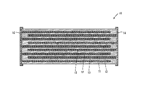
[FIG. 1] Sectional view of a piezoelectric element of an embodiment.
DESCRIPTION OF EMBODIMENTS
[0011]
[Summary of embodiment]
(1) The piezoelectric element disclosed by the present specification has a
piezoelectric body and an electrode in contact with the piezoelectric body,
the piezoelectric
body being formed of a lead-free piezoelectric ceramic composition which
includes a primary
phase formed of an alkali niobate-based perovskite oxide represented by a
compositional
formula (Al aM1b)c(NbaiMnaTid3Zrd4Hfd5)03+e (wherein element Al represents at
least one
species among the alkali metals; element M1 represents at least one species
among Ba, Ca,
CA 03218650 2023- 11- 9
4
and Sr; the following conditions: 0<a<1, 0<b<1, a+b=1, 0.80<c<1.10, 0<dl<1,
0<d2<1,
0<d3<1,014<1, 1:1d5<1, and dl+d2+d3+d4+d5=1, are satisfied; and e represents a
value
showing the degree of deficiency or excess of oxygen) and which satisfies the
condition:
b/(d3+d4+d51, and the electrode containing a base metal as a main component.
[0012]
The piezoelectric element production method disclosed by the present
specification
includes a calcination step of mixing raw materials of a lead-free
piezoelectric ceramic
composition which includes a primary phase formed of an alkali niobate-based
perovskite oxide
represented by a compositional formula (Al aMlb)c(NbchMnaTid3Zrdallfd5)03+e
(wherein
element Al represents at least one species among the alkali metals; element M1
represents at
least one species among Ba, Ca, and Sr; the following conditions: 0<a<1,
0<b<1, a+b=1,
0.80<c<1.10, 0<dl<1, 0<d2<1, 0<d3<1, 0izI4.<1, 0izi5<1, and dl+d2+d3+d4+d5=1,
are
satisfied; and e represents a value showing the degree of deficiency or excess
of oxygen) and
which satisfies the condition: b/(d3+d4+d51, and firing the raw materials, to
thereby yield a
calcined powder; a shaping step of forming a compact containing the calcined
powder; an
electrode formation step of forming, on the compact, an electrode layer
containing a base metal
as a main component; and a co-firing step of firing the compact together with
the electrode layer
in a reducing atmosphere.
[0013]
According to the aforementioned technical features, suitable amounts of Ti,
Zr, and
Hf are incorporated into B sites (niobium sites) of the alkali niobate-based
perovskite oxide,
whereby sinterability to form the piezoelectric body is improved. As a result,
dielectric loss is
lowered, and insulation performance is improved.
[0014]
Conceivably, when Mn serving as an acceptor forms a solid solution in B sites,
loss
of electric charges attributable to oxygen vacancy provided during firing in a
reducing
atmosphere can be compensated. In this case, dielectric loss is lowered, and
insulation
performance is improved. However, difficulty is encountered in formation of a
solid solution of
Mn with an alkali niobate-based perovskite oxide, and Mn tends to segregate to
form a foreign
phase in the lead-free piezoelectric ceramic composition. When Ba, Ca, and Sr
are incorporated
into A sites (alkali sites) to form a solid solution, piezoelectric
performance is enhanced.
However, since Ba, Ca, and Sr serve as donors, the piezoelectric body may
assume a
semiconducting feature, possibly resulting in a disadvantageous drop in
insulation performance.
CA 03218650 2023- 11- 9
5
[0015]
Also conceivably, by adjusting compositional proportions of Ti, Zr, and Hf to
Ba,
Ca, and Sr to satisfy the condition: b/(d3+d4+d 5)1, a semiconducting
phenomenon attributed
to incorporation of Ba, Ca, and Sr into A sites to form a solid solution is
suppressed, while
suitable amounts of Ti, Zr, Hf, and Mn are incorporated to form a solid
solution. In this case,
dielectric loss is lowered, and insulation performance is improved.
[0016]
2) In the piezoelectric element of 1) above, the ratio by mole of Mn atoms
contained
in the primary phase to Nb atoms contained in the primary phase (Mn/Nb) may be
0.003 or
more.
[0017]
In the piezoelectric element production method of 1) above, in the calcination
step,
the ratio by mole of Mn atoms contained in the mixture of the raw materials to
Nb atoms
contained in the mixture of the raw materials (Mn/Nb) may be 0.005 or more.
[0018]
By adjusting the ratio by mole of Mn atoms to Nb atoms in the above manner,
the
dielectric loss of the piezoelectric body can be reliably reduced, to thereby
improve insulation
performance.
[0019]
3) In the piezoelectric element of 1) above, crystal grains of the alkali
niobate-based
perovskite oxide contained in the primary phase may have a mean grain size
less than 6 pm.
[0020]
When the mean grain size of the crystal grains is less than 6 lam, grain
boundary
resistance increases. Thus, an undesired drop in piezoelectric property can be
prevented.
[0021]
4) In the piezoelectric element of 1) above, the lead-free piezoelectric
ceramic
composition may further include a secondary phase formed of one member of a
compound
represented by compositional formula A2i_xTii_xNbi+x05 (wherein element A2 is
at least one
species among the alkali metals, and the condition: 1:1)(0 .15 is satisfied)
and a compound
represented by compositional formula A3Ti3Nb09 (wherein element A3 is at least
one species
among the alkali metals).
[0022]
According to the above technical feature, the piezoelectric performance can be
CA 03218650 2023- 11- 9
6
further enhanced, as compared with the case in which the lead-free
piezoelectric ceramic
composition includes no secondary phase.
[0023]
5) The piezoelectric element of 1) above may have a structure in which the
piezoelectric body and the electrode are alternately stacked.
[0024]
[Details of embodiment]
Specific examples of the techniques disclosed in the present specification
will now
be described with reference to the drawings. Notably, the examples should not
be construed as
limiting the invention thereto, and the scope of the present invention is
defined by the claims.
It is also intended that the present invention encompasses all modifications
within the
meanings and scopes equivalent to those of the claims.
[0025]
<Embodiment>
[Piezoelectric element 10]
A piezoelectric element 10 of the present embodiment includes piezoelectric
layers 11
(an example of the piezoelectric body); a plurality of internal electrodes 12,
13 (examples of the
electrodes) which are in contact with the piezoelectric layers 11; and two
external electrodes 14,
15 which are connected to the internal electrodes 13, 12. The piezoelectric
layers 11 are formed
from a lead-free piezoelectric ceramic composition including a primary phase
formed of an
alkali niobate-based perovskite oxide. The internal electrodes 12, 13 are
formed mainly from a
base metal, such as Ni (nickel). The piezoelectric layers 11 and the internal
electrodes 12, 13
are alternately stacked. More specifically, the piezoelectric layers 11 and
the internal electrodes
12, 13 are stacked in the stacking order of the piezoelectric layer 11, the
internal electrode 12,
the piezoelectric layer 11, the internal electrode 13, the piezoelectric layer
11, and so forth. One
piezoelectric layer 11 is sandwiched by two internal electrodes 12, 13. The
two external
electrode 14, 15 are disposed on the outer surface of the stacked body
including the
piezoelectric layers 11 and the internal electrodes 12, 13. Of two internal
electrodes 12, 13
which are in contact with one piezoelectric layer 11, one internal electrode
12 is connected, at
its one end, to one external electrode 14, and the other internal electrode 13
is connected, at its
one end, to the other external electrode 15. Through application of a voltage
between the
external electrodes 14, 15, the piezoelectric layers 11 expand and contract,
whereby the entirety
of the piezoelectric element 10 expands and contracts.
CA 03218650 2023- 11- 9
7
[0026]
[Technical feature of lead-free piezoelectric ceramic composition]
The lead-free piezoelectric ceramic composition forming the piezoelectric
layers 11
includes a primary phase formed of an alkali niobate-based perovskite oxide
which exhibits a
piezoelectric property. The alkali niobate-based perovskite oxide of the
present embodiment is
represented by the following compositional formula (1).
[0027]
(AlaMlb)c(Nbd1M1d2Tid3Zrd4llfd5)03+e =.= (1)
[0028]
In formula (1), element Al is at least one species among alkali metals, and
element
M1 is at least one species among alkaline earth metals of Ca (calcium), Sr
(strontium), and Ba
(barium).
[0029]
In the above compositional formula (1), element Al and element M1 are located
in
A sites (alkali sites) of the perovskite structure, and Nb (niobium), Mn
(manganese), Ti
(titanium), Zr (zirconium), and Hf (hafnium) are located in B sites.
[0030]
In the compositional formula (1), coefficients a to e are selected from the
values
which are preferred from the viewpoints of electrical characteristics and
piezoelectric
characteristics (in particular, piezoelectric constant d33) of the lead-free
piezoelectric ceramic
composition, so long as the coefficients a to e ensure establishment of the
perovskite structure.
[0031]
Specifically, coefficients a and b satisfy the conditions: 0<a<1, 0<b<1, and
a+b=1.
However, the cases of a=0 (i.e., the composition containing no alkali metal)
and b=0 (i.e., the
composition containing none of Ca, Sr, and Ba) are excluded.
[0032]
Coefficient c with respect to the entire A sites satisfies 0.80<c<1.10, and is
preferably 0. 8,4c1.08, more preferably 0.88c1.07.
[0033]
Coefficients dl, d2, d3, d4, and d5 satisfy the conditions: 0<dl<1, 0<d2<1,
0<d3<1,014<1,015<1, and dl+d2+d3+d4+d5=1. However, the cases of d1=0 (i.e.,
the
composition containing no Nb, d2=0 (i.e., the composition containing no Mn),
and d3=0 (i.e.,
the composition containing no Ti) are excluded. Coefficient d4 with respect to
Zr and
CA 03218650 2023- 11- 9
8
coefficient d5 with respect to Hf may be 0 (i.e., the composition not
containing Zr and/or Hf).
[0034]
In coefficient (3+e) with respect to oxygen, the value of e is a positive or
negative
value showing deviation (deficiency or excess) from the intrinsic value of 3
with respect to
oxygen. Coefficient (3+e) with respect to oxygen may be a value which allows
the primary
phase to have a perovskite oxide structure. Typically, coefficient e is 0, and
preferably satisfies
1:1eD:1.1. Notably, coefficient e may also be calculated from the composition
of the primary
phase to meet the electrically neutral condition. However, needless to say, a
composition of the
primary phase which is slightly deviated from the electrically neutral
condition is also
allowable.
[0035]
Coefficients b, d3, d4, and d5 satisfy the condition: b/(d3+d4+d5)1. When
coefficients b, d3, d4, and d5 satisfy the condition, a lead-free
piezoelectric ceramic
composition which exhibits low dielectric loss and high insulation performance
can be yielded.
A conceivable reason for this is as follows.
[0036]
Since suitable amounts of Ti, Zr, and Hf are incorporated into B sites
(niobium sites)
of the alkali niobate-based perovskite oxide, sinterability to form the
piezoelectric body is
improved. As a result, dielectric loss is lowered, and insulation performance
is improved.
[0037]
Also conceivably, when Mn serving as an acceptor forms a solid solution in B
sites,
loss of electric charges attributable to oxygen vacancy provided during firing
in a reducing
atmosphere can be compensated. In this case, dielectric loss is lowered, and
insulation
performance is improved. However, difficulty is encountered in formation of a
solid solution of
Mn with an alkali niobate-based perovskite oxide, and Mn tends to segregate to
form a foreign
phase in the lead-free piezoelectric ceramic composition. When Ba, Ca, and Sr
are incorporated
into A sites (alkali sites) to form a solid solution, piezoelectric
performance is enhanced.
However, since Ba, Ca, and Sr serve as donors, the piezoelectric body may
assume a
semiconducting feature, possibly resulting in a disadvantageous drop in
insulation performance.
[0038]
Also conceivably, by adjusting compositional proportions of Ti, Zr, and Hf to
Ba,
Ca, and Sr to satisfy b/(d3+d4+d 5)1, a semiconducting phenomenon attributed
to
incorporation of Ba, Ca, and Sr into A sites to form a solid solution is
suppressed, while suitable
CA 03218650 2023- 11- 9
9
amounts of Ti, Zr, Hf, and Mn are incorporated to form a solid solution. In
this case, dielectric
loss is lowered, and insulation performance is improved.
[0039]
The alkali niobate-based perovskite oxide represented by the aforementioned
compositional formula (1) preferably contains, as element Al, at least one
species among K
(potassium), Na (sodium), and Li (lithium). When the above oxide contains at
least one species
of K, Na, and Li as element Al and at least one species of Ca, Sr, and Ba as
element Ml,
compositional formula (1) can be transformed into the following compositional
formula (1a).
[0040]
(Ka1Naa2Lia3Cab1Srb2Bab3)c(Nbd1Mn12Tid3Zrd4ilf15)03+e = = = (1a)
[0041]
The aforementioned compositional formula (1) is equivalent to the above
formula
(la), and the conditions: al +a2+a3=a and bl+b2+b3=b, are satisfied.
Typically, coefficients al
and a2 with respect to K and Na satisfy the conditions: 0<alD16 and 0<a2D16,
respectively.
Coefficient a3 with respect to Li may be 0 and is preferably 0<a3D12, more
preferably
0<a3D11.
[0042]
Among the alkali niobate-based perovskite oxides represented by compositional
formula (la), those containing K, Na, and Nb as main metallic components are
called "KNN"
or "KNN material." A lead-free piezoelectric ceramic composition, which is
produced by use of
such an oxide, can exert excellent piezoelectric characteristics, electric
characteristics,
insulation performance, and durability at high temperatures and does not
exhibit steep
variation in these characteristics within a temperature range of -50 C to +150
C. A typical
composition of the primary phase is (K, Na, Li, Ca, Ba)c(Nb, Mn, Ti, Zr,
H003+e.
[0043]
The lead-free piezoelectric ceramic composition of this embodiment may further
include a secondary phase formed of one member of an oxide represented by the
following
compositional formula (2) and an oxide represented by the following
compositional formula
(3).
[0044]
A21Tii_xNbi+x05 === (2)
A3Ti3Nb09 === (3)
[0045]
CA 03218650 2023- 11- 9
10
In compositional formula (2), element A2 is at least one species among alkali
metals, preferably at least one species among K, Rb (rubidium), and Cs
(cesium). Coefficient x
satisfies the condition: 1:1)(0 .15. When coefficient x satisfies this
condition, the secondary
phase has a stable structure, thereby yielding a uniform crystalline phase.
From the viewpoint of
structural stability of the secondary phase, coefficient x preferably
satisfies the condition:
1:1)(0.15 in the case in which element A2 is K or Rb, and the condition: 00.10
in the case in
which element A2 is Cs.
[0046]
In compositional formula (3), element A3 is at least one species among alkali
metals, preferably at least one species among K, Rb, and Cs.
[0047]
The secondary phase itself has no piezoelectric property. However, when the
secondary phase is co-present with the primary phase, sinterability and
insulation
performance can be enhanced. Also, the secondary phase may prevent phase
transition within
a range of -50 C to +150 C. The secondary phase assumes a compound having a
layer
structure (i.e., a layer compound). Conceivably, the layer structure of the
compound may be a
factor for enhancing insulation performance of the piezoelectric ceramic
composition and
preventing phase transition.
[0048]
The secondary phase content may be more than 0 mol% and less than 20 mol%, and
is preferably 2 mol% or more and 15 mol% or less, more preferably 2 mol% or
more and 10
mol% or less.
[0049]
Among the oxides represented by compositional formula (2) or (3), those
containing
Nb, Ti, and K as main metallic components are called "NTK material." By use of
such an
oxide, a lead-free piezoelectric ceramic composition which is inexpensive and
exhibits
excellent piezoelectric characteristics can be provided.
[0050]
The ratio by mole of Mn atoms contained in the primary phase to Nb atoms
contained in the primary phase (Mn/Nb) is preferably 0.003 or more. By
adjusting the mole
ratio in the above manner, dielectric loss of the piezoelectric layers 11 can
be reliably reduced,
thereby improving insulation performance.
[0051]
CA 03218650 2023- 11- 9
11
The crystal grains of the alkali niobate-based perovskite oxide contained in
the
primary phase preferably have a mean grain size less than 6 gm. When the mean
grain size of
the crystal grains is less than 6 gm, grain boundary resistance increases.
Thus, an undesired
drop in piezoelectric property can be prevented.
[0052]
[Method of producing piezoelectric element 101
An example of the method of producing the aforementioned piezoelectric element
10
will next be described.
[0053]
1. Calcination step
First, essential ingredients for producing a primary phase are chosen from
powder-
form raw materials, and weighed so as to attain a target composition. The
powder-form raw
materials may be an oxide, a carbonate salt, or a hydroxide of an element
forming the primary
phase. In this procedure, the ratio by mole of Mn atoms contained in the
powder-form raw
materials of the primary phase to Nb atoms contained in the powder-form raw
materials of the
primary phase (Mn/Nb) is adjusted to be 0.005 or more. To these powder-form
raw materials,
ethanol is added, and the mixture is agitated under wet conditions by means of
a ball mill for
preferably 15 hours or longer, to thereby prepare a slurry. In one mode, the
thus-prepared slurry
is dried, and the dry powder mixture is calcined at 600 to 1,000 C in air for
1 to 10 hours, to
thereby yield a calcined product of the primary phase (calcination step).
[0054]
No particular limitation is imposed on the upper limit of the ratio by mole of
Mn
atoms contained in the powder-form raw materials of the primary phase to Nb
atoms
contained in the powder-form raw materials of the primary phase (Mn/Nb), but
the ratio by
mole (Mn/Nb) is preferably 0.1 or less. When the ratio by mole (Mn/Nb) is in
excess of 0.1,
sintering may be impeded.
[0055]
Separately, essential ingredients for producing a secondary phase are chosen
from
powder-form raw materials, and weighed so as to attain a target composition.
The powder-form
raw materials may be an oxide, a carbonate salt, or a hydroxide of an element
forming the
secondary phase. To these powder-form raw materials, ethanol is added, and the
mixture is
agitated under wet conditions by means of a ball mill for preferably 15 hours
or longer, to
thereby prepare a slurry. In one mode, the thus-prepared slurry is dried, and
the dry powder
CA 03218650 2023- 11- 9
12
mixture is calcined at 600 to 1,000 C in air for 1 to 10 hours, to thereby
yield a calcined product
of the secondary phase.
[0056]
Subsequently, a calcined product of the primary phase and that of the
secondary
phase are weighed, and a dispersant, a binder, and an organic solvent (e.g.,
toluene) are added
to the weighed mixture. The resultant mixture is pulverized and agitated, to
thereby form a
slurry. Then, the slurry is formed into a sheet through a doctor blade
technique or the like, to
thereby form a ceramic green sheet (an example of the compact) (shaping step).
[0057]
Next, a conductive paste for forming an internal electrode is applied to a
surface of
the ceramic green sheet through a technique, such as screen printing, to
thereby form an
electrode layer serving as an internal electrode (electrode formation step).
The electrode layer
is mainly formed of a base metal (e.g., Ni).
[0058]
A plurality of units of the ceramic green sheet on which the electrode layer
has been
formed are stacked together, and another ceramic green sheet having no
electrode layer is
placed on each of the surface of the stacked body. The product is pressed, to
thereby yield a
stacked body in which ceramic green sheets and electrode layers have been
alternately stacked.
The stacked body is cut into a shape of interest and subjected to a
debindering treatment (e.g.,
maintaining the stacked body at 200 to 400 C for 2 to 10 hours).
[0059]
After debindering, the stacked body is fired under specific conditions (e.g.,
maintaining at 900 to 1,200 C in a reducing atmosphere for 2 to 5 hours). The
oxygen partial
pressure of the firing atmosphere is adjusted so that the electrode layers are
not oxidized (co-
firing step).
[0060]
After firing, Au external electrodes are formed on the outer surface of the
stacked
body through a technique, such as sputtering, and the product is subjected to
a polarization
treatment, to thereby fabricate a piezoelectric element.
[0061]
Notably, the production method as described above is a merely an exemplary
method, and various other steps and treatment conditions for producing a
piezoelectric
element may be employed. In the above production procedure, a calcined product
of the
CA 03218650 2023- 11- 9
13
primary phase and that of the secondary phase are separately formed, and the
two products are
mixed, followed by firing. However, in an alternative method, raw materials of
the primary
phase and those of the secondary phase are mixed at such a ratio that the
target compositional
proportions of the finally obtained lead-free piezoelectric ceramic
composition are attained,
and the thus-prepared mixture is fired. Through the former method, rigorous
control of the
composition of the primary phase and that of the secondary phase can be easily
achieved,
whereby the yield of the lead-free piezoelectric ceramic composition can be
enhanced.
[0062]
The lead-free piezoelectric ceramic composition and the piezoelectric element
according to the present embodiment find various uses including vibration
sensing, pressure
sensing, oscillation, and piezoelectric devices. Specific examples include
sensors for detecting
various vibrations (e.g., a knocking sensor and a combustion pressure sensor);
piezoelectric
devices such as an oscillator, an actuator, and a filter; high-voltage
generators; micro power
supplies; driving units; position control systems; vibration dampers; and
fluid discharge
systems (e.g., a paint ejector and a fuel ejector). In addition, the lead-free
piezoelectric ceramic
composition and the piezoelectric element according to the present embodiment
are particularly
suitable for uses requiring extremely high heat resistance (e.g., a knocking
sensor and a
combustion pressure sensor).
[0063]
In the present embodiment, the piezoelectric element 10 has a configuration in
which piezoelectric layers 11 and internal electrodes 12, 13 are alternately
stacked.
Alternatively, the piezoelectric element may have a single-layer structure
including one layer of
a piezoelectric body, and electrodes provided on the piezoelectric body.
[0064]
<Test Examples>
1. Test Example 1
(1) Sample preparation
Powders of K2CO3, Na2CO3, and Nb2O5 were weighed so that coefficients f and g
of
the following compositional formula (2) were adjusted to specific values shown
in Table 1. The
weighed powders were mixed together.
[0065]
(KfNag)Nb03 ¨ (2)
[0066]
CA 03218650 2023- 11- 9
14
Separately, BaCO3 powder, CaCO3 powder, and SrCO3 powder were weighed so
that the total mol% of Ba atoms, Ca atoms, and Sr atoms with respect to Nb
atoms present in
the Nb2O5 powder was adjusted to a specific value shown in Table 1. An
essential ingredient or
ingredients was/were added to the mixture of K2CO3, Na2CO3, and Nb2O5. Also,
Mn02
powder, TiO2 powder, ZrO2 powder, and Hf02 powder were weighed so that the
mol% of
atom of each additional metal with respect to Nb atoms present in the Nb2O5
powder was
adjusted to a specific value shown in Table 1, and the ingredients were added
to the mixture of
K2CO3, Na2CO3, and Nb2O5.
[0067]
In each case, ethanol was added to the thus-prepared powder-form raw material,
and
the resultant mixture was agitated under wet conditions by means of a ball
mill for 15 hours or
longer, to thereby prepare a slurry. The slurry was dried, and the dry powder
mixture was
calcined at 600 to 1,000 C in air for 1 to 10 hours, to thereby yield a
calcined product powder.
[0068]
To the thus-obtained calcined product powder, a dispersant, a binder, and an
organic
solvent (e.g., toluene) were added, and the resultant mixture was pulverized
and agitated, to
thereby form a slurry. Thereafter, the slurry was formed into a sheet through
a doctor blade
technique, to thereby form ceramic green sheets. A plurality of the ceramic
green sheets were
stacked under application of pressure, and the pressed body was cut into a
disk-form compact.
[0069]
Onto each surface of the compact, a conductive paste for forming an electrode
was
applied through screen printing, to thereby from an electrode layer (electrode
formation step).
As shown in Table 2, the electrode component content of the conductive pastes
used for forming
an electrode was adjusted to 100% (Ni) in the case of samples No. 1 to 24, and
90 mass% (Cu)
and 10 mass% (Ni) in the case of sample No. 25.
[0070]
Each of the compacts provided with electrode layers was maintained at 200 to
400 C for 2 to10 hours for debindering. Then, co-firing was performed at 900
to 1,200 C for 2
to 5 hours in a reducing atmosphere in which the oxygen partial pressure was
controlled to
inhibit oxidation of the electrode layers. The thus-obtained fired product was
subjected to a
polarization treatment in silicone oil at 50 C under application of an
electric field of 5 kv/mm,
to thereby provide a sample. The obtained sample was a piezoelectric element
having a
piezoelectric body and an electrode layer formed on each surface of the
piezoelectric body, in
CA 03218650 2023- 11- 9
15
which the piezoelectric body was formed from a lead-free piezoelectric ceramic
composition
containing an alkali niobate-based perovskite oxide represented by
compositional formula (1a).
[0071]
[Table 1]
Ml ELEMENT
Ti Zr Hf
Mn
SAMPLE Ba Ca Sr
f g
No. AMOUNT AMOUNT AMOUNT AMOUNT AMOUNT AMOUNT
AMOUNT
monto moN6 moN6 monto monto moN6 monto
1 0.48 0.52 6 2 2 0
5
2 0.48 0.52 3 3 2 2 0
5
3 0.48 0.52 2 2 2 0
0
4 0.48 0.52 2 - 0 5 0
5
0.48 0.52 4 - - 2 2 0 5
6 0.48 0.52 2 2 2 0
5
7 0.48 0.52 2 - - 4 2 0
5
8 0.48 0.52 1 - - 5 1 0
5
9 0.48 0.52 2 1 2 0
5
0.48 0.52 2 - - 2 2 0 0.1
11 0.48 0.52 2 2 2 0
0.5
12 0.48 0.52 2 2 2 0
1
13 0.48 0.52 2 2 2 0
7
14 0.48 0.52 2 - - 4 0 0
5
0.48 0.52 2 1 3 0 5
16 0.48 0.52 2 2 2 0
1
17 048 052 - - 2 2 2 0
1
18 0.48 0.52 1 1 2 2 0
1
19 0.48 0.52 7 5 2 0
5
0.10 0.90 2 - - 2 2 0 5
21 0.70 0.30 2 2 2 0
5
22 0.48 0.52 5 5 7 0
5
23 0.48 0.52 4 2 0 2
5
24 0.48 0.52 4 2 1 1
5
0.48 0.52 4 2 2 0 5
5
[0072]
(2) Test method
Each of the produced samples was analyzed by means of an impedance analyzer
(E4990A, product of Keysight Technologies). By use of an electrostatic
capacity at room
CA 03218650 2023- 11- 9
16
temperature and 1 kHz, dielectric loss tano was calculated. In addition,
electromechanical
coupling coefficient kp was determined through a resonance-antiresonance
system. When a
sample exhibited a dielectric loss fano of 3.0% or less and an
electromechanical coupling
coefficient kp of 20% or higher, the sample was evaluated as a good (i.e.,
nondefective) product.
[0073]
Also, each of the produced samples was subjected to a dielectric breakdown
test. In
a specific test procedure, an electric field of 5 kv/mm was applied for 30
minutes or longer to
the sample placed in silicon oil at 50 C, and occurrence of dielectric
breakdown was checked.
The case of occurrence of dielectric breakdown was assessed as rating "X" and
the case of no
occurrence of dielectric breakdown was assessed as rating "0."
[0074]
(3) Results
Pmi/(PTi+Pzr+PHf) of each sample was calculated, wherein Pmi is a total mol%
of Ba
atoms, Ca atoms, and Sr atoms with respect to Nb atoms present in the raw
material powder
mixture weighed in 1.(1) above, and PT, Pzr, and Pllf are a mol% of Ti atoms,
a mol% of Zr
atoms, and a mol% of Hf atoms, with respect to Nb atoms, respectively.
Further, each sample
was subjected to elemental analysis by means of an electron probe
microanalyzer (EPMA).
The analysis was performed at three points (grains) of the primary phase with
a beam size of
(I) 1 lam, whereby the ratio by mole of Mn atoms contained in the main phase
to Nb atoms
contained in the main phase was determined. The ratio by mole of Mn atoms to
Nb atoms
(Mn/Nb) was an averaged values determined at the three points. Table 2 shows
these values,
along with values of dielectric loss fano, electromechanical coupling
coefficient kp, and
results of the dielectric breakdown test.
[0075]
CA 03218650 2023- 11- 9
17
[Table 2]
ELECTROMECH.
DIELECTRIC
SAMPLE
INSU-
ELECTRME Pmii(P-ri+Pzr+PHO Mn/Nb COUPLING COEFF.
LOSS
No. kp
LATION tan 6
Ey,
Ey,
1 Ni 1.5 0.031 - x
5.3
2 Ni 1.5 0.031 - x
6.1
3 Ni 0.5 0.000 x
7.3
4 Ni 0.4 0.032 - x
10.3
Ni 1.0 0.031 30 0 2.4
6 Ni 0.5 0.031 31 0
2.3
7 Ni 0.3 0.032 33 0
1.9
8 Ni 0.2 0.032 31 0
2.2
9 Ni 0.7 0.031 28 0
2.3
Ni 0.5 0.001 - x 5.8
11 Ni 0.5 0.003 26 0
2.8
12 Ni 0.5 0.006 28 0
2.6
13 Ni 0.5 0.044 27 0
2.8
14 Ni 0.5 0.031 30 0
2.8
Ni 0.5 0.031 25 0 2.4
16 Ni 0.5 0.006 27 0
2.7
17 Ni 0.5 0.006 26 0
2.8
18 Ni 0.5 0.006 26 0
2.7
19 Ni 1.0 0.032 25 0
2.8
Ni 0.5 0.031 24 0 2.9
21 Ni 0.5 0.031 24 0
2.5
22 Ni 0.4 0.034 33 0
2.0
23 Ni 1.0 0.031 30 0
2.2
24 Ni 1.0 0.031 29 0
2.3
Cu:Ni=9:1 1.0 0.031 28 0
2.6
[0076]
Theoretically, Ca atoms, Sr atoms, and Ba atoms which are present in raw
material
5 powders completely enter the A sites of the alkali niobate-based
perovskite oxide, and Ti
atoms, Zr atoms, and Hf atoms completely enter the B sites of the alkali
niobate-based
perovskite oxide. Therefore, the total mol% of Ba atoms, Ca atoms, Sr atoms
(Pmi) may
correspond to the sum of coefficients bl, b2, and b3 to Ba, Ca, and Sr of
compositional formula
(la) (i.e., coefficient b of compositional formula (1)), and the mol% of Ti
atoms, Zr atoms, and
10 Hf atoms may correspond to coefficient d3, d4, and d5 to Ti, Zr, and Hf
in compositional
formula (1), respectively. Thus, the equation in terms of mol%: P /(13 +P +P 1
may be
_ mi. ,_ Ti - Zr - Hf,,
equivalent to the equation: b/(d3+d4+d5), regarding coefficients b, d2, and d3
of
compositional formula (1).
CA 03218650 2023- 11- 9
18
[0077]
Samples Nos. 1 and 2, having a P /(P +P +P 1
- mi. Ti Zr Hfi value (i.e., b/(d3+d4+d5) value)
of 1 or more, exhibited a dielectric loss of 3.0% or more and underwent
dielectric breakdown in
the dielectric breakdown test. Also, sample No. 3, containing no Mn, exhibited
a dielectric loss
of 3.0% or more and underwent dielectric breakdown in the dielectric breakdown
test.
Similarly, sample No. 4, containing no Ti, exhibited a dielectric loss of 3.0%
or more and
underwent dielectric breakdown in the dielectric breakdown test. Furthermore,
sample No. 10,
having a mol% of Mn atoms contained in the raw material mixture to Nb atoms
contained in the
raw material powder of 0.1% (i.e., having a mol ratio of Mn atoms contained in
the raw material
mixture to Nb atoms contained in the raw material mixture (Mn/Nb) of 0.001),
exhibited a
dielectric loss of 3.0% or more and underwent dielectric breakdown in the
dielectric breakdown
test.
[0078]
Each of samples Nos. 5 to 9 and Nos. 11 to 25 essentially contained element Al
(at
least one of alkali metals), element M1 (at least one of Ba, Ca, and Sr), and
Mn and Ti. These
samples had a P in) +P +P 1
- mi. Ti Zr Hfi value (i.e., b/(d3+d4+d5) value) less than 1; a mol% of Mn
atoms contained in the raw material mixture to Nb atoms contained in the raw
material mixture
of 0.5% or more (i.e., having a mol ratio of Mn atoms contained in the raw
material mixture to
Nb atoms contained in the raw material mixture (Mn/Nb) of 0.005 or more); and
a ratio by
mole of Mn atoms to Nb atoms contained in the primary phase (Mn/Nb) of 0.003
or more.
These samples were found to exhibit a dielectric loss of 3.0% or less and an
electromechanical
coupling coefficient of 20% or higher, and to undergo no dielectric breakdown
in the dielectric
breakdown test, indicating excellent piezoelectric characteristics.
[0079]
2. Test Example 2
(1) Preparation of samples and test method
In a manner similar to that of Test Example 1, samples Nos. 26 to 29, having
the
same composition as that of sample No. 5, were produced (see Table 3). These
samples were
prepared through a firing step employing various firing temperatures. As a
result, the grain
size of crystal grains forming the alkali niobate-based perovskite oxide was
modified.
[0080]
CA 03218650 2023- 11- 9
19
[Table 3]
MI.
ELEMENT Ti Zr Mn
SAMPLE Ba
f g P pn /(P
Ti+P Zr+P HO
No. AMOUNT AMOUNT AMOUNT AMOUNT
nnol% nnol% nnol% nnol%
0.48 0.52 2 2 2 5 0.5
26 0.48 0_52 2 2 2 5 0_5
27 0.48 0.52 2 2 2 5 0.5
28 0.48 0.52 2 2 2 5 0.5
29 0.48 0.52 2 2 2 5 0.5
[0081]
The thus-prepared samples were subjected to image analysis (x5,000) by means
of
5 an SEM (TM4000 Plus, product of Hitachi High-Tech Corporation). In each
image, the
average value of grain size of crystal grains observed in the image was
employed as a mean
grain size. The prepared samples were subjected to the same test as Test
Example 1, whereby
dielectric loss tano and electromechanical coupling coefficient kp were
determined. The same
dielectric breakdown test was also performed.
[0082]
(2) Results
Table 4 shows dielectric loss tano, electromechanical coupling coefficient kp,
and
the results of dielectric breakdown test of the samples, along with mean
particle size.
[0083]
[Table 4]
SAMPLE MEAN GRAIN ELECTROMECH.
COUPLING DIELECTRIC LOSS
SIZE COEFF. kp INSULATION tan 6
No. um cyo cyo
5 2.3 31 0 2.3
26 4.5 28 0 2.6
27 1.5 26 0 2.1
28 5.3 25 0 2.8
29 6.0 18 x 3.8
[0084]
Sample No. 29, having a mean grain size of crystal grains of 6 gm, exhibited a
dielectric loss of 3.0% or more and underwent dielectric breakdown in the
dielectric breakdown
CA 03218650 2023- 11- 9
20
test. In contrast, Samples No. 5 and Nos. 26 to 28, having a mean grain size
of crystal grains
less than 6 gm, exhibited a dielectric loss of 3.0% or less and an
electromechanical coupling
coefficient of 20% or higher, and underwent no dielectric breakdown in the
dielectric
breakdown test, indicating excellent piezoelectric characteristics.
REFERENCE SIGNS LIST
[0085]
10: piezoelectric element
11: piezoelectric layer (piezoelectric body)
12, 13: internal electrode (electrode)
CA 03218650 2023- 11- 9