Note : Les descriptions sont présentées dans la langue officielle dans laquelle elles ont été soumises.
WO 2023/278669
PCT/US2022/035681
1
SOLID-STATE DIRECT CAVITY COMBINER (DCC) TRANSMITTER SYSTEM
FOR PROVIDING MEGAWATTS OF POWER
RELATED APPLICATIONS
This application claims benefit of and priority to U.S. Provisional
Application
Serial No. 63/216,583 filed June 30, 2021, under 35 U.S.C. 119, 120, 363,
365, and 37
C.F.R. 1.55 and 1.78, which is incorporated herein by this reference.
FIELD OF THE INVENTION
This subject invention relates to a solid-state direct cavity combiner (DCC)
transmitter system.
BACKGROUND OF THE INVENTION
A solid-state Direct Cavity Combiner (DCC) transmitter combines the RF output
of many RF transistors in a large resonant cavity operating in a range of
predetermined
frequencies. To date, no one has successfully created a compact, reliable,
solid-state DCC
transmitter capable of delivering megawatts of heating power at RF frequencies
into
either present experimental or future commercial nuclear fusion power plants.
Conventional RF power technology to provide such high-power at RF frequencies
for nuclear fusion includes vacuum tubes and modular solid-state amplifiers.
Both of
these technologies may fail to deliver the needed power at RF frequencies for
different
reasons.
One conventional approach to delivering RF power needed for plasma heating
CA 03224407 2023- 12-28
WO 2023/278669
PCT/US2022/035681
2
relies on high-power vacuum tubes (tetrodes). Vacuum electronic devices may
fail
because of inherent tube characteristics and vanishing marketplace issues,
such as tuning,
stability, lifetime, unreliable supply chain and the like. The large tetrodes
or vacuum
tubes are in serious risk of being abandoned by industry as the techniques
required to
build them are lost through retirement of the key engineers and technicians.
Another conventional approach to delivering RF power needed for plasma heating
is modular solid-state amplifiers which use multi-stage power combination
(which may
or may not include binary combining) to combine the output of many individual
transistor amplifiers. Modular solid-state amplifiers may fail due to
electrical and RF
control difficulties (generation and combination of a distributed system),
mechanical
complexity, and a very large footprint. While conventional solid-state
transmitters have
been demonstrated at hundreds of kilowatts, state-of-the-art conventional high-
power
transmitters remain excessively large and complex. The leading manufacturer of
such
devices has indicated they would not repeat the current approach of combining
many 100
kW units.
SUMMARY OF THE INVENTION
In one aspect, a solid-state direct cavity combiner (DCC) transmitter system
for
providing megawatts of power is featured. The system includes a resonant
cavity
including at least one high-power output transmission line, hundreds of high-
power
transistors each generating an amount of power input directly into the
resonant cavity,
and a plurality of modules each including at least one pair of high-power
transistors
CA 03224407 2023- 12-28
WO 2023/278669
PCT/US2022/035681
3
differentially driving a transmission line and a coupling loop. Each said
transmission line
and coupling loop extends into the resonant cavity to match an impedance of
each said
high-power transistor of each said module to an impedance of said resonant
cavity to
electromagnetically couple power into the resonant cavity to provide the
megawatts of
power to the high-power output transmission line.
In one embodiment, the megawatts of power may be in the range of about 1 MW
to about 3 MW. Each module includes the transmission line, the coupling loop,
and at
least one pair of high-power transistors. The at least one pair of high-power
transistors
may be symmetrically opposed to provide differential inputs to the
transmission line.
Each module may include two pairs of high-power transistors packaged as a quad
module. Each pair of high-power transistors may be symmetrically opposed to
provide
differential inputs to each transmission line. The plurality of modules may be
positioned
on the resonant cavity to maximize packing density of the high-power
transistors. The
plurality of modules may be positioned at different radii on the end-plate on
the resonant
cavity. Three quad modules may be packaged as a tri-quad module. Each quad
module
may be positioned at a different radii on the end-plate. The tri-quad modules
may be
positioned on the resonant cavity to maximize packing density of the high-
power
transistors. Each tri-quad module may include a power converter to efficiently
power the
high-power transistors from a single high voltage input. The resonant cavity
may include
at least one liquid cooled cavity end-plate including a plurality of coolant
channels. The
resonant cavity may include a plurality of concentric rings of slots disposed
through an
end-plate. Each said transmission line and said coupling loop of each said
module may
CA 03224407 2023- 12-28
WO 2023/278669
PCT/US2022/035681
4
extend through one slot of the plurality of concentric rings of slots. A
predetermined
number of the plurality of modules may be positioned proximate one or more
concentric
rings about the cavity end-plate. The plurality of quad modules may be
positioned
proximate one or more concentric rings about the cavity end-plate. The
plurality of tri-
quad modules may be positioned equally spaced along the concentric rings about
the
cavity end-plate. The megawatts of power may be used for plasma heating in a
fusion
reactor. The plurality of modules may include an electrostatic shield mounted
to an
interior of the resonant cavity to shield each magnetic coupling loop from an
axial
electric field. The plurality of modules may include an overvoltage protection
circuit
configured to prevent damage to the high-power transistors in the event of an
overload.
In another aspect, a solid-state direct cavity combiner (DCC) transmitter
system
for providing megawatts of power is featured. The system includes a resonant
cavity
including at least one high-power output transmission line, hundreds of high-
power
transistors each generating an amount of power input directly into the
resonant cavity,
and a plurality of modules each including a plurality of high-power
transistors, a
transmission line and a coupling loop. The plurality of modules is positioned
at multiple
different radii on an end-plate on the resonant cavity to maximize packing
density of the
high-power transistors. Each transmission line and coupling loop extends into
the
resonant cavity to match an impedance of each said high-power transistor of
each said
module to an impedance of said resonant cavity to electromagnetically couple
power into
the resonant cavity to provide the megawatts of power to the high-power output
transmission line.
CA 03224407 2023- 12-28
WO 2023/278669
PCT/US2022/035681
In one embodiment, the megawatts of power may be in the range of about 1 MW
to about 3 MW. Each module may include the transmission line, the coupling
loop, and at
least one pair of transistors. The pair of high-power transistors may be
symmetrically
opposed to provide differential inputs to the transmission line. Each module
may include
two pairs of high-power transistors packaged as a quad module. Each pair of
high-power
transistors may be symmetrically opposed to provide differential inputs to
each
transmission line. The plurality of modules may be positioned on the resonant
cavity to
maximize packing density of the high-power transistors. The plurality of
modules may be
packaged at different radii on the end-plate on the resonant cavity. Three
quad modules
may be packaged as a tri-quad module. Each quad module may be positioned at a
different radii on the end-plate. Each of the tri-quad modules may be
positioned on the
resonant cavity to maximize packing density of the high-power transistors.
Each tri-quad
module may include a power converter to efficiently power the high-power
transistors
from a single high voltage input. The resonant cavity may include at least one
liquid
cooled cavity end-plate including a plurality of coolant channels. The
resonant cavity
may include a plurality of concentric rings of slots disposed through an end-
plate. Each
said transmission line and said coupling loop of each said module may extend
through
one slot of the plurality of concentric rings of slots. A predetermined number
of the
plurality of modules may be positioned proximate one or more concentric rings
about the
cavity end-plate. A plurality of quad modules may be positioned proximate one
or more
concentric rings about the cavity end-plate. A plurality of tri-quad modules
may be
positioned equally spaced along the concentric rings about the cavity end-
plate. The at
CA 03224407 2023- 12-28
WO 2023/278669
PCT/US2022/035681
6
least one fusion device may include a fusion reactor. The each of the
plurality of modules
may include an electrostatic shield mounted to an interior of the resonant
cavity to shield
each magnetic coupling loop from an axial electric field. The plurality of
modules may
include an overvoltage protection circuit configured to prevent damage to the
high-power
transistors in the event of an overload.
In another aspect, a solid-state direct cavity combiner (DCC) transmitter
system
for providing megawatts of power is featured. The system includes a resonant
cavity
including at least one high-power output transmission line, hundreds of high-
power
transistors each generating an amount of power input directly into the
resonant cavity,
and a plurality of modules each including at least one pair of high-power
transistors
differentially driving a transmission line and a coupling loop. The plurality
of modules
positioned at multiple different radii on an end-plate on the resonant cavity
to maximize
packing density of the high-power transistors. Each transmission line and
coupling loop
extend into the resonant cavity to match an impedance of each said high-power
transistor
of each said module to an impedance of said resonant cavity to
electromagnetically
couple power into the resonant cavity to provide the megawatts of power to the
high-
power output transmission line.
In one embodiment, the megawatts of power may be in the range of about 1 MW
to about 3 MW. Each module may include the transmission line, the coupling
loop, and at
least one pair of transistors packaged as a module. The pair of high-power
transistors may
be symmetrically opposed to provide differential inputs to the transmission
line. Each
module may include two pair power transistors packaged as a quad module. Each
pair of
CA 03224407 2023- 12-28
WO 2023/278669
PCT/US2022/035681
7
high-power transistors may be symmetrically opposed to provide differential
inputs to
each transmission line. The plurality of modules may be positioned on the
resonant cavity
to maximize packing density of the high-power transistors. The plurality of
modules may
be packaged at different radii on the end-plate on the resonant cavity. Three
quad
modules may be packaged as a tri-quad module. Each quad module may be
positioned at
a different radii on the end-plate. Each of the tri-quad modules may be
positioned on the
resonant cavity to maximize packing density of the high-power transistors.
Each tri-quad
module may include a power converter to efficiently power the high-power
transistors
from a single high voltage input. The resonant cavity may include at least one
liquid
cooled cavity end-plate including a plurality of coolant channels. The
resonant cavity
may include a plurality of concentric rings of slots disposed through an end-
plate. Each
said transmission line and said coupling loop of each said module may extend
through
one slot of the plurality of concentric rings of slots. A predetermined number
of the
plurality of modules may be positioned proximate one or more concentric rings
about the
cavity end-plate. The plurality of quad modules may be positioned proximate
one or more
concentric rings about the cavity end-plate. The plurality of tri-quad modules
may be
positioned equally spaced along the concentric rings about the cavity end-
plate. The at
least one fusion device may include a fusion reactor. The plurality of modules
may
include an electrostatic shield mounted to an interior of the resonant cavity
to shield each
magnetic coupling loop from an axial electric field. The plurality of modules
may include
an overvoltage protection circuit configured to prevent damage to the high-
power
transistors in the event of an overload.
CA 03224407 2023- 12-28
WO 2023/278669
PCT/US2022/035681
8
In another aspect, a method for providing megawatts of power with a solid-
state
direct cavity combiner (DCC) transmitter is featured. The method includes
providing a
resonant cavity including at least one high-power output transmission line,
providing
hundreds of high-power transistors each generating an amount of power input
directly
into the resonant cavity, and providing a plurality of modules each including
at least one
pair of high-power transistors differentially driving a transmission line and
a coupling
loop. The method also includes extending each said transmission line and
coupling loop
into the resonant cavity to match an impedance of each said high-power
transistor of each
said module to an impedance of said resonant cavity to electromagnetically
couple power
into the resonant cavity to provide the megawatts of power to the high-power
output
transmission line.
In another aspect, a method for providing megawatts of power with a solid-
state
direct cavity combiner (DCC) transmitter is featured. The method includes
providing a
resonant cavity including at least one high-power output transmission line,
providing
hundreds of high-power transistors each generating an amount of power input
directly
into the resonant cavity, and providing a plurality of modules each including
a plurality
of high-power transistors, a transmission line and a coupling loop. The method
also
includes placing the plurality of modules at multiple different radii on an
end-plate on the
resonant cavity to maximize packing density of the high-power transistors.
Extending
each transmission line and coupling loop into the resonant cavity to match an
impedance
of each said high-power transistor of each said module to an impedance of said
resonant
cavity to electromagnetically couple power into the resonant cavity to provide
the
CA 03224407 2023- 12-28
WO 2023/278669
PCT/US2022/035681
9
megawatts of power to the high-power output transmission line.
In another aspect, a method for providing megawatts of power with a solid-
state
direct cavity combiner (DCC) transmitter is featured. The method includes
providing a
resonant cavity including at least one high-power output transmission line,
providing
hundreds of high-power transistors each generating an amount of power input
directly
into the resonant cavity, and providing a plurality of modules each including
at least one
pair of high-power transistors differentially driving transmission line and a
coupling loop.
The method also includes placing the plurality of modules at multiple
different radii on
an end-plate on the resonant cavity to maximize packing density of the high-
power
transistors, and extending each transmission line and coupling loop into the
resonant
cavity to match an impedance of each said high-power transistor of each said
module to
an impedance of said resonant cavity to electromagnetically couple power into
the
resonant cavity to provide the megawatts of power to the high-power output
transmission
line.
The subject invention, however, in other embodiments, need not achieve all
these
objectives and the claims hereof should not be limited to structures or
methods capable of
achieving these objectives.
BRIEF DESCRIPTION OF THE SEVERAL VIEWS OF THE DRAWINGS
Other objects, features and advantages will occur to those skilled in the art
from
the following description of a preferred embodiment and the accompanying
drawings, in
which:
CA 03224407 2023- 12-28
WO 2023/278669
PCT/US2022/035681
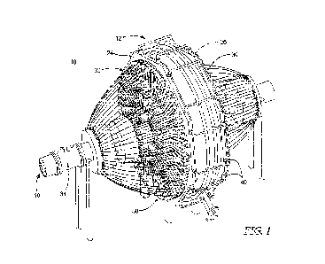
Fig. 1 is a diagram showing the primary components of one example of the solid-
state direct cavity combiner (DCC) transmitter system for providing megawatts
of power;
Fig. 2 is a diagram showing in further detail the primary components of the
solid-
state DCC transmitter system shown in Fig. 1;
Fig. 3A is a diagram showing in further detail one example of a tri-quad
module
shown in Figs. 1-2;
Fig. 3B is a diagram showing in further detail one example of the arrangement
of
two pairs of high-power transistors as a quad-module shown in Fig. 3A.
Fig. 4A shows examples of concentric ring slots located at different radii of
an
end-plate of the resonant cavity shown in one or more of Figs. 1-4;
Fig 4B shows an example of a tri-quad module shown in one or more of Figs. 1-4
inserted into concentric ring slots in the end-plate;
Fig. 5 is an interior view of the resonant cavity shown in one or more of
Figs. 1-
4B showing an example of several tri-quad modules with their respective
transmission
line and magnetic coupling loop extending through concentric ring slots shown
in Figs.
4A-4B;
Fig. 6 shows an example of a prototype of a quad module shown in one or more
of Figs. 1-5;
Fig. 7 shows an example of a prototype of a quad module shown in one or more
of Figs. 1-6;
Fig. 8 shows an example of the end-plate shown in one or more of Figs. 1-7
undergoing cooling water flow-testing;
CA 03224407 2023- 12-28
WO 2023/278669
PCT/US2022/035681
11
Fig. 9 shows an example of numerous tri-quad modules mounted on one or both
sides of the resonant cavity to provide a total of about one hundred and
twenty tri-quad
modules;
Fig. 10 is a block diagram showing the primary steps of one example of the
method for providing megawatts of power with a solid-state direct cavity
combiner (DCC)
transmitter;
Fig. 11 is a block diagram showing the primary steps of another example of the
method for providing megawatts of power with a solid-state direct cavity
combiner (DCC)
transmitter; and
Fig. 12 is a block diagram showing the primary steps of another example of the
method for providing megawatts of power with a solid-state direct cavity
combiner (DCC)
transmitter.
DETAILED DESCRIPTION OF THE INVENTION
Aside from the preferred embodiment or embodiments disclosed below, this
invention is capable of other embodiments and of being practiced or being
carried out in
various ways. Thus, it is to be understood that the invention is not limited
in its
application to the details of construction and the arrangements of components
set forth in
the following description or illustrated in the drawings. If only one
embodiment is
described herein, the claims hereof are not to be limited to that embodiment.
Moreover,
the claims hereof are not to be read restrictively unless there is clear and
convincing
evidence manifesting a certain exclusion, restriction, or disclaimer.
CA 03224407 2023- 12-28
WO 2023/278669
PCT/US2022/035681
12
There is shown in Fig. 1, one embodiment of solid-state Direct Cavity Combiner
(DCC) transmitter system 10. Solid-state DCC transmitter system 10 preferably
provides
megawatts of heating power at predetermined frequencies, including Ion
Cyclotron
Range of Frequencies (ICRF), and the like, into a demonstration or commercial
fusion
power plant. Solid-state DCC transmitter system 10 preferably provides a
reliable,
affordable, and versatile steady-state plasma heating source for commercial
fusion
generators and other technologies. The RF technology of solid-state DCC
transmitter
system 10 for plasma heating may apply to a wide range of fusion devices,
including
steady-state tokamaks and other devices.
In one example, solid-state DCC transmitter system 10 is preferably a 120 MHz
to
180 MHz 1.3 MW solid state Direct Cavity Combiner (DCC) transmitter as shown.
Solid-state DCC transmitter system 10 includes large resonant cavity 12. In
one design,
resonant cavity 12 may be about 6 feet in diameter. In other examples,
resonant cavity 12
may be smaller or larger than 6 feet in diameter, e.g., from about 6 inches to
105 inches
in diameter or similar type size. As will be discussed in detail below, solid-
state DCC
transmitter system 10 includes numerous high-power RF transistors and combines
the RF
output of the high-power RF transistors in large resonant cavity 12 preferably
operating
at about 120 MHz or similar high frequencies. Solid-state DCC transmitter
system 10
preferably combines numerous high-power RF transistors into a single resonant
cavity 12
using the subject matter disclosed in U.S. Patent No. 10,411,665 for a
Resonant Cavity
Combined Solid State Amplifier System by the applicant hereof, incorporated by
reference herein. In one design, solid-state DCC transmitter system 10 may
combine
CA 03224407 2023- 12-28
WO 2023/278669
PCT/US2022/035681
13
hundreds of high-power RF transistors into resonant cavity 12. In other
designs, Solid-
state DCC transmitter system 10 may combine more or less than hundreds of high-
power
RF transistors into resonant cavity 12. Resonant cavity 12 may operate at
higher or lower
frequencies than 120 MHz, e.g., at frequencies in the range of about 30 MHz to
about
2,400 MHz.
Solid-state DCC transmitter system 10 of one or more embodiments of this
invention addresses the modular amplifier problem with an integrated resonant
cavity 12
and hundreds of individual high-power RF transistors preferably arranged in
ordered
ranks, e.g., three concentric rows of quad modules, as discussed below. Each
transistor
module is preferably stabilized by innovative feedback control circuitry
monitoring the
drain voltage of each device and protecting the high-power RF transistors from
damage
in case of overload. Adjusting the feedback parameters of solid-state DCC
transmitter
system 10 preferably suppresses parasitic effects when solid-state DCC
transmitter
system 10 is scaled-up by a factor of 100, e.g., from about 10 kW to about
1000 kW.
Solid-state DCC transmission system 10 includes resonant cavity 12 discussed
above which includes at least one high-power transmission line output, e.g.,
high-power
transmission line 16, Fig. 2. Resonant cavity 12 is preferably configured to
provide
variable tuning and loading. System 10 also includes hundreds of high-power
transistors,
where each high-power transistor 14 generates an amount of power in the range
from 600
W to 1000 W which is input directly into resonant cavity 12. Figs. 3A, 3B, and
4B show
examples of a few high-power transistors 14 configured to provide RF power to
resonant
cavity 12, discussed in detail below.
CA 03224407 2023- 12-28
WO 2023/278669
PCT/US2022/035681
14
System 10 also includes a plurality of modules 20 which each include at least
one
pair of high-power RF transistors 14, transmission line 26, and coupling loop
28
preferably packed as module 20 as shown. In one design, each of the plurality
of modules
20 preferably include two pairs of high-power transistors 14. In other
realizations, any
integer number of pairs 22 may be combined in parallel in a module 20. Fig. 3B
shows an
example module 20 with two pairs (four) high-power transistors 14, where each
symmetric pair of high-power transistors 14 is indicated by 22. Each pair 22
of high-
power transistors 14, Figs. 3A-3B, differentially drives transmission line 26
and coupling
loop 28. Each transmission line 26 and coupling loop 28 extend into resonant
cavity 12,
Figs. 1-3A, as shown to match an impedance of each high-power transistor 14 of
each
module 20 to an impedance of resonant cavity 12 to electromagnetically couple
power
into resonant cavity 12 to provide megawatts of power to high-power output
transmission
line 16.
Each module 20 with two pairs of high-power transistor 14 is disclosed herein
as
quad module 20, e.g., four high-power transistor 14. In one example, three
quad modules
20 are preferably packed together in groups of three as tri-quad module 30 as
shown in
Fig. 3A.
Each module 20 preferably includes an overvoltage protection circuit 88, Fig.
3A
which preferably prevents damage to high-power transistors 14 in the event of
an
overload. Overvoltage protection circuit 88 is preferably configured as a
feedback
control circuit which monitors the drain voltage of each module 20 to protect
high-power
RF transistors 14 from damage in the event of an overload.
CA 03224407 2023- 12-28
WO 2023/278669
PCT/US2022/035681
The pair of high-power transistors 14 are preferably symmetrically opposed,
e.g.,
as shown in Figs. 3A and 3B, to provide differential inputs to transmission
line 26.
In one design, the plurality of modules 20, preferably as tri-quad modules 30,
are
preferably positioned on resonant cavity 12 to maximize packing density of the
high-
power transistors 14, e.g., as shown in one or more of Figs. 1-3B.
Multiple quad modules 20, e.g., tri-quad modules 30, are preferably positioned
at
different radii on end-plate 24 of resonant cavity 12, e.g., radii Ri, R2, R3,
Fig. 4A. At
least one end-plate, e.g., end-plate 24, Figs. 1-2, of resonant cavity 12,
preferably
includes a plurality of concentric ring slots 44, Fig. 4A, shown in greater
detail in Fig.
4B, which extend though end-plate 24 as shown. In one design, each
transmission line 26,
Fig. 3A, and each magnetic coupling loop 28 of each module 20 extends through
one of
the concentric ring slots 44, e.g., as shown in Figs. 4A-5.
Preferably, a plurality of modules 20, e.g., tri-quad modules 30, are
positioned
equally along concentric rings 44 about end-plate 24, e.g., as shown in Fig.
2. A plurality
of modules 20, preferably packed as tri-quad modules 30, are preferably
positioned
proximate to one or more concentric rings 44 about end-plate 24 as shown. Such
a design
maximizes packing and power density of high-power transistors 14.
Resonant cavity 12 preferably includes at least one liquid-cooled end-plate,
e.g.,
end-plate 24, Figs. 1, 2, 5 and 6 discussed above and opposing end-plate 36.
End-plate 24
preferably includes embedded water-cooling channels, exemplarily indicated at
40, Fig.
4B, which receives a cooling liquid for direct heat removal from high-power
transistors
14. In one example, each of end-plates 24, 36 is preferably a sandwich of two
copper
CA 03224407 2023- 12-28
WO 2023/278669
PCT/US2022/035681
16
plates with a labyrinth of water-cooling passages in between. The cooled end-
plates, e.g.,
end-plate 24 shown in greater detail in Fig. 5, preferably cool a majority of
the high-
power RF transistors 14 of each quad module 20 of each tri-quad module 30 as
shown
with a single cooled liquid input and output port 40. This design allows quad
modules 20
to have only three connections each (drain power 60, Figs. 6-7, gate bias
voltage 58 and
RF input 53) to operate. Only two connections may be needed if transistor bias
voltage is
derived locally from the drain power. Solid-state DCC transmitter system 10 of
one or
more embodiments of this invention preferably requires minimal ancillary
equipment
beyond an RF driver module and power supplies.
Cooling may be provided by a single input, single output water connection via
cooling ports 40 for the entire 1.3 MW resonant cavity 12.
In one example, the frequency of system 10 is in the range of about 60 MHz to
about 180 MHz. System 10 also preferably provides megawatts of power
preferably in
the range of about 1 MW to about 3 MW. In one example, the megawatts of power
provided to high-power transmission line 16. Figs. 1-2, may be used to heat
the plasma in
a fusion reactor.
In one example, each of the plurality of quad modules 20 preferably includes
an
electrostatic shield e.g., electrostatic shield 46, Fig. 5 mounted to an
interior resonant
cavity 12 to shield each magnetic coupling loop 28 from an axial field.
In one design, solid-state DCC transmitter system 10 shown in one or more of
Figs. 1-9 preferably combines four high-power RF transistors 14 as discussed
above e.g.,
900 W LDMOS transistors, or similar type transistors, into module 20 (Quad).
Each quad
CA 03224407 2023- 12-28
WO 2023/278669
PCT/US2022/035681
17
module 20 is preferably installed at different radii of cooled end-plates 24
and 36 of
resonant cavity 12 as discussed above to preferably provide for increased
power density
and low-cost, modular manufacturing. In one design, each tri-quad module 30
preferably
combines a single 600 VDC-to-50 VDC power supply, e.g., power supply 32, Fig.
3A,
with three quad modules. Power supply 32 preferably includes a single 600 VDC
input
teiminal 48 and 600 VDC to 50 VDC down converter, to provide up to 13.5 kW of
DC
power to the quad modules 20, producing 10.8 kW of RF power input to the solid-
state
DCC transmitter system 10. Power supply 32 preferably provides a constant
regulated
drain supply. Input DC current is preferably less than about 25 A.
In one example, Solid-state DCC transmitter system 10, Fig. 2, preferably
includes DC distribution subsystem 80, RF drive distribution subsystem 82,
directional
coupler subsystem 84 and high-power transmission line 16, in this example a 9-
inch
coaxial output cable.
Each quad module 20, Fig. 3A, preferably includes two-way RF power splitter
52,
including RF input connection 53 as shown, to provide RF drive to the high-
power
transistors 14. Each tri-quad module 30 preferably includes 3-way splitter 54
and RF
driver or input connection 56 as shown. Figs. 6-7 show an example of a
prototype quad
module 20 with two-way splitter 52 including RF input connection 53. The
transistor gate
bias is supplied by wire 58 and the drain power input is supplied by wire 60.
The low
output impedance of each high-power RF transistor 14 of each quad module 20 is
preferably directly connected to magnetic loop (discussed below) installed
inside the
resonant cavity 12. There are no impedance-matching transformers, circulators,
cables or
CA 03224407 2023- 12-28
WO 2023/278669
PCT/US2022/035681
18
connectors required.
The four high-power RF transistors 14, e.g., as shown in Figs. 3A-3B, of each
quad module 20 of each tri-quad module 30 are preferably mounted on a heat-
spreader 23
mounted directly to cavity end-plate 24 and/or end-plate 36 as shown in one or
more of
Figs. 1-6. Heat spreader 23 is preferably a thin plate of thermally and
electrically
conductive material (e.g. copper) which provides structural support for quad
module 20
and tri-quad module 30. As discussed above, each quad module 20, preferably
includes
magnetic coupling loop 28 extending into resonant cavity 12 via short
transmission lines
26. Magnetic coupling loop 28 preferably couples RF power to the azimuthal
magnetic
field of resonant cavity 12. In this example, each tri-quad module 30
preferably includes
three magnetic coupling loops 28, e.g., as shown in Fig. 3. Each magnetic
coupling loop
28 is preferably driven in push-pull by the four-high-power RF transistors 14,
e.g., 900 W
LDMOS RF transistors, or similar type high-power RF transistors for a total of
3.6 kW
per coupling loop, or 10.8 kW per tri-quad module 30. Each coupling loop 28
and
transmission line 26 on tri-quad module 30 may be optimized for operation in
the cavity
magnetic field at its radial position to maximize operating efficiency.
Solid-state DCC transmitter system 10 may also preferably include
electrostatic
shield, exemplarily indicated at 46, Fig. 5, mounted to the interior of
resonant cavity 12
as shown which preferably shields magnetic coupling loop 28 from the axial
electric field
within the cavity.
Fig. 7 shows an example of a prototype of a quad module 20 with four high-
power RF transistors 14, and transmission line 26 and magnetic coupling loop
28 which
CA 03224407 2023- 12-28
WO 2023/278669
PCT/US2022/035681
19
extend into resonant cavity 12. Fig. 8 shows an example of end-plate 24 shown
in one or
more of Figs. 1-7 undergoing cooling water flow-testing. In this test, a dye
is introduced
into the channel (with plexiglass covering) for visualization as shown. In
this example, at
650 MHz, a 14" (0.35 m) diameter resonant cavity 12 supports quad modules 20
as
shown. At a frequency of 120 MHz ICRF, a 75" (1.9 m) diameter resonant cavity
12 will
support about 180 quad modules per side arranged in 3 concentric rings.
In one example, a plurality of tri-quad modules 30 may be installed about
every
6 around the periphery of end-plate 24, e.g., as shown in Fig. 2. In other
examples, a
plurality of tri-quad modules 30 may be preferably installed approximately
every 6
around the periphery of end-plate 24 and/or end-plate 36, e.g., as shown in
Figs. 1 and 9.
In one example of this design, the water-cooled end-plates 24, 36 are about 72-
inch
diameter and are made of copper to serve as efficient heat sinks with a
minimum of
cooling connections.
One example of the method for providing megawatts of power with a solid-state
direct cavity combiner (DCC) transmitter includes providing a resonant cavity
including
at least one high-power output transmission line, step 100, Fig. 11. The
method also
includes providing hundreds of high-power transistors each generating an
amount of
power directly into the resonant cavity, step 102. The method also includes
providing a
plurality of modules each including at least one pair of high-power
transistors
differentially driving a transmission line and a coupling loop, step 104. The
method also
includes extending each said transmission line and coupling loop into the
resonant cavity
to the match the impedance of each said high-power transistor of each said
module to an
CA 03224407 2023- 12-28
WO 2023/278669
PCT/US2022/035681
impedance of said resonant cavity to electromagnetically couple power into the
resonant
cavity to provide megawatts of power to the high-power output transmission
line, step
106.
In another example, the method of providing megawatts of power with a solid-
state DCC transmitter includes providing a resonant cavity including at least
one high-
power output transmission line, step 110. The method also includes providing
hundreds
of high-power transistors each generating an amount of power input directly
into the
resonant cavity, step 112. The method also includes providing a plurality of
modules each
including a plurality of high-power transistors, a transmission line and a
coupling loop,
step 114. The method also includes placing the plurality of modules at
multiple different
radii on an end-plate on the resonant cavity to maximize packing density of
the high-
power transistors, step 116. The method also includes extending each
transmission line
and coupling loop into the resonant cavity to match an impedance of each said
high-
power transistor of each said module to an impedance of said resonant cavity
to
electromagnetically couple power into the resonant cavity to provide the
megawatts of
power to the high-power output transmission line, step 118.
In yet another example, the method for providing megawatts of power with a
solid-state DCC transmitter includes providing a resonant cavity including at
least one
high-power output transmission line, step 120. The method also includes
providing
hundreds of high-power transistors each generating an amount of power input
directly
into the resonant cavity, step 120. The method also includes providing a
plurality of
modules each including at least one pair of high-power transistors
differentially driving
CA 03224407 2023- 12-28
WO 2023/278669
PCT/US2022/035681
21
transmission line and a coupling loop. step 124. The method also includes
placing the
plurality of modules positioned at multiple different radii on an end-plate on
the resonant
cavity to maximize packing density of the high-power transistors, step 126.
The method
also includes extending each transmission line and coupling loop into the
resonant cavity
to match an impedance of each said high-power transistor of each said module
to an
impedance of said resonant cavity to electromagnetically couple power into the
resonant
cavity to provide the megawatts of power to the high-power output transmission
line, step
128.
The result is solid-state DCC transmitter system 10, as discussed above in one
example, preferably provides a total of about 1.3 MW of RE power when fully
populated,
e.g., about 120 tri-quad modules 60 per each end-plate 24, 36 multiplied by
three quad
modules 20 each having four high-power RF transistors each providing about 900
W.
Figs. 1 and 9 show an example of about 60 tri-quad modules 30 which each
preferably
provide about 10.8 kW of power mounted on end-plate 24 and about 60 tri-quad
modules
30 mounted on end-plate 36 such that solid-state DCC transmitter system 10 may
provide
1300 kW needed for commercial fusion reactors.
Resonant cavity 12 shown in one or more of Figs. 1-9 is preferably a linear
device
and operates similarly to a linear transformer: both are power-conserving
devices
(excepting minor losses) and superposition of magnetic and electric fields
guarantees
power output equal to power input. Thick conductive end-plates 24, 36, as
discussed
above, preferably have embedded water-cooling channels, exemplarily indicated
at 40,
Figs. 1, 2, 5 and 9, that receive a cooling liquid for direct heat removal
from high-power
CA 03224407 2023- 12-28
WO 2023/278669
PCT/US2022/035681
22
transistors 14. The cooled end-plates, e.g., end-plate 24 shown in greater
detail in Fig. 5,
preferably cool many of the high-power transistors 14 of each quad module 20
of each
tri-quad module 30 as shown with a single cooled liquid input and output port
40. This
design allows quad modules 20 to have only three connections each (drain power
60, gate
bias voltage 58 and RF input 53) to operate. Only two connectors may be needed
if bias
supplied by 58 is derived locally from the drain power. Solid-state DCC
transmitter
system 10 of one or more embodiments of this invention preferably requires
minimal
ancillary equipment beyond an RF driver module and an MVDC power supply.
Cooling may be provided by a single input, single output water connection via
cooling ports 40 for the entire 1.3 MW system 10.
The inherent high-power density of the high-power transistors, transmission
lines, and coupling loops of solid-state DCC transmitter system 10 preferably
enables a
very high-power density system which is cooled by water channels located
immediately
below the high-power RF transistors, as discussed above. The tuning of
resonant cavity
12 and output control may be performed en masse to all of the plurality of
high-power
transistors 14 by use of an axially located adjustable tuning element and an
axially
located output coupler which interact with the magnetic and electric fields
within cavity
12 to adjust its quality factor and resonant frequency. This preferably
eliminates the need
to tune each individual transistor for the system operating conditions, making
these
functions straightforward and simple. This avoids one of the problems of
conventional
commercial distributed RF systems.
Solid-state DCC transmitter system 10 preferably provides an order of
magnitude
CA 03224407 2023- 12-28
WO 2023/278669
PCT/US2022/035681
23
improvement in Mean Time Between Failures (MTBF) and Mean Time To Repair
(MTTR), preferably provides an order of magnitude reduction in physical
footprint, and
preferably provides about a 50% reduction in the cost per watt compared to
conventional
tetrode-based systems. Solid-state DCC transmitter system 10 may provide power
up to
about 1.3 MW level per resonant cavity 12 required for practical commercial
fusion
reactors.
Solid-state DCC transmitter system 10 may be mass produced with conventional
circuit fabrication techniques. The modular structure of the solid-state DCC
transmitter
system 10 discussed above may be a full-power transmitter with a partially
populated,
full-size prototype. The modular design of solid-state DCC transmitter system
10 enables
scale-up in transmitter power, easy adaptation to a range of commercial fusion
plant
configurations and sizes, and low manufacturing costs due to cost scaling of
the mass-
produced RF modules.
Together, the advantages discussed above preferably enable affordable scaling
of
this technology to the multiple megawatts of RF power required for plasma
heating in a
realistic fusion system. Solid-state DCC transmitter system 10 of one or more
embodiments of this invention may combine multiple resonant cavities 12, e.g.,
as
disclosed in the applicant's '665 patent cited supra to increase the total
available RF
power to the needs of the specific fusion system.
Every major magnetic fusion system requires auxiliary means of heating the
plasma to start the fusion reaction. ICRF heating is commonly used due to its
efficiency,
steady-state nature, and compatibility with the fusion environment. ICRF
applied to
CA 03224407 2023- 12-28
WO 2023/278669
PCT/US2022/035681
24
plasmas has shown increased plasma energy content, electron temperature and
bulk ion
heating. Heating plasmas with ICRF waves has been shown to be an effective
method of
heating present-day tokamak plasma and recent work has shown its potential to
heat
reactor plasmas. See, e.g., M J Mantsinen, et al, Analysis of Bulk Ion Heating
with ICRH
in JET High-performance Plasmas", preprint of paper Plasma Physics and
Controlled
Fusion, incorporated by reference herein.
To heat the fusion plasma, RF power in the range of 10 MW is required. A solid-
state DCC transmitter comprised of one or more embodiments of this invention
may
produce RF power in the ICRF for approximately $1/W to $2/W which is much less
than
alternative solid-state approaches or conventional tetrode-based systems.
Solid-state DCC transmitter system 10 preferably provides a modular, low-cost,
high-efficiency, high-power, highly reliable RF transmitter suitable for ICRF
fusion
plasma heating. The electrical, RF, and mechanical simplicity of the
architecture
discussed above with reference to one or more of Figs. 1-9 preferably enables
low costs
of less than $2/W, efficiencies well above 70%, total power per resonant
cavity 12 of
over 1.3 MW, with a MTBF of over 100,000 hours.
One of the primary challenges in fusion is achieving a hot dense plasma. RF
heating of fusion plasmas requires producing and controlling MWs of cost-
effective RF
power. Tetrodes are not viable for commercial fusion power, and competing
Solid-State
Amplifiers (SSAs), have a multitude of independent mechanical joints, binary
combiners,
impedance matching stages, and water coolant connections. Solid-state DCC
transmitter
system 10 of one or more embodiments of this invention uses a direct-
connection
CA 03224407 2023- 12-28
WO 2023/278669
PCT/US2022/035681
approach, which reduces costs by significantly simplifying the electrical,
thermal, and
mechanical design and also dramatically improves reliability and ease of
maintenance.
ICRF power is considered a good candidate to efficiently heat plasmas to
thermonuclear conditions for future devices like the International Tokamak
Experimental
Reactor (ITER) and the Small Prototype Advanced Robust Compact Reactor (SPARC)
has favorable scaling to reactor plasmas without core wave penetration issues.
The core
wave physics has been experimentally established including deuterium-tritium
discharges
in the Tokamak Fusion Test Reactor (TFTR) and the Joint European Tokamak
(JET).
These studies demonstrated that the majority of the power is absorbed on fuel
ions via
second harmonic tritium with co-resonant minority 3He absorption providing a
path to a
burning plasma regime. The ability to preferentially heat bulk ion, minority
ions or
electrons by an appropriate choice of the launched frequency and spectrum is
potentially
advantageous. This flexibility can be exploited to provide an effective means
of central
density and impurity control. Recent experiments in the Axially Symmetric
Divertor
Experiment Upgrade (ASDEX-U) and Alcator C-Mod shown high-power ICRF power
coupled into plasmas with minimal impurity contamination. Successful long
pulse ICRF
heating experiments show that ICRF heating technology can be used to reach
burning
plasma conditions.
Transmitter reliability is preferably increased by an order of magnitude or
more with
a solid-state RF amplifier, such as solid-state DCC transmitter system 10 of
one or more
embodiments of this invention when compared to tetrodes. Not only are
individual RF
transistors longer-lived, but the failure of an individual module has a small
impact on the
CA 03224407 2023- 12-28
WO 2023/278669
PCT/US2022/035681
26
overall operation of the amplifier; the impact being a slight reduction in
output power.
This graceful degradation means that full power operation can be maintained
even in the
event of failure of a number of modules.
An RF plant utilizing solid-state DCC transmitter system 10 would have a
dramatically longer MTBF and reduced support costs, lowering the Life Cycle
Cost
(LCC) by more than about 50%. It is estimated that solid-state DCC transmitter
system
heating transmitter will reduce the expected plant lifetime RF cost, including
tube
repair/replacements from about $4/W down to about $2.00/W, significantly
increasing
the competitiveness and feasibility of fusion power in general, and of high-
field tokamaks
in particular. One or more embodiments of solid-state DCC transmitter system
10
preferably enables smaller fusion plants by reducing the recirculating power,
which
essentially reduces a parasitic loss. 30 MW of recirculating power in a GW-
class machine
is negligible, but in a 100 MWe plant, the RF is consuming 30% of the plant
output just
to keep the plasma going. The LCC comparison is even more favorable due to the
improved efficiency of solid-state DCC transmitter system 10. Solid-state DCC
transmitter system 10 will preferably allow commercial fusion energy to meet
the
operational expectations of future utility customers.
The ability of solid-state DCC transmitter system 10 to provide reliable,
affordable, plasma heating technology makes the overall fusion system less
expensive
and simpler to operate reliably.
Direct mounting of the modules 20 on water-cooled end-plates 24 and 36
discussed above with reference to one or more of Figs. 1-9 preferably
maximizes heat
CA 03224407 2023- 12-28
WO 2023/278669
PCT/US2022/035681
27
transfer from high-power transistors 14 to the internal flow channels in end-
plates of
large resonant cavity 12 while minimizing the number of required cooling
connections
40. This preferably allows greater power density due to the ability to the
elimination of
cooling connections on the modules (enabling them to be smaller) and
dramatically
simplified maintenance requirements. Solid-state DCC transmitter system 10
provides
high transmitter reliability preferably provided by graceful degradation which
results
because each magnetic coupling loop 28, Figs. 3A, 5, and 7 has an area that is
small
compared to resonant cavity 12. Thus, even if several individual transistors
fail, their
effects only weakly couple to the cavity field and do not disrupt the
operation of solid-
state DCC transmitter system 10. The addition of more transistors than
nominally
required allows full specification performance despite any failures. Solid-
state DCC
transmitter system 10 preferably includes fast-acting DC and RF FET drain over-
voltage
protection on each quad module 20 of each of tri-quad module 30 which also
reduces risk
during operation with the inevitable plasma mismatches. Grouping the high-
power RF
transistors 14 into tri-quad-modules 30 enables increased RF power density and
simplified economical distribution of DC power.
Each quad module 20, Fig. 3A, may also preferably include a fuse configured to
isolate a shorted drain from the rest of the quad modules 20. In one example,
the fuse
may be at the 50 V drain voltage or at the 600 VDC input to the tri-quad
module down
converter 32. Future transistors may operate at higher voltages, e.g., 100 VDC
to 600
VDC, and may not need local buck converters.
Solid-state DCC transmitter system 10 preferably provides an approach to solid-
CA 03224407 2023- 12-28
WO 2023/278669
PCT/US2022/035681
28
state RF combination which is highly effective because the solid-state DCC
transmitter
system 10 allows the outputs from a large number of modules to be combined in
a single
step with minimal coupling between modules. The available power output of
solid-state
DCC transmitter system 10 of one or more embodiments of this invention is
constrained
only by the number of modules which fit on end-plates 24, 36, shown in one or
more of
Figs. 1-9.
The result is solid-state DCC transmitter system 10 discussed above preferably
provides one or more of the following key attributes which differentiate it
from other
amplifiers: low cost at MW power levels, high RF reliability and availability,
electrical,
RF. and mechanical simplicity and robustness, high efficiency operation, and
small
footprint due to high-power density of tri-quad modules.
Solid-state DCC transmitter system 10 preferably includes resonant cavity 12
that functions electrically as both a power combiner and also as an integral
part of the
transistor output matching network. Low output impedance high-power RF
transistors 14
are not matched up to an arbitrary 50-ohm impedance level. Instead, solid-
state DCC
transmitter system 10 includes magnetic coupling loops that operate at the
optimum load
impedance at the drain of the devices. This configuration is simple and has
low losses.
The resonant cavity is a well-known means of combining or dividing power.
Typically, a resonant cavity has a high unloaded Q, so that intrinsic losses
can be very
low. With heavy input and output loading, the loaded Q is much lower,
providing good
bandwidth, e.g., about 10%, while retaining the intrinsic low conduction
losses of the
cavity. Resonant cavity 12 of solid-state DCC transmitter system 10 preferably
provides a
CA 03224407 2023- 12-28
WO 2023/278669
PCT/US2022/035681
29
large, well-defined electromagnetic field structure which can be driven
simultaneously by
many transistors. Various geometry and mode combinations for resonant cavity
12 may
utilized.
The ability of resonant cavity 12 to accommodate additional high-power RF
transistors without significantly changing the interior magnetic or electric
fields by
increasing the output coupling allows nearly linear increases in power per
transistor and
simplifies each power output stage. The combination of many inputs into a
single
resonant cavity 12 provides a high degree of redundancy and a graceful
degradation
characteristic.
Resonant cavity 12 has a very high unloaded Q factor, enabling power to be
resonated out of individual amplifiers with nearly zero loss. The Q factor
drops as the
resonant cavity 12 is more heavily loaded and driven, enabling multiple
transistors to
drive resonant cavity 12 with minimal inter-module interactions. Both the
resonant
frequency and the loading of resonant cavity 12 of solid-state DCC transmitter
system 10
are preferably easily adjustable with capacitive tuning slugs, e.g. as
disclosed in the '665
patent cited supra. This allows for easy addition of Tr-Quad modules 22
without
significantly altering the internal field structure. The stability of the
internal fields
provides exceptional isolation; individual module failures do not destabilize
the resonant
cavity 12 enough to bring the solid-state DCC transmitter system 10 down and
the
remaining modules merely operate at slightly reduced power. Several
simulations were
run in Keysight Advanced Design System (ADS) and EMPro to establish the
cavity
properties under load.
CA 03224407 2023- 12-28
WO 2023/278669
PCT/US2022/035681
Based on analytical calculations and theoretical results, the applicant has
fabricated several prototype 650 MHz solid-state DCC transmitter system RF
modules
and has tested them in a 650 MHz resonant cavity 12 which demonstrated
multiple
modules combining at 2.25 kW output RF power per module, e.g., as shown in one
or
more of Figs. 1-14 and disclosed in the '665 patent cited supra.
The greatest risks of one or more embodiments solid-state DCC transmitter
system 10 of this invention may be the parasitic effects of the extreme
parameter space in
this highly engineered system. Solid-state DCC transmitter system 10 may be
characterized by its very high-power, very high-power density, and very large
mechanical
dynamic range (ratio of component size to dimensional tolerance). Parasitic
effects
occurring in electrical, RF, thermal, and mechanical domains are preferably
controlled by
one or more embodiments of solid-state DCC transmitter system 10 to ensure its
proper
operation.
Additional embodiments, designs, features, and improvements of one or more
embodiments of solid-state DCC transmitter system 10 of this invention are
disclosed in
Appendix A attached hereto.
Although specific features of the invention are shown in some drawings and not
in others, this is for convenience only as each feature may be combined with
any or all of
the other features in accordance with the invention. The words "including",
"comprising", "having", and "with" as used herein are to be interpreted
broadly and
comprehensively and are not limited to any physical interconnection. Moreover,
any
embodiments disclosed in the subject application are not to be taken as the
only possible
CA 03224407 2023- 12-28
WO 2023/278669
PCT/US2022/035681
31
embodiments. Other embodiments will occur to those skilled in the art.
What is claimed is:
CA 03224407 2023- 12-28