Note : Les descriptions sont présentées dans la langue officielle dans laquelle elles ont été soumises.
WO 2022/117894
PCT/EP2022/000024
DOPED REGION STRUCTURE AND SOLAR CELL COMPRISING THE
SAME, CELL ASSEMBLY, AND PHOTOVOLTAIC SYSTEM
TECHNICAL FIELD
[0001] The disclosure relates to the technical field of solar cells, and in
particular, to
a doped region structure and a solar cell comprising the same, a cell
assembly, and a
photovoltaic system.
BACKGROUND
[0002] Electricity generated by solar cells is a sustainable clean energy
source. By
virtue of a photovoltaic effect of a semiconductor p-n junction, sunlight can
be
converted into electric energy. Conversion efficiency is an important
indicator of the
performance of solar cells. In an interdigitated back contact (IBC) cell, a
positive/negative electrode is designed on a back side of the cell, so that a
front
surface is not at all shielded by a metal gate line, thereby completely
eradicating an
optical loss caused by the shielding of the metal gate line. In addition, a
width of the
electrode may be designed wider than a conventional electrode, so that a
series
resistance loss is reduced, thereby significantly improving the conversion
efficiency.
In addition, since the front side is designed with no electrodes, a product
has a more
beautiful appearance, and is applicable to a plurality of application
scenarios.
[0003] In a conventional passivated IBC cell with doped polysilicon, the doped
polysilicon is isolated from a silicon substrate by using a tunneling layer,
forming a
passivated contact structure in a stacked form of doped polysilicon-tunneling
layer (an
insulation layer)-silicon substrate. A thickness of the tunneling layer has a
very large
impact on a tunneling resistance. In order to form a desirable resistivity,
the thickness
of the tunneling layer is required to be small enough. However, in order to
realize a
desirable passivation effect, the thickness of the tunneling layer is required
to be large
enough. Therefore, the thickness range of the tunneling layer is required to
be strictly
1
CA 03234185 2024- 4- 8
WO 2022/117894
PCT/EP2022/000024
controlled. During production, the accuracy of the thickness of the tunneling
layer is
difficult to control. Therefore, at present, scale production is unavailable.
In addition,
requirements are also imposed for a thermal process in a follow-up production
process. Therefore, the conversion efficiency of the cell is limited.
SUMMARY
[0004] Embodiments of the disclosure are intended to provide a doped region
structure of a solar cell, to resolve the difficulty in production and the
limitation on
conversion efficiency as a result of precise requirements for a thickness of a
conventional tunneling layer.
[0005] The embodiments of the disclosure are implemented as follows. A doped
region structure of a solar cell includes
[0006] a first doped layer, a passivation layer, and a second doped layer that
are
disposed on a silicon substrate in sequence.
[0007] The passivation layer is a porous structure comprising a hole region,
and the
first doped layer and/or the second doped layer are disposed in the hole
region.
[0008] Further, the first doped layer and the second doped layer have a same
doping
polarity.
[0009] Further, a pore size of the porous structure is less than 20 gm.
[0010] Further, the pore size of the porous structure is less than 10 pm.
[0011] Further, the pore size of the porous structure is less than 1000 nm. A
hole is
designed as a nano-level hole having a pore size less than 1000 nm, and a
surface hole
density may be designed up to 106-108/cm2. It may be understood that the
arrangement of nano-level hole having the pore size less than 1000 nm greatly
reduces the overall contact area between the second doped layer and the
silicon
substrate, thereby not only reducing the resistance, but also greatly reducing
the
recombination.
2
CA 03234185 2024- 4- 8
WO 2022/117894
PCT/EP2022/000024
[0012] Further, a non-hole region of the porous structure includes a dopant
having a
same doping type as the first doped layer and/or the second doped layer.
[0013] Further, a part of the hole region of the porous structure includes the
first
doped layer and/or the second doped layer.
[0014] Further, a ratio of an area of the hole region of the porous structure
to an
entire area of the porous structure is less than 20%.
[0015] Further, a thickness of the passivation layer is in a range of 0.5-10
nm.
[0016] Further, the thickness of the passivation layer is in a range of 0.8-2
nm.
[0017] Further, the passivation layer is an oxide layer, a silicon carbide
layer, an
amorphous silicon layer, or a combination thereof.
[0018] Further, the oxide layer comprises a silicon oxide layer, an aluminum
oxide
layer, or a combination thereof.
[0019] Further, the silicon carbide layer in the passivation layer includes a
hydrogenated silicon carbide layer.
[0020] Further, a doping concentration of the first doped layer is between a
doping
concentration of the silicon substrate and a doping concentration of the
second doped
layer.
[0021] Further, a junction depth of the first doped layer is less than 1.5 gm.
[0022] Further, the first doped layer is a monocrystalline silicon doped layer
doped
with a group-Ill or group-V element.
[0023] Further, the second doped layer includes a polysilicon doped layer, a
silicon
carbide doped layer, or an amorphous silicon doped layer.
[0024] Further, the silicon carbide doped layer in the second doped layer
comprises
at least one silicon carbide doped film.
[0025] Further, the refractive indexes of the silicon carbide doped films
decrease
3
CA 03234185 2024- 4- 8
WO 2022/117894
PCT/EP2022/000024
from the silicon substrate toward outside.
[0026] Further, the silicon carbide doped layer in the second doped layer
includes a
hydrogenated silicon carbide doped layer, a conductivity of the hydrogenated
silicon
carbide doped layer is greater than 0.01 S -cm, and a thickness of the
hydrogenated
silicon carbide doped layer is greater than 10 rim.
[0027] Another embodiment of the disclosure is intended to provides a solar
cell.
The solar cell includes:
[0028] a silicon substrate;
[0029] a first doped region and a second doped region, alternately disposed on
a
back side of the silicon substrate and having opposite polarities;
[0030] a first dielectric layer, disposed on a front side of the silicon
substrate;
[0031] a second dielectric layer, disposed between the first doped region and
the
second doped region; and
[0032] a first conductive layer and a second conductive layer, respectively
disposed
in the first doped region and the second doped region.
[0033] The first doped region and/or the second doped region use(s) the doped
region structure described above.
[0034] Further, one of the first doped region and the second doped region uses
the
doped region structure described above, and the other of the first doped
region and the
second doped region is a third doped layer disposed on the back side of the
silicon
substrate.
[0035] Further, the third doped layer is a monocrystalline silicon doped layer
doped
with a group-III or group-V element.
[0036] Further, grooves spaced apart are provided on the back side of the
silicon
substrate, and the first doped region and the second doped region are
alternately
disposed in the grooves.
4
CA 03234185 2024- 4- 8
WO 2022/117894
PCT/EP2022/000024
[0037] Further, grooves spaced apart are provided on the back side of the
silicon
substrate, one of the first doped region and the second doped region is
disposed in one
of the grooves, and the other of the first doped region and the second doped
region is
disposed outside the groove.
[0038] Further, a trench is provided between the first doped region and the
second
doped region.
[0039] Further, the first doped region and/or the second doped region are/is
disposed
in a part of regions inside and outside the groove.
[0040] Further, the first dielectric layer and the second dielectric layer
each are an
aluminum oxide layer, a silicon nitride layer, a silicon oxynitride layer, a
silicon
carbide layer, an amorphous silicon layer, a silicon oxide layer, or a
combination
thereof.
[0041] Further, the first dielectric layer and/or the second dielectric layer
include(s)
the aluminum oxide layer and the silicon carbide layer, or the silicon oxide
layer and
silicon carbide layer; and
[0042] a thickness of the first dielectric layer is greater than 50 nm, and a
thickness
of the second dielectric layer is greater than 25 nm.
[0043] Further, a thickness of the aluminum oxide layer or the silicon oxide
layer in
the first dielectric layer is less than 40 nm, a thickness of the aluminum
oxide layer or
the silicon oxide layer in the second dielectric layer is less than 25 nm, and
a
thickness of the silicon carbide layer in the first dielectric layer and/or in
the second
dielectric layer is greater than 10 nm.
[0044] Further, the silicon carbide layer in the first dielectric layer and/or
in the
second dielectric layer comprises at least one silicon carbide film.
[0045] Further, the refractive indexes of the silicon carbide films decrease
from the
silicon substrate toward outside.
[0046] Further, a magnesium fluoride layer is further disposed outside the
first
CA 03234185 2024- 4- 8
WO 2022/117894
PCT/EP2022/000024
dielectric layer and/or the second dielectric layer.
[0047] Further, the first conductive layer and the second conductive layer are
TCO
transparent conductive films and/or metal electrodes_
[0048] Further, the metal electrodes each include a silver electrode, a copper
electrode, an aluminum electrode, a tin-coated copper electrode, or a silver-
coated
copper electrode.
[0049] Further, the copper electrode is electroplated copper prepared by using
an
electroplating process or the copper electrode prepared by means of physical
vapor
deposition.
[0050] Further, an electric field layer or a floating junction is disposed
between the
front side of the silicon substrate and the first dielectric layer.
[0051] Further, one of the first doped region and the second doped region is a
P-type
doped region, the other of the first doped region and the second doped region
is an N-
type doped region, and a thickness of a passivation layer in the P-type doped
region is
greater than a thickness of a passivation layer in the N-type doped region.
[0052] Further, one of the first doped region and the second doped region is a
P-type
doped region, the other of the first doped region and the second doped region
is an N-
type doped region, and a hole density of a passivation layer in the P-type
doped region
is greater than a hole density of a passivation layer in the N-type doped
region.
[0053] Another embodiment of the disclosure is intended to provides a solar
cell.
The solar cell includes:
[0054] a silicon substrate;
[0055] the doped region structure described above, disposed on a back side of
the
silicon substrate;
[0056] a third dielectric layer, disposed on the doped region structure;
[0057] a fourth doped layer and a fourth dielectric layer, disposed on a front
side of
6
CA 03234185 2024- 4- 8
WO 2022/117894
PCT/EP2022/000024
the silicon substrate in sequence; and
[0058] a third conductive layer and a fourth conductive layer, respectively
electrically connected to the doped region structure and the fourth doped
layer.
[0059] The doped region structure and the fourth doped layer have opposite
polarities.
[0060] Another embodiment of the disclosure is intended to provides a cell
assembly. The cell assembly includes one of the solar cells describe above.
[0061] Another embodiment of the disclosure is intended to provides a
photovoltaic
system. The photovoltaic system includes the cell assembly describe above.
[0062] Another embodiment of the disclosure is intended to provides a cell
assembly. The cell assembly includes another of the solar cells describe
above.
[0063] Another embodiment of the disclosure is intended to provides a
photovoltaic
system. The photovoltaic system includes another of the cell assemblies
describe
above.
[0064] Different from the passivated contact structure in the prior art,
according to
the doped region structure of the solar cell provided in the embodiments of
the
disclosure, the first doped layer, the passivation layer, and the second doped
layer are
disposed in sequence, the passivation layer is arranged as a porous structure,
and the
hole region has the first doped layer and/or the second doped layer.
Therefore, a
conductive channel is formed in the hole region of the passivation layer, so
that a
desirable resistivity of the passivation layer is formed. In this way, a
thickness of the
passivation layer has a less impact on the resistance, and the control
requirements for
the thickness of the passivation layer are lowered. Thus, more methods are
applicable
to preparation of the passivation layer compared with the prior art. In an
embodiment,
the hole is designed as a nano-level hole having a pore size less than 1000
nm, so that
the surface hole density is as high as 106-108/em2. It may be understood that
the
arrangement of nano-level hole having the pore size less than 1000 nm greatly
7
CA 03234185 2024- 4- 8
WO 2022/117894
PCT/EP2022/000024
reduces the overall contact area between the second doped layer and the
silicon
substrate, thereby not only reducing the resistance, but also greatly reducing
the
recombination. The first doped layer is disposed between the silicon substrate
and the
passivation layer to form a separation electric field capable of enhancing
surface
electron holes, so that the field passivation effect is enhanced. Since a
Fermi level of
the first doped layer is different from a Fermi level of the silicon
substrate, the Fermi
level of the first doped layer is changed. A solid concentration of impurities
(transition
metals) is increased, so that an additional impurity gettering effect is
achieved. In
addition, in the porous structure, the second doped layer is connected to the
silicon
substrate through the doped hole region and the first doped layer, so that the
overall
resistance of the prepared cell is further reduced, and the conversion
efficiency of the
cell is improved. In this way, the difficulty in production and the limitation
on the
conversion efficiency as a result of precise requirements for the thickness of
the
conventional tunneling layer are resolved.
BRIEF DESCRIPTION OF THE DRAWINGS
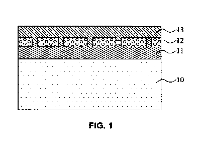
[0065] FIG. 1 is a schematic structural diagram of a doped region structure of
a solar
cell according to an embodiment of the disclosure.
[0066] FIG. 2 to FIG. 8 are schematic structural diagrams of a solar cell
during
various implementation according to an embodiment of the disclosure.
[0067] FIG. 9 is a schematic structural diagram of a solar cell according to
another
embodiment of the disclosure.
DETAILED DESCRIPTION
[0068] To make the objectives, technical solutions and advantages of the
disclosure
clearer and more comprehensible, the disclosure is further described in detail
below
with reference to the accompanying drawings and embodiments. It is to be
understood
that the specific embodiments described herein are merely used to explain the
8
CA 03234185 2024- 4- 8
WO 2022/117894
PCT/EP2022/000024
disclosure, but are not intended to limit the disclosure.
[0069] In the disclosure, unless otherwise explicitly specified or defined,
the terms
such as "mount", "install", "connect", "connection", and "fix" should be
understood
in a broad sense. For example, the connection may be a fixed connection, a
detachable
connection, or an integral connection; or the connection may be a mechanical
connection or an electrical connection; or the connection may be a direct
connection,
an indirect connection through an intermediary, or internal communication
between
two components. A person of ordinary skill in the art may understand specific
meanings of the foregoing terms in the disclosure according to specific
situations. The
term "and/or" used in this specification includes any and all combinations of
one or
more related listed items.
[0070] Different from the passivated contact structure in the prior art, in
the
disclosure, a first doped layer, a passivation layer, and a second doped layer
are
disposed in sequence, the passivation layer is arranged as a porous structure,
and a
hole region has the first doped layer and/or the second doped layer.
Therefore, a
conductive channel is formed in the hole region of the passivation layer, so
that a
desirable resistivity of the passivation layer is formed. In this way, a
thickness of the
passivation layer has a less impact on the resistance, and the control
requirements for
the thickness of the passivation layer are lowered. Thus, more methods are
applicable
to preparation of the passivation layer compared with the prior art. The first
doped
layer is disposed between the silicon substrate and the passivation layer to
form a
separation electric field capable of enhancing surface electron holes, so that
the field
passivation effect is enhanced. Since a Fermi level of the first doped layer
is different
from a Fermi level of the silicon substrate, the Fermi level of the first
doped layer is
changed. A solid concentration of impurities (transition metals) is increased,
so that an
additional impurity gettering effect is achieved. In addition, in the porous
structure,
the second doped layer is connected to the silicon substrate through the doped
hole
region and the first doped layer, so that the overall resistance of the
prepared cell is
further reduced, and the conversion efficiency of the cell is improved. In
this way, the
9
CA 03234185 2024- 4- 8
WO 2022/117894
PCT/EP2022/000024
difficulty in production and the limitation on the conversion efficiency as a
result of
precise requirements for the thickness of the conventional tunneling layer are
resolved.
Example 1
[0071] An embodiment of the disclosure provides a doped region structure of a
solar
cell. For ease of description, only parts related to this embodiment of the
disclosure
are shown. Referring to FIG. 1, the doped region structure of the solar cell
provided in
this embodiment of the disclosure includes:
[0072] a first doped layer 11, a passivation layer 12, and a second doped
layer 13
that are disposed on a silicon substrate 10 in sequence.
[0073] The passivation layer 12 is a porous structure having the first doped
layer 11
and/or the second doped layer 13 in a hole region.
[0074] In an embodiment of the disclosure, the silicon substrate 10 has a
front side
facing the sun during normal operation and a back side opposite to the front
side. The
front side is a light-receiving surface. The back side is opposite to the
front side and
disposed on an other side of the silicon substrate 10. That is to say, the
front side and
the back side are located on different and opposite sides of the silicon
substrate 10. In
this embodiment, the silicon substrate 10 is an N-type monocrystalline silicon
wafer.
It may be understood that, in other embodiments, the silicon substrate 10 may
also be
silicon wafers of other types, such as a polysilicon wafer, a quasi-
monocrystalline
silicon wafer, or the like. The silicon substrate 10 may also be designed as a
P type.
The silicon substrate 10 may be designed according to actual use requirements,
which
is not specifically limited herein.
[0075] In an embodiment of the disclosure, the passivation layer 12 is
preferably an
oxide layer, a silicon carbide layer, an amorphous silicon layer, or a
combination
thereof. In some examples of the disclosure, the passivation layer 12 may
include a
single material such as an oxide layer, a plurality of types of materials such
as a
CA 03234185 2024- 4- 8
WO 2022/117894
PCT/EP2022/000024
combination of an oxide layer and an amorphous silicon layer, or a single
material
such as a combination of a plurality of amorphous silicon layers each having a
specific refractive index. In addition, the first passivation layer 12 may
also be a
silicon oxynitride layer, a silicon nitride layer, or the like. It may be
understood that,
the specific structure of the passivation layer 12 includes but is not limited
to the
above. The passivation layer 12 may be correspondingly designed according to
actual
use requirements, which is not specifically limited herein. Further, a
thickness of the
passivation layer 12 is in a range of 0.5-10 nm. In a preferable embodiment of
the
disclosure, the thickness of the passivation layer 12 is in a range of 0.8-2
nm. The
thickness of the passivation layer 12 may be designed as a thickness of a
tunneling
layer in the prior art or a thickness larger than the thickness of the
conventional
tunneling layer. The thickness may be designed according to actual use
requirements,
which is not specifically limited herein.
[0076] In a preferable embodiment of the disclosure, specifically, the
passivation
layer 12 includes the oxide layer and the silicon carbide layer. The oxide
layer and the
silicon carbide layer are arranged in sequence from the silicon substrate 10
toward
outside. The oxide layer is in contact with the first doped layer 11 located
inside, and
the silicon carbide layer is in contact with the second doped layer 13 located
outside.
Further, the oxide layer preferably comprises a silicon oxide layer, an
aluminum oxide
layer, or a combination thereof. Therefore, the passivation layer 12 may also
be a
combination of the silicon oxide layer and the aluminum oxide layer in the
oxide
layer. The silicon carbide layer in the passivation layer 12 includes a
hydrogenated
silicon carbide layer. Hydrogen in the hydrogenated silicon carbide layer
enters the
silicon substrate 10 under a diffusion mechanism and a thermal effect, so that
a
dangling bond for neutralizing the back side of the silicon substrate 10
passivates
defects of the silicon substrate 10. Therefore, mitigating dangling bonds in a
forbidden band increases the probability that a carrier enters the second
doped layer
13 through the passivation layer 12.
[0077] Further, in an embodiment of the disclosure, the passivation layer 12
is a
11
CA 03234185 2024- 4- 8
WO 2022/117894
PCT/EP2022/000024
porous structure. The porous structure may be prepared by means of additional
chemical corrosion, dry etching, or thermal diffusion impact, or the like. The
porous
structure is performed according to actual use requirements, which is not
specifically
limited herein. It should be noted that, the porous structure is in a top view
of the
passivation layer 12. In a cross-sectional view of the passivation layer 12, a
multi-
channel structure is shown. The porous structure has holes extending through
the
passivation layer 12. The porous structure also has grooves/openings not
extending
through the passivation layer 12 on a surface of the passivation layer 12. A
pore size
of the porous structure is less than 20 p.m. Specifically, an average pore
size of the
holes is less than 20 pm, or pore sizes of 90% of all of the holes are less
than 2011M.
Further, the pore size of the porous structure is less than 10 tun. Further,
the pore size
of the porous structure is less than 1000 nm. In this case, a hole is designed
as a nano-
level hole having a pore size less than 1000 nm, and a surface hole density
may be
designed up to 106-108/cm2. It may be understood that the arrangement of nano-
level
hole having the pore size less than 1000 nm greatly reduces the overall
contact area
between the second doped layer and the silicon substrate, thereby not only
reducing
the resistance, but also greatly reducing the recombination. A ratio of an
area of the
hole region of the porous structure to an entire area of the porous structure
is less than
20%, that is, the holes are sparsely distributed on the passivation layer 12.
[0078] In an embodiment of the disclosure, the hole region of the porous
structure
includes the first doped layer 11 and/or the second doped layer 13. That is to
say, the
hole region may be inlaid with the first doped layer 11 or the second doped
layer 13
alone, or may be inlaid with a mixture of the first doped layer 11 and the
second
doped layer 13. It needs to be noted that, in an actual production and
preparation
process, a part of the hole region of the porous structure may include the
first doped
layer 11 and/or the second doped layer 13, and other parts that are not filled
with the
first doped layer 11 and/or the second doped layer 13 are gap regions. It
needs to be
further noted that, in addition to the first doped layer 11 and/or the second
doped layer
13 filled in the hole region, impurities (such as hydrogen, oxygen, and
various metal
12
CA 03234185 2024- 4- 8
WO 2022/117894
PCT/EP2022/000024
elements) formed in a thermal process (the production of solar cells may
include a
plurality of high temperature processes according to different processes) or
generated
during segregation are allowed to exist in the hole region.
[0079] Further, in an embodiment of the disclosure, a non-hole region of the
porous
structure includes a dopant having a same doping type as the first doped layer
11
and/or the second doped layer 13. For example, when the first doped layer 11
and the
second doped layer 13 are N-type doped layers (such as a phosphorus doped
layer),
the non-hole region of the passivation layer 12 includes a diffused N-type
dopant.
[0080] In an embodiment of the disclosure, the first doped layer 11 is located
between the silicon substrate 10 and the passivation layer 12. The first doped
layer 11
may be a doped layer directly formed on the silicon substrate 10 by means of
ion
implantation or the like. In this case, the first doped layer 11 is located on
the silicon
substrate 10. Correspondingly, the passivation layer 12 is prepared on the
first doped
layer 11. The first doped layer 11 may also be a doped layer formed on the
silicon
substrate 10 after a doping source directly penetrates the passivation layer
12 or the
holes in the porous structure during preparation of the second doped layer 13.
In this
case, the first doped layer 11 is located in the silicon substrate 10.
Correspondingly,
the passivation layer 12 is directly prepared on the silicon substrate 10.
Therefore,
during the preparation of the second doped layer 13, the passivation layer is
thermally
diffused into the silicon substrate 10, so that a part of the silicon
substrate 10 is
transformed into the first doped layer 11 through diffusion. A doping
concentration of
the first doped layer 11 is between a doping concentration of the silicon
substrate 10
and a doping concentration of the second doped layer 13. In a preferred
embodiment
of the disclosure, the first doped layer 11 and the second doped layer 13 have
a same
doping polarity. For example, when the second doped layer 13 is an N-type
doped
layer, the first doped layer 11 is correspondingly preferably an N-type doped
layer. It
needs to be noted that, the doping polarities of the first doped layer 11 and
the second
doped layer 13 may be different from a doping polarity of the silicon
substrate 10. For
example, in this embodiment, the silicon substrate 10 is an N-type
monocrystalline
13
CA 03234185 2024- 4- 8
WO 2022/117894
PCT/EP2022/000024
silicon, and the first doped layer 11 and the second doped layer 13 may be P-
type
doped layers.
[0081] Preferably, a material of the first doped layer 11 is preferably
designed as
same as the silicon substrate 10. That is to say, when the silicon substrate
10 is a
monocrystalline silicon wafer, the first doped layer 11 is also preferably
designed as
the monocrystalline silicon wafer. The first doped layer 11 is a
monocrystalline silicon
doped layer doped with a group-HI or group-V element. When the second doped
layer
13 is the N-type doped layer, the first doped layer 11 is a monocrystalline
silicon
doped layer doped with group-V elements such as nitrogen, phosphorus, and
arsenic.
When the second doped layer 13 is the P-type doped layer, the first doped
layer 11 is a
monocrystalline silicon doped layer doped with group-III elements such as
boron,
aluminum, and gallium. It may be understood that, when the silicon substrate
10 is
designed as silicon wafers of other types, the first doped layer 11 may also
be
correspondingly designed as doped silicon wafers of other types doped with a
group-
III or group-V element.
[0082] Further, in an embodiment of the disclosure, the first doped layer 11
is in a
discrete or continuous distribution. The first doped layer may be completely
continuously disposed between the silicon substrate 10 and the passivation
layer 12,
or locally discretely distributed near each hole region of the passivation
layer 12. The
distribution of the first doped layer 11 may be controlled by using a doping
process. A
doping amount increases over a doping time, so that the first doped layer 11
is more
continuous, until the first doped layer 11 fully covering the silicon
substrate 10 is
formed thereon. Further, a junction depth of the first doped layer 11 is less
than 1.5
gm.
[0083] In an embodiment of the disclosure, the second doped layer 13 includes
a
polysilicon doped layer, a silicon carbide doped layer, or an amorphous
silicon doped
layer. The silicon carbide doped layer in the second doped layer 13 comprises
at least
one silicon carbide doped film each having a specific refractive index. The
refractive
indexes of the silicon carbide doped films decrease from the silicon substrate
10
14
CA 03234185 2024- 4- 8
WO 2022/117894
PCT/EP2022/000024
toward the outside. It needs to be noted that, thicknesses and the refractive
indexes of
the silicon carbide doped films may be designed according to actual use
requirements,
provided that the refractive indexes decrease from the silicon substrate 10
toward the
outside, which are not specifically limited herein. Since silicon carbide has
a wide
optical band gap and a low absorption coefficient, parasitic absorption can be
reduced,
and a short-circuit current density can be effectively increased. Further, the
silicon
carbide doped layer in the second doped layer 13 includes a hydrogenated
silicon
carbide doped layer. A conductivity of the hydrogenated silicon carbide doped
layer is
greater than 0.01 S =cm, and a thickness of the hydrogenated silicon carbide
doped
layer is greater than 10 nm. Correspondingly, the conductivity and the
thickness may
also be set to other values, provided that a requirement for the of the second
doped
layer 13 can be met by controlling the conductivity and the thickness of the
hydrogenated silicon carbide doped layer, which are not specifically limited
herein. It
needs to be noted that, the first doped layer 11 and the second doped layer 13
may
have a same material or different materials. For example, the first doped
layer 11 and
the second doped layer 13 both include doped polysilicon. Alternatively, the
first
doped layer 11 may include doped monocrystalline silicon, and the second doped
layer 13 may include doped silicon carbide.
[0084] Different from the passivated contact structure in the prior art, in
this
embodiment, the first doped layer, the passivation layer, and the second doped
layer
are disposed in sequence, the passivation layer is arranged as a porous
structure, and
the hole region has the first doped layer and/or the second doped layer.
Therefore, a
conductive channel is formed in the hole region of the passivation layer, so
that a
desirable resistivity of the passivation layer is formed. In this way, a
thickness of the
passivation layer has a less impact on the resistance, and the control
requirements for
the thickness of the passivation layer are lowered. Thus, more methods are
applicable
to preparation of the passivation layer compared with the prior art. The first
doped
layer is disposed between the silicon substrate and the passivation layer to
form a
separation electric field capable of enhancing surface electron holes, so that
the field
CA 03234185 2024- 4- 8
WO 2022/117894
PCT/EP2022/000024
passivation effect is enhanced. Since a Fermi level of the first doped layer
is different
from a Fermi level of the silicon substrate, the Fermi level of the first
doped layer is
changed. A solid concentration of impurities (transition metals) is increased,
so that an
additional impurity absorption effect is achieved. In addition, in the porous
structure,
the second doped layer is connected to the silicon substrate through the doped
hole
region and the first doped layer, so that the overall resistance of the
prepared cell is
further reduced, and the conversion efficiency of the cell is improved. In
this way, the
difficulty in production and the limitation on the conversion efficiency as a
result of
precise requirements for the thickness of the conventional tunneling layer are
resolved.
Example 2
[0085] A second embodiment of the disclosure provides a solar cell. For ease
of
description, only parts related to this embodiment of the disclosure are
shown.
Referring to FIG. 2 to FIG. 8, the solar cell provided in this embodiment of
the
disclosure includes:
[0086] a silicon substrate 10;
[0087] a first doped region 20 and a second doped region 30, alternately
disposed on
a back side of the silicon substrate 10 and having opposite polarities;
[0088] a first dielectric layer 40, disposed on a front side of the silicon
substrate 10;
[0089] a second dielectric layer 50, disposed between the first doped region
20 and
the second doped region 30; and
[0090] a first conductive layer 60 and a second conductive layer 70,
respectively
disposed in the first doped region 20 and the second doped region 30.
[0091] The first doped region 20 and/or the second doped region 30 use(s) the
doped
region structure described in the above embodiments.
[0092] Thus, in an embodiment of the disclosure, the first doped region 20 and
the
16
CA 03234185 2024- 4- 8
WO 2022/117894
PCT/EP2022/000024
second doped region 30 in the solar cell both may use the doped region
structure
described in the above embodiments. Referring to FIG. 2, FIG. 4, and FIG. 6,
since
the first doped region 20 and the second doped region 30 have opposite
polarities, a
first doped layer and a second doped layer in the first doped region 20 and a
first
doped layer and a second doped layer in the second doped region 30 also have
opposite polarities. For example, when the first doped layer and the second
doped
layer in the first doped region 20 are P-type doped layers, the first doped
layer and the
second doped layer in the second doped region 30 are N-type doped layers
having
opposite doping polarities. In this case, the first doped region 20 is a P-
type doped
region, and the second doped region 30 is an N-type doped region. Definitely,
the first
doped region 20 may also be the N-type doped region, and the second doped
region
30 may also be the P-type doped region. Therefore, when one of the first doped
region
20 and the second doped region 30 is the P-type doped region, the other of the
first
doped region and the second doped region is the N-type doped region.
[0093] Defmitely, alternatively, one of the first doped region 20 and the
second
doped region 30 in the solar cell uses the doped region structure described in
the
above embodiments, and the other of the first doped region and the second
doped
region uses a conventional structure (such as a passivated contact structure
or a
diffusion structure). In this embodiment, preferably, the other one is a third
doped
layer disposed in the back side of the silicon substrate 10. That is to say,
the other one
uses the conventional diffusion structure, as shown in FIG. 3, FIG. 5, FIG. 7,
and FIG.
8. Definitely, optionally, the other one may also use the conventional
passivated
contact structure. The passivated contact structure includes a tunneling layer
and a
doped region (not shown in the figure). It needs to be noted that, the third
doped layer
is also a monocrystalline silicon doped layer doped with a group-HI or group-V
element. For a specific structure of the third doped layer, refer to the
description of the
first doped layer in the above embodiments. It needs to be further noted that,
since the
first doped region 20 and the second doped region 30 have opposite polarities,
and the
first doped layer and the second doped layer have the same doping polarity,
the first
17
CA 03234185 2024- 4- 8
WO 2022/117894
PCT/EP2022/000024
doped layer and the third doped layer are respectively doped with an element
of a
different group. That is to say, when the first doped layer is doped with a
group-III
element, the third doped layer is doped with a group-V element. When the first
doped
layer is doped with a group-V element, the third doped layer is doped with a
group-III
element.
[0094] When the first doped region 20 and the second doped region 30 both use
the
doped region structure described in the above embodiments, a material and a
thickness selected for each layer structure in the first doped region 20 may
be same as
or different from those selected for each layer structure in the second doped
region 30.
For example, when a passivation layer in the first doped region 20 is
specifically
selected as a silicon oxide layer and a silicon carbide layer, a passivation
layer in the
second doped region 30 may be selected to be the same as the passivation layer
in the
first doped region 20, or may be selected as a material different from the
passivation
layer in the first doped region 20, such as an aluminum oxide layer and a
silicon
carbide layer.
[0095] A thickness of the passivation layer in the first doped region 20 may
be
designed same as or different from a thickness of the passivation layer in the
second
doped region 30. Preferably, regardless of whether the material of the
passivation
layer in the first doped region 20 is the same as the material of the
passivation layer in
the second doped region 30, the thickness of the passivation layer
corresponding to
the first doped layer doped with the group-III element is designed to be
larger, and the
thickness of the passivation layer corresponding to the first doped layer
doped with
the group-V element is designed to be smaller. That is to say, the thickness
of the
passivation layer in the P-type doped region is greater than the thickness of
the
passivation layer in the N-type doped region. A main reason lies in that the P-
type
doped region requires a process such as boron doping and a higher temperature,
and
requires a thicker passivation layer due to a requirement for a plurality of
heat
treatment processes. In this embodiment, the material and the thickness of
each layer
structure in the first doped region 20 and in the second doped region 30 are
18
CA 03234185 2024- 4- 8
WO 2022/117894
PCT/EP2022/000024
correspondingly designed according to actual use requirements, which are not
specifically limited herein.
[0096] In addition, in a preferred embodiment of the disclosure, a hole
density of the
passivation layer in the P-type doped region is greater than a hole density of
the
passivation layer in the N-type doped region. The hole density means a
quantity of
holes per unit area. That is to say, in a same unit area, the passivation
layer in the P-
type doped region has more holes than the passivation layer in the N-type
doped
region. A main reason lies in that a conductivity of the P-type doped region
is
relatively poor, and the thickness of the passivation layer in the P type
doped region is
relatively large. Therefore, more holes are required to enhance the
conductivity.
[0097] In an embodiment of the disclosure, the first dielectric layer 40 and
the
second dielectric layer 50 each are an aluminum oxide layer, a silicon nitride
layer, a
silicon oxynitride layer, a silicon carbide layer, an amorphous silicon layer,
a silicon
oxide layer, or a combination thereof. The first dielectric layer 40 and the
second
dielectric layer 50 achieve a passivation effect. The first dielectric layer
40 and the
second dielectric layer 50 each are designed as a structure having at least
one layer.
Refractive indexes of the first dielectric layer and the second dielectric
layer decrease
from the silicon substrate 10 toward the outside, so that a film layer close
to the
silicon substrate 10 achieves the passivation effect, and a film layer away
from the
silicon substrate 10 achieves an antireflection effect, thereby enhancing the
anti-
reflection effect. In this way, the silicon substrate 10 absorbs and uses
light more
effectively, and the short-circuit current density is increased. Each film
layer in the
first dielectric layer 40 and in the second dielectric layer 50 that has a
different
structure comprises a plurality of films each having a specific refractive
index.
According to the above, the film layers are arranged such that the refractive
indexes
of the film layers decrease from the silicon substrate 10 toward the outside.
For
example, the silicon oxide layer in the first dielectric layer 40 comprises a
plurality of
silicon oxide films having refractive indexes decreasing from the silicon
substrate 10
toward the outside.
19
CA 03234185 2024- 4- 8
WO 2022/117894
PCT/EP2022/000024
[0098] It should be noted that, the first dielectric layer 40 and the second
dielectric
layer 50 may have a same structural arrangement or different structural
arrangements.
The film layer structures in the first dielectric layer 40 and in the second
dielectric
layer 50 may be correspondingly designed according to actual use requirements,
which are not specifically limited herein. Preferably, the first dielectric
layer 40 and
the second dielectric layer 50 are designed same, so that the first dielectric
layer 40
and the second dielectric layer 50 may be prepared on the front side and the
back side
of the silicon substrate 10 respectively by using a same process.
[0099] In a preferred embodiment of the disclosure, the first dielectric layer
40
and/or the second dielectric layer 50 include/includes a double-layer
structure of an
aluminum oxide layer and a silicon carbide layer or a double-layer structure
of a
silicon oxide layer and a silicon carbide layer. In this case, an entire
thickness of the
first dielectric layer 40 is greater than 50 nm, and an entire thickness of
the second
dielectric layer 50 is greater than 25 nm. It may be understood that, the
specific
structural arrangements of the first dielectric layer 40 and the second
dielectric layer
50 include but are not limited to the specific examples listed above.
[0100] Further, in an embodiment of the disclosure, a thickness of the
aluminum
oxide layer or the silicon oxide layer in the first dielectric layer 40 is
less than 40 am.
A thickness of the aluminum oxide layer or the silicon oxide layer in the
second
dielectric layer 50 is less than 25 nm. A thickness of the silicon carbide
layer in the
first dielectric layer 40 and/or in the second dielectric layer 50 is greater
than 10 nm.
The silicon carbide layer in the first dielectric layer 40 and/or in the
second dielectric
layer 50 can not only provide a hydrogen passivation effect, but also reduce
parasitic
light absorption by virtue of a large optical band gap and a small absorption
coefficient.
[0101] It needs to be noted that, the multi-layer structure in this embodiment
of the
disclosure conforms to an arrangement sequence from the silicon substrate 10
toward
the outside. For example, when the above first dielectric layer 40 includes
the
aluminum oxide layer and the silicon carbide layer, the aluminum oxide layer
is close
CA 03234185 2024- 4- 8
WO 2022/117894
PCT/EP2022/000024
to the silicon substrate 10, and the silicon carbide layer is close to the
outside. It needs
to be further noted that, in the drawings, FIG. 2 to FIG. 8 only show the
first dielectric
layer 40 and the second dielectric layer 50 as double-layer structures.
However, it may
be understood that, the first dielectric layer 40 and the second dielectric
layer 50 may
also include other quantities of layers. Respective specific structures may be
designed
according to actual needs, and are not completely limited to the drawings. It
needs to
be further noted that, each drawing of the disclosure is merely used to
describe the
specific structural distribution in the solar cell, but does not correspond to
an actual
size of each structure. The drawings do not completely correspond to specific
actual
sizes in this embodiment, and the actual size of each structure needs to
conform to
specific parameters provided in this embodiment_
[0102] Further, the silicon carbide layer in the first dielectric layer 40
and/or in the
second dielectric layer 50 comprises at least one silicon carbide film. The
refractive
indexes of the silicon carbide films decrease from the silicon substrate 10
toward the
outside. Optionally, the refractive indexes of the above material may be
generally
selected as follows: the refractive index of monocrystalline silicon is 3.88,
the
refractive index of amorphous silicon is in a range of 3.5-4.2, the refractive
index of
polysilicon is 3.93, the refractive index of silicon carbide is in a range of
2-3.88, the
refractive index of silicon nitride is in a range of 1.9-3.88, the refractive
index of
silicon oxynitride is in a range of 1.45-3.88, the refractive index of silicon
oxide is
1.45, and the refractive index of aluminum oxide is 1.63. It may be understood
that,
the refractive indexes of the above materials may also be set to other values
according
to actual use requirements, which are not specifically limited herein.
[0103] Further, in an embodiment of the disclosure, a magnesium fluoride layer
is
further disposed outside the first dielectric layer 40 and/or the second
dielectric layer
50. That is to say, in addition to one or a combination of more of the
aluminum oxide
layer, the silicon nitride layer, the silicon oxynitride layer, the silicon
carbide layer,
the amorphous silicon layer, and the silicon oxide layer selected for the
first dielectric
layer 40 and the second dielectric layer 50, a magnesium fluoride layer may be
further
21
CA 03234185 2024- 4- 8
WO 2022/117894
PCT/EP2022/000024
disposed outside the first dielectric layer 40 and/or the second dielectric
layer 50. The
magnesium fluoride layer is required to have a lowest refractive index.
Generally, the
refractive index is set to 1.4. The magnesium fluoride layer has an optical
effect of
enhancing antireflection.
[0104] Further, in an embodiment of the disclosure, an electric field layer or
a
floating junction is disposed between the front side of the silicon substrate
10 and the
first dielectric layer 40. Specifically, the electric field layer is prepared
by means of
phosphorus diffusion on the silicon substrate 10, or the floating junction is
prepared
by means of boron diffusion. The electric field layer or the floating junction
is used as
a front surface electric field of the solar cell.
[0105] In an embodiment of the disclosure, the first conductive layer 60
and/or the
second conductive layer 70 are/is a TCO transparent conductive film and/or a
metal
electrode. The metal electrode includes a silver electrode, a copper
electrode, an
aluminum electrode, a tin-coated copper electrode, or a silver-coated copper
electrode.
Further, the copper electrode is electroplated copper prepared by using an
electroplating process or the copper electrode prepared by means of physical
vapor
deposition. A nickel electrode, a chromium electrode, a titanium electrode, or
a
tungsten electrode is used as a seed layer or a protective layer of the
electroplated
copper. It needs to be noted that, the first conductive layer 60 and the
second
conductive layer 70 may select a same electrode or different electrodes. For
example,
the first conductive layer 60 and the second conductive layer 70 both select
the
aluminum electrode. Alternatively, the first conductive layer 60 selects the
silver
electrode, and the second conductive layer 70 selects the aluminum electrode.
[0106] Further, in an embodiment of the disclosure, a texturing process is
further
performed before the first dielectric layer 40 is prepared on the front side
of the
silicon substrate 10. A shape formed on the front side includes but is not
limited to an
alkali polished surface, a mechanically polished surface, a random pyramid
shape, an
inverted pyramid shape, a spherical cap shape, a V-shaped groove, and a shape
ranging among the above shapes. The surface shape formed on the front side of
the
22
CA 03234185 2024- 4- 8
WO 2022/117894
PCT/EP2022/000024
silicon substrate 10 helps reduce the reflection of sunlight on the front
side, thereby
improving the conversion efficiency of the solar cell.
[0107] Further, in an embodiment of the disclosure, the second dielectric
layer 50
may cover only a region between the first doped region 20 and the second doped
region 30 on the silicon substrate 10, or may extend to cover the first doped
region 20
and/or the second doped region 30. When the second dielectric layer 50 covers
only
the region between the first doped region 20 and the second doped region 30 on
the
silicon substrate 10, the first conductive layer 60 covers an entire back side
of the first
doped region 20 for electric connection, and the second conductive layer 70
covers an
entire back side of the second doped region 30 for electric connection. When
the
second dielectric layer 50 extends to cover the first doped region 20 and/or
the second
doped region 30, the first conductive layer 60 covers a back surface of a
remaining
part that not covered by the second dielectric layer 50 in the first doped
region 20 for
achieve electric connection, and the second conductive layer 70 covers a back
surface
of a remaining part not covered by the second dielectric layer 50 in the
second doped
region 30 for electric connection. When the second dielectric layer 50 covers
the
entire back side, the first conductive layer 60 penetrates the second
dielectric layer 50
through perforations or the like to be electrically connected to the first
doped region
20, and the second conductive layer 70 penetrates the second dielectric layer
50
through perforations or the like to be electrically connected to the second
doped
region 30. The conductive polarities of the first conductive layer 60 and the
second
conductive layer 70 are determined according to the polarities of the first
doped
region 20 and the second doped region 30, which are not specifically limited
herein.
[0108] In an embodiment of the disclosure, referring to FIG. 2 and FIG. 3, the
first
doped region 20 and the second doped region 30 are alternately disposed on the
back
side of the silicon substrate 10. In order to avoid undesirable phenomena such
as
electric leakage caused by unobstructed connection between the first doped
region 20
and the second doped region 30, a trench is provided between the first doped
region
20 and the second doped region 30. The trench separates the first doped region
20
23
CA 03234185 2024- 4- 8
WO 2022/117894
PCT/EP2022/000024
from the second doped region 30. Correspondingly, the second dielectric layer
50
covers the trench. It needs to be noted that, a surface shape of the trench
that is in
contact with the silicon substrate 10 may further have a rough texture
structure
disposed thereon_ The rough texture structure is usually formed by means of
texturing,
and includes but is not limited to an alkali polished surface, a mechanically
polished
surface, a random pyramid shape, an inverted pyramid shape, a spherical cap
shape, a
V-shaped groove, and a shape ranging among the above shapes. An irregular
hemispherical texture may be formed by means of acid texturing, a pyramid-
shaped
texture may be formed by means of alkali texturing, or the pyramid-shaped
texture
may be formed first by means of alkali texturing and then smoothing is
performed on
a top of a pyramid-shaped by means of acid texturing. In this way, the surface
shape
formed at the trench on the back side of the silicon substrate 10 helps the
silicon
substrate 10 absorb and reuse light more effectively, and the short-circuit
current
density is increased, thereby enhancing the conversion efficiency of the solar
cell.
[0109] In another embodiment of the disclosure, referring to FIG. 4 and FIG.
5,
grooves spaced apart are provided on the back side of the silicon substrate
10. The
first doped region 20 and the second doped region 30 are alternately disposed
in the
grooves. The grooves may be formed by means of laser ablation or by using a
combination of a mask (such as a hard mask, a silicon oxide mask, a silicon
nitride
mask, or a photoresist mask) and wet/dry etching. By means of the grooves
spaced
apart on the back side of the silicon substrate 10, a region between two
adjacent
grooves of the silicon substrate 10 is generally formed into a protrusion
shape.
Therefore, the blocking between the first doped region 20 and the second doped
region 30 disposed in the grooves can be realized by the protrusion structure
between
the grooves of the silicon substrate 10. Definitely, optionally, a trench may
be further
disposed between the first doped region 20 and the second doped region 30. In
this
case, a trench may be provided in the protrusion structure or the groove, so
that
double isolation between the first doped region 20 and the second doped region
30
can be realized by the protrusion structure between the grooves of the silicon
substrate
24
CA 03234185 2024- 4- 8
WO 2022/117894
PCT/EP2022/000024
and the trench structure.
[0110] The first doped region 20 and the second doped region 30 include at
least the
doped region structure described in the above embodiments. Tt needs to be
noted that,
the passivation layer in the doped region structure may cover only a bottom
wall of
the grooves, or may extend to cover sidewalls of the groove. Preferably, the
passivation layer covers the bottom wall and the sidewalls of the groove. In
this case,
the first doped layer is correspondingly disposed on the bottom wall and the
sidewalls
of the groove. Therefore, carriers generated on the silicon substrate 10 are
easily
separated by using the passivation layer on the sidewalls of the groove and
selectively
collected in the corresponding second doped layer. In this way,
multidimensional
collection of the carriers in the bottom wall and the sidewalls of the groove
can be
realized. It needs to be noted that, the first doped region 20 and the second
doped
region 30 may be respectively disposed in partial regions in the corresponding
grooves.
[01111 Further, in an embodiment of the disclosure, the groove is in a
circular arc
shape, a trapezoidal shape, or a square shape. The groove is preferably
designed as the
circular arc shape or the trapezoidal shape. When the groove is designed as
the
circular arc shape or the trapezoidal shape, inner walls of the groove can
reflect light
more desirably, and a surface area of the passivation layer of the doped
region
structure that is contact with the first doped layer can be further increased.
Definitely,
when the groove is designed as the square shape, an actual production process
is
much simpler. It needs to be further noted that, the grooves may have a same
shape or
different shapes. For example, the groove of the first doped region 20 and the
groove
of the second doped region 30 are designed as the square shape, or the groove
of the
first doped region 20 is designed as the square shape, and the groove of the
second
doped region 30 is designed as the circular arc shape, or the like. Thus, the
shapes of
the grooves may be designed according to actual use requirements, which are
not
specifically limited herein. Further, a width and a depth of each groove may
be
designed same or differently, and may be designed according to actual use
CA 03234185 2024- 4- 8
WO 2022/117894
PCT/EP2022/000024
requirements, which are not specifically limited herein.
[0112] Further, in an embodiment of the disclosure, a total thickness of the
first
doped region 20 and/or a total thickness of the second doped region 30 may be
greater
than, less than, or equal to the depth of the groove. When the total thickness
of the
first doped region 20 and/or the total thickness of the second doped region 30
are/is
less than or equal to the depth of the groove, the first doped region 20
and/or the
second doped region 30 do/does not extend out of the groove. Therefore, the
blocking
of the first doped region 20 and/or the second doped region 30 is realized
directly by
the protrusion structure between the grooves. When the total thickness of the
first
doped region 20 and/or the total thickness of the second doped region 30
are/is greater
than the depth of the groove, the first doped region 20 and/or the second
doped region
30 may extend to protrusion regions among the grooves. That is to say, for
example,
the first doped region 20 may extend to a partial or entire region between the
grooves,
but does not come into contact with the adjacent second doped region 30.
[0113] Further, in an embodiment of the disclosure, the back side of the
silicon
substrate 10 in the protrusion regions among the grooves has a rough texture
structure.
The rough texture structure is usually formed by means of texturing, and
includes but
is not limited to an alkali polished surface, a mechanically polished surface,
a random
pyramid shape, an inverted pyramid shape, a spherical cap shape, a V-shaped
groove,
and a shape ranging among the above shapes. An irregular hemispherical texture
may
be formed by means of acid texturing, a pyramid-shaped texture may be formed
by
means of alkali texturing, or the pyramid-shaped texture may be formed first
by
means of alkali texturing and then smoothing is performed on a top of a
pyramid-
shaped by means of acid texturing. It may be understood that, the rough
texture
structure may also be arranged on the entire back side of the silicon
substrate 10.
[0114] In still another embodiment of the disclosure, referring to FIG. 6,
FIG. 7, and
FIG. 8, grooves spaced apart are provided on the back side of the silicon
substrate 10.
One of the first doped region 20 and the second doped region 30 is disposed in
one of
the grooves, and the other of the first doped region and the second doped
region is
26
CA 03234185 2024- 4- 8
WO 2022/117894
PCT/EP2022/000024
disposed outside the groove. In order to realize the blocking between the
first doped
region 20 and the second doped region 30, a trench may be further provided
between
the first doped region 20 and the second doped region 30. The first doped
region 20 is
separated from the second doped region 30 by the trench, as shown in FIG. 6
and FIG.
7. The first doped region 20 and the second doped region 30 may also be
disposed in
partial regions inside and outside the groove, so that the silicon substrate
10 inside
and outside the groove that is not covered by the first doped region 20 and
the second
doped region 30 realizes the separation of the first doped region 20 from the
second
doped region 30, as shown in FIG. 8. Definitely, the non-contact between the
first
doped region 20 and the second doped region 30 may also be realized by setting
the
depth of the groove. For other specific descriptions of the groove and the
first doped
region 20 and the second doped region 30 disposed inside and outside the
groove,
refer to the above descriptions, and details are not described herein again.
[01151 Therefore, in an embodiment of the disclosure, the first doped region
20 and
the second doped region 30 both may be disposed on the back side of the
silicon
substrate 10, or both may be disposed on the grooves spaced apart on the
silicon
substrate 10, or may be respectively disposed inside and outside the grooves
spaced
on the silicon substrate 10. The first doped region 20 and the second doped
region 30
include at least the doped region structure described in the above
embodiments, and
include a diffusion structure comprising the third doped layer or a passivated
contact
structure comprising the tunneling layer and the doped region. Thus, the
prepared
solar cell may be as follows.
[0116] Cell I: The first doped region 20 and the second doped region 30 are
both
disposed on the back side of the silicon substrate 10. The first doped region
20 and the
second doped region 30 have the doped region structure described in the above
embodiments. A trench is provided between the first doped region 20 and the
second
doped region 30.
[0117] Cell II: The first doped region 20 and the second doped region 30 are
both
disposed on the back side of the silicon substrate 10. One of the first doped
region 20
27
CA 03234185 2024- 4- 8
WO 2022/117894
PCT/EP2022/000024
and the second doped region 30 has the doped region structure described in the
above
embodiments, and the other of the first doped region and the second doped
region has
the diffusion structure comprising the third doped layer. A trench is provided
between
the first doped region 20 and the second doped region 30.
[0118] Cell III: The first doped region 20 and the second doped region 30 are
both
disposed on the back side of the silicon substrate 10. One of the first doped
region 20
and the second doped region 30 has the doped region structure described in the
above
embodiments, and the other of the first doped region and the second doped
region has
the passivated contact structure comprising the tunneling layer and the doped
region.
A trench is provided between the first doped region 20 and the second doped
region
30.
[0119] Cell IV: The first doped region 20 and the second doped region 30 are
alternately disposed in the grooves of the silicon substrate 10. The first
doped region
20 and the second doped region 30 both have the doped region structure
described in
the above embodiments.
[0120] Cell V: The first doped region 20 and the second doped region 30 are
alternately disposed in the grooves of the silicon substrate 10. One of the
first doped
region 20 and the second doped region 30 has the doped region structure
described in
the above embodiments, and the other of the first doped region and the second
doped
region has the diffusion structure comprising the third doped layer.
[0121] Cell VI: The first doped region 20 and the second doped region 30 are
alternately disposed in the grooves of the silicon substrate 10. One of the
first doped
region 20 and the second doped region 30 has the doped region structure
described in
the above embodiments, and the other of the first doped region and the second
doped
region has the passivated contact structure comprising the tunneling layer and
the
doped region.
[0122] Cell VII: The first doped region 20 is disposed in the groove, and the
second
doped region 30 is disposed on the protrusion. The first doped region 20 and
the
28
CA 03234185 2024- 4- 8
WO 2022/117894
PCT/EP2022/000024
second doped region 30 both have the doped region structure described in the
above
embodiments. A trench may be provided between the first doped region 20 and
the
second doped region 30.
[0123] Cell VIII: One of the first doped region 20 and the second doped region
30
has the doped region structure described in the above embodiments, and the
other of
the first doped region and the second doped region has the diffusion structure
comprising the third doped layer. The doped region structure is disposed on
the
protrusion, and the diffusion structure is disposed in the groove. A trench
may be
provided between the first doped region 20 and the second doped region 30.
[0124] Cell IX: One of the first doped region 20 and the second doped region
30 has
the doped region structure described in the above embodiments, and the other
of the
first doped region and the second doped region has the diffusion structure
comprising
the third doped layer. The doped region structure is disposed in the groove,
and the
diffusion structure is disposed on the protrusion. A trench may be provided
between
the first doped region 20 and the second doped region 30.
[0125] Cell X: One of the first doped region 20 and the second doped region 30
has
the doped region structure described in the above embodiments, and the other
of the
first doped region and the second doped region has the passivated contact
structure
comprising the tunneling layer and the doped region. The doped region
structure is
disposed on the protrusion, and the passivated contact structure is disposed
in the
groove. A trench may be provided between the first doped region 20 and the
second
doped region 30.
[0126] Cell XI: One of the first doped region 20 and the second doped region
30 has
the doped region structure described in the above embodiments, and the other
of the
first doped region and the second doped region has the passivated contact
structure
comprising the tunneling layer and the doped region. The doped region
structure is
disposed in the groove, and the passivated contact structure is disposed on
the
protrusion. A trench may be provided between the first doped region 20 and the
29
CA 03234185 2024- 4- 8
WO 2022/117894
PCT/EP2022/000024
second doped region 30.
[0127] Different from the passivated contact structure in the prior art, in
this
embodiment, the doped region structure is disposed, the passivation layer in
the doped
region structure is arranged as a porous structure, and the hole region has
the first
doped layer and/or the second doped layer. Therefore, a conductive channel is
formed
in the hole region of the passivation layer, so that a desirable resistivity
of the
passivation layer is formed. In this way, a thickness of the passivation layer
has a less
impact on the resistance, and the control requirements for the thickness of
the
passivation layer are lowered. Thus, more methods are applicable to
preparation of the
passivation layer compared with the prior art. The first doped layer is
disposed
between the silicon substrate and the passivation layer to form a separation
electric
field capable of enhancing surface electron holes, so that the field
passivation effect is
enhanced. Since a Fermi level of the first doped layer is different from a
Fermi level
of the silicon substrate, the Fermi level of the first doped layer is changed.
A solid
concentration of impurities (transition metals) is increased, so that an
additional
impurity gettering effect is formed. In addition, in the porous structure, the
second
doped layer is connected to the silicon substrate through the doped hole
region and the
first doped layer, so that the overall resistance of the prepared cell is
further reduced,
and the conversion efficiency of the cell is improved. In this way, the
difficulty in
production and the limitation on the conversion efficiency as a result of
precise
requirements for the thickness of the conventional tunneling layer are
resolved.
Example 3
[0128] A third embodiment of the disclosure provides a solar cell. For ease of
description, only parts related to this embodiment of the disclosure are
shown.
Referring to FIG. 9, the solar cell provided in this embodiment of the
disclosure
includes:
[0129] a silicon substrate 10;
CA 03234185 2024- 4- 8
WO 2022/117894
PCT/EP2022/000024
[0130] the doped region structure 1 described in the above embodiments,
disposed
on a back side of the silicon substrate 10;
[0131] a third dielectric layer 80, disposed on the doped region structure 1;
[0132] a fourth doped layer 90 and a fourth dielectric layer 100, disposed on
a front
side of the silicon substrate 10 in sequence; and
[0133] a third conductive layer 110 and a fourth conductive layer 120,
respectively
electrically connected to the doped region structure 1 and the fourth doped
layer 90.
[0134] The doped region structure 1 and the fourth doped layer 90 have
opposite
polarities.
[0135] The fourth doped layer 90 is a monocrystalline silicon doped layer
doped
with a group-III or group-V element. For details of the fourth doped layer,
refer to the
description of the first doped layer in the doped region structure 1 in the
above
embodiments. It needs to be further noted that, since the doped region
structure 1 and
the fourth doped layer 90 have opposite polarities, the first doped layer and
the fourth
doped layer 90 are respectively doped with an element of a different group.
That is to
say, when the first doped layer is doped with a group-HI element, the fourth
doped
layer 90 is doped with a group-V element. When the first doped layer is doped
with a
group-V element, the fourth doped layer 90 is doped with a group-III element.
[0136] In an embodiment of the disclosure, the third dielectric layer 80 and
the
fourth dielectric layer 100 each are an aluminum oxide layer, a silicon
nitride layer, a
silicon oxynitride layer, a silicon carbide layer, an amorphous silicon layer,
a silicon
oxide layer, or a combination thereof. The third dielectric layer 80 and the
fourth
dielectric layer 100 achieve a passivation effect. The third dielectric layer
80 and the
fourth dielectric layer 100 each are designed as a structure having at least
one layer.
Refractive indexes of the third dielectric layer and the fourth dielectric
layer decrease
from the silicon substrate 10 toward the outside, so that a film layer close
to the
silicon substrate 10 achieves the passivation effect, and a film layer away
from the
silicon substrate 10 achieves an antireflection effect, thereby enhancing the
anti-
31
CA 03234185 2024- 4- 8
WO 2022/117894
PCT/EP2022/000024
reflection effect. In this way, the silicon substrate 10 absorbs and uses
light more
effectively, and the short-circuit current density is increased. Each film
layer in the
third dielectric layer 80 and in the fourth dielectric layer 100 that has a
different
structure comprises a plurality of films each having a specific refractive
index.
According to the above, the film layers are arranged such that the refractive
indexes
of the film layers decrease from the silicon substrate 10 toward the outside.
For
example, the silicon oxide layer in the third dielectric layer 80 comprises a
plurality of
silicon oxide films having refractive indexes decreasing from the silicon
substrate 10
toward the outside.
[0137] It should be noted that, the third dielectric layer 80 and the fourth
dielectric
layer 100 may have a same structural arrangement or different structural
arrangements. The film layer structures in the third dielectric layer 80 and
the fourth
dielectric layer 100 may be correspondingly designed according to actual use
requirements, which are not specifically limited herein. Preferably, the third
dielectric
layer 80 and the fourth dielectric layer 100 are designed same, so that the
fourth
dielectric layer 100 and the third dielectric layer 80 may be prepared on the
front side
and the back side of the silicon substrate 10 respectively by using a same
process.
[0138] In a preferred embodiment of the disclosure, the third dielectric layer
80
and/or the fourth dielectric layer 100 include/includes a double-layer
structure of an
aluminum oxide layer and a silicon carbide layer or a double-layer structure
of a
silicon oxide layer and a silicon carbide layer. An entire thickness of the
third
dielectric layer 80 is greater than 25 urn, and an entire thickness of the
fourth
dielectric layer 100 is greater than 50 mn. It may be understood that, the
specific
structural arrangements of the third dielectric layer 80 and the fourth
dielectric layer
100 include but are not limited to the specific examples listed above.
[0139] Further, in an embodiment of the disclosure, a thickness of the
aluminum
oxide layer or the silicon oxide layer in the third dielectric layer 80 is
less than 25 nm.
A thickness of the aluminum oxide layer or the silicon oxide layer in the
fourth
dielectric layer 100 is less than 40 mn. A thickness of the silicon carbide
layer in the
32
CA 03234185 2024- 4- 8
WO 2022/117894
PCT/EP2022/000024
third dielectric layer 80 and/or in the fourth dielectric layer 100 is greater
than 10 urn.
The silicon carbide layer in the third dielectric layer 80 and/or in the
fourth dielectric
layer 100 can not only provide a hydrogen passivation effect, but also reduce
parasitic
light absorption by virtue of a large optical band gap and a small absorption
coefficient.
[0140] It needs to be noted that, the multi-layer structure in this embodiment
of the
disclosure conforms to an arrangement sequence from the silicon substrate 10
toward
the outside. For example, when the above third dielectric layer 80 includes
the
aluminum oxide layer and the silicon carbide layer, the aluminum oxide layer
is close
to the silicon substrate 10, and the silicon carbide layer is close to the
outside. It needs
to be further noted that, in the drawings, FIG. 9 only shows the third
dielectric layer
80 and the fourth dielectric layer 100 as double-layer structures. However, it
may be
understood that, the third dielectric layer 80 and the fourth dielectric layer
100 may
also include other quantities of layers. Respective specific structures may be
designed
according to actual needs, and are not completely limited to the drawings. It
needs to
be further noted that, each drawing of the disclosure is merely used to
describe the
specific structural distribution in the solar cell, but does not correspond to
an actual
size of each structure. The drawings do not completely correspond to specific
actual
sizes in this embodiment, and the actual size of each structure needs to
conform to
specific parameters provided in this embodiment.
[0141] Further, the silicon carbide layer in the third dielectric layer 80
and/or in the
fourth dielectric layer 100 comprises at least one silicon carbide film. The
refractive
indexes of the silicon carbide films decrease from the silicon substrate 10
toward the
outside. Optionally, the refractive indexes of the above material may be
generally
selected as follows: the refractive index of monocrystalline silicon is 3.88,
the
refractive index of amorphous silicon is in a range of 3.5-4.2, the refractive
index of
polysilicon is 3.93, the refractive index of silicon carbide is in a range of
2-3.88, the
refractive index of silicon nitride is in a range of'1.9-3.88, the refractive
index of
silicon oxynitride is in a range of 1.45-3.88, the refractive index of silicon
oxide is
33
CA 03234185 2024- 4- 8
WO 2022/117894
PCT/EP2022/000024
1.45, and the refractive index of aluminum oxide is 1.63. It may be understood
that,
the refractive indexes of the above materials may also be set to other values
according
to actual use requirements, which are not specifically limited herein.
[0142] Further, in an embodiment of the disclosure, a magnesium fluoride layer
is
further disposed outside the third dielectric layer 80 and/or the fourth
dielectric layer
100. That is to say, in addition to one or a combination of more of the
aluminum oxide
layer, the silicon nitride layer, the silicon oxynitride layer, the silicon
carbide layer,
the amorphous silicon layer, and the silicon oxide layer selected for the
third dielectric
layer 80 and the fourth dielectric layer 100, a magnesium fluoride layer may
be
further disposed outside the third dielectric layer 80 and/or the fourth
dielectric layer
100. The magnesium fluoride layer is required to have a lowest refractive
index.
Generally, the refractive index is set to 1.4. The magnesium fluoride layer
has an
optical effect of enhancing antireflection.
[0143] In an embodiment of the disclosure, the third conductive layer 110
and/or the
fourth conductive layer 120 are/is a TCO transparent conductive film and/or a
metal
electrode. The metal electrode includes a silver electrode, a copper
electrode, an
aluminum electrode, a tin-coated copper electrode, or a silver-coated copper
electrode.
Further, the copper electrode is electroplated copper prepared by using an
electroplating process or the copper electrode prepared by means of physical
vapor
deposition. A nickel electrode, a chromium electrode, a titanium electrode, or
a
tungsten electrode is used as a seed layer or a protective layer of the
electroplated
copper. It needs to be noted that, the third conductive layer 110 and the
fourth
conductive layer 120 may select a same material or different materials. For
example,
the third conductive layer 110 and the fourth conductive layer 120 both select
the
aluminum electrode, or the third conductive layer 110 selects the silver
electrode, and
the fourth conductive layer 120 selects the aluminum electrode. Further, the
third
conductive layer 110 penetrates the third dielectric layer 80 through
perforations or
the like to be electrically connected to the doped region structure 1. The
fourth
conductive layer 120 penetrates the fourth dielectric layer 100 through
perforations or
34
CA 03234185 2024- 4- 8
WO 2022/117894
PCT/EP2022/000024
the like to be electrically connected to the fourth doped layer 90. The
conductive
polarities of the third conductive layer 110 and the fourth conductive layer
120 are
determined according to the polarities of the doped region structure 1 and the
fourth
doped layer 90, which are not specifically limited herein.
[0144] Further, in an embodiment of the disclosure, a texturing process is
further
performed before the fourth dielectric layer 100 is prepared on the front side
of the
silicon substrate 10. A shape formed on the front side is not limited to an
alkali
polished surface, a mechanically polished surface, a random pyramid shape, an
inverted pyramid shape, a spherical cap shape, a V-shaped groove, and a shape
ranging among the above shapes. The surface shape formed on the front side of
the
silicon substrate 10 helps reduce the reflection of sunlight on the front
side, thereby
improving the conversion efficiency of the solar cell.
[0145] Different from the passivated contact structure in the prior art, in
this
embodiment, the doped region structure is disposed, the passivation layer in
the doped
region structure is arranged as a porous structure, and the hole region has
the first
doped layer and/or the second doped layer. Therefore, a conductive channel is
formed
in the hole region of the passivation layer, so that a desirable resistivity
of the
passivation layer is formed. In this way, a thickness of the passivation layer
has a less
impact on the resistance, and the control requirements for the thickness of
the
passivation layer are lowered. Thus, more methods are applicable to
preparation of the
passivation layer compared with the prior art. The first doped layer is
disposed
between the silicon substrate and the passivation layer to form a separation
electric
field capable of enhancing surface electron holes, so that the field
passivation effect is
enhanced. Since a Fermi level of the first doped layer is different from a
Fermi level
of the silicon substrate, the Fermi level of the first doped layer is changed.
A solid
concentration of impurities (transition metals) is increased, so that an
additional
impurity gettering effect is formed. In addition, in the porous structure, the
second
doped layer is connected to the silicon substrate through the doped hole
region and the
first doped layer, so that the overall resistance of the prepared cell is
further reduced,
CA 03234185 2024- 4- 8
WO 2022/117894
PCT/EP2022/000024
and the conversion efficiency of the cell is improved. In this way, the
difficulty in
production and the limitation on the conversion efficiency as a result of
precise
requirements for the thickness of the conventional tunneling layer are
resolved.
Example 4
[0146] A fourth embodiment of the disclosure further provides a cell assembly.
The
cell assembly includes the solar cell described in Example 2.
Example 5
[0147] A fifth embodiment of the disclosure further provides a photovoltaic
system.
The photovoltaic system includes the cell assembly described in Example 4.
Example 6
[0148] A sixth embodiment of the disclosure further provides a cell assembly.
The
cell assembly includes the solar cell described in Example 3.
Example '7
[0149] A seventh embodiment of the disclosure further provides a photovoltaic
system. The photovoltaic system includes the cell assembly described in
Example 6.
[0150] The foregoing descriptions are merely preferred embodiments of the
disclosure, but are not intended to limit the disclosure. Any modification,
equivalent
replacement, and improvement made within the spirit and principle of the
disclosure
shall fall within the protection scope of the disclosure.
36
CA 03234185 2024- 4- 8