Note : Les descriptions sont présentées dans la langue officielle dans laquelle elles ont été soumises.
CA 03238219 2024-05-13
WO 2023/092224
PCT/CA2022/051721
REDUCTION OF ELECTROMAGNETIC INTERFERENCE USING RANDOM FINITE
FREQUENCY SET PULSE-WIDTH MODULATION
Cross-reference to related applications
[0001] This application claims priority from U.S. provisional patent
application 63/683,263 filed
November 25, 2021, the content of which is incorporated herein by reference.
Technical Field
[0002] This patent application relates to multi-level power converters.
Background
[0003] Utilizing high-efficiency, high-power density, and more reliable
power electronic
converters in various industrial applications such as variable frequency
drives (VFDs) require
utilizing advanced configurations of power electronic converters and new
generations of high-
efficiency power devices. A wide variety of techniques are used to further
improve the efficiency and
reduce losses of these converters but doing so makes the device more complex
and often creates
alternative problems, challenges or losses further down the line. One of these
techniques normally
used to reduce switching loss consists of replacing the standard silicon-based
insulated gate bipolar
transistors and silicon-based metal oxide semiconductor field-effect
transistors with silicon carbide
(SiC) and/or gallium nitride (GaN) switches. However, replacing standard
switches with these faster
SiC and GaN switches causes significantly higher electromagnetic interference
(EMI) which further
requires the EMI filter to be enlarged and redesigned. In order to efficiently
implement these fast
switches, more advanced and enhanced modulation techniques are required for
EMI suppression
purposes.
[0004] It is known in certain types of power converters, DC to DC
converters or two-level
inverters for example, to use advanced pulse-width modulation (PWM) techniques
such as random
PWM and dithering techniques to reduce noise in the converter output. To
Applicant's knowledge,
random PWM techniques have not been applied to multi-level AC to DC or DC to
AC or AC to AC
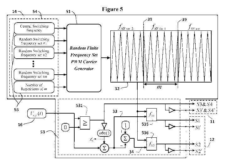
power converters.
Summary
[0005] Applicant has discovered that generating switching signals with
variable frequencies for
driving the switches of the high-frequency switches of various multi-level
converters (MLCs) can
lead to an imbalance of the energy storing components of the MLC.
[0006] Applicant has discovered that, for non-limiting embodiments
comprising flying-capacitor-
1
CA 03238219 2024-05-13
WO 2023/092224
PCT/CA2022/051721
based MLCs, this can lead to an imbalance of the flying capacitor's voltage
and that additional steps
must be taken when generating such signals for the charging and discharging of
the flying capacitor
(FC) to be better balanced.
[0007] The applicant has developed a pulse width modulation method for
generating the
switching signals with variable frequencies for a converter's high-frequency
switches that can better
balance the energy storing components of the MLC. For example, this can result
in a balancing of the
flying capacitor's voltage to reduce its high-frequency voltage ripples for
flying-capacitor-based
converters or can result in a balancing of the current of the leg inductors of
a 3L parallel converters.
[0008] The switching signal generator can be used to generate a
switching signal that induces half
.. a pulse for one of the charging/discharging states before the switching
frequency is varied and induces
half a pulse for the corresponding one of the discharging/charging states
(opposed state) after the
switching frequency is varied.
[0009] As experimentally demonstrated, this allows for significantly
suppressing the amplitude
of the high-frequency voltage ripples of the associated flying capacitor, thus
reducing the required
capacity and size of the FC, while still significantly reducing EMI and noise.
In some embodiments,
the switching signal generator can be digital and produce the described
switching signal via a
processor (microprocessor, DSP, FPGA, etc.) having a reference signal input.
[0010] In some embodiments, the switching signal regenerator is
completely or partially analog
or is completely or partially digital and is comprising a carrier signal, a
reference signal, and a
comparator for comparing these signals. In these cases, the half pulses of the
opposed
charging/discharging states at the switching frequency transition can be
achieved by shifting a carrier
signal by (2N-1)n radians (i.e., 180 ) when changing its switching frequency,
where N is a natural
number.
[0011] Applicants can implement this method to converters while
combining one or more pulse
width modulation methods. The converter can be and is not limited to a
rectifier, an inverter, a MLC
or a combination thereof In some embodiments, the MLC is a three-level or five-
level MLC. In some
embodiments, the MLC is used in a three-phase variable frequency motor drive.
In some
embodiments, a three-phase variable frequency motor drive comprising three
MLCs can have one
switching signal modulator for all of the switches of the converters. The
pulse width modulation
methods can be and are not limited to a random pulse-width modulation (RPWM),
random carrier-
frequency modulation, a novel random finite frequency set (RFFS) presented in
the description or a
combination thereof
2
CA 03238219 2024-05-13
WO 2023/092224
PCT/CA2022/051721
[0012] In some embodiments, the converter is equipped with fast power
switches operating at a
frequency of over about 50 kHz for reducing the value and size of the
capacitors, one or more pulse
width modulation methods are used to reduce noise and electromagnetic
interference, and the
developed method for modulating the carrier signal is implemented to reduce
both emanated
electromagnetic interference and the flying capacitor ripple induced by the
PWM.
[0013] In some embodiments, the switching signal regenerator is
generating signals for more than
the four switches connected to the flying capacitor.
[0014] In some embodiments, the switching signal generator is completely
digital and can access
a digital memory (non-transitory memory) storing one or more sequences of
switches pulses
respecting one or more of the PWM method comprising the described applicant's
contribution when
changing the switching frequency for generating one or more period of one or
more alternative AC
signals that can be repeated as needed.
[0015] Applicant proposes a first multi-level power converter comprising
a DC terminal, an AC
terminal, a flying capacitor, a pair of switches Si, Si' connected at one end
to the AC terminal and at
a second end to opposed terminals of the flying capacitor, a pair of switches
S2, S2' connected at one
end to opposed terminals of the flying capacitors and at a second end
connected directly or indirectly
to the DC terminal, where differential gating of the switches Si/Si' and the
switches S2/S2' causes
charging or discharging of the flying capacitor and common gating of the
switches Si/Si' and the
switches S2/S2' by-passes the flying capacitor, and a switching signal
generator for generating
switching signals for driving the switches Si, Si', S2, S2' having a reference
signal input and
comprising A) a variable frequency carrier signal generator for generating a
carrier signal with a
frequency that varies over time and a plurality of comparators connected to
the carrier signal and to
the reference signal for comparing the reference signal to the carrier signal
and having a comparison
output connected to respective gates of the switches Si, Si', S2, S2' or B) a
non-transitory memory
storing instructions and a processor operatively connected to respective gates
of the switches Si, Si',
S2, S2' for generating the switching signals for driving the switches at a
frequency that varies over
time. When the frequency that varies over time changes from one frequency to
another, a last switch
gate pulse at the one frequency is a half pulse for one of the switches Si/Si'
and the switches S2/S2'
and a first switch gate pulse of the other frequency is a half pulse for one
of the switches S2/S2' and
the switches Si/Si', respectively.
[0016] Applicant also proposes a second multi-level power converter
comprising a DC terminal,
an AC terminal, a first leg inductor connected to a first point of the AC
terminal, a second leg inductor
3
CA 03238219 2024-05-13
WO 2023/092224
PCT/CA2022/051721
connected to the first point of the AC terminal, a pair of switches Si, Si'
connected at one end to the
first leg inductor and at a second end to opposed terminals of the DC
terminal, a pair of switches S2,
S2' connected at one end to the second leg inductor and at a second end to
opposed terminals of the
DC terminal, where a differential gating of the switches Si/Si' and switches
S2/S2' causes
differential increasing and decreasing of energy stored in the first leg
inductor and the second leg
inductor, respectively, and common gating of the switches Si/Si' and the
switches S2/S2' causes
common increasing and decreasing of energy stored in the first leg inductor
and the second leg
inductor, respectively, and a switching signal generator for generating
switching signals for driving
the switches Si, Si', S2, S2' having a reference signal input and comprising
A) a variable frequency
carrier signal generator for generating a carrier signal with a frequency that
varies over time and a
plurality of comparators connected to the carrier signal and to the reference
signal for comparing the
reference signal to the carrier signal and having a comparison output
connected to respective gates of
the switches Si, Si', S2, S2' or B) a non-transitory memory storing
instructions and a processor
operatively connected to respective gates of the switches Si, Si', S2, S2' for
generating the switching
signals for driving the switches at a frequency that varies over time. When
the frequency that varies
over time changes from one frequency to another, a last switch gate pulse at
the one frequency is a
half pulse for one of the switches Si/Si' and the switches S2/S2' and a first
switch gate pulse of the
other frequency is a half pulse for one of the switches S2/S2' and the
switches Si/Si', respectively.
[0017] In some embodiments of the proposed multi-level power converters,
the switching signal
generator for generating switching signals for driving the switches Si, Si',
S2, S2' comprises A) a
variable frequency carrier signal generator for generating a carrier signal
with a frequency that varies
over time and a plurality of comparators connected to the carrier signal and
to the reference signal for
comparing the reference signal to the carrier signal and having a comparison
output connected to
respective gates of the switches Si, Si', S2, S2.
[0018] In some embodiments of the proposed multi-level power converters,
the switching signal
generator for generating switching signals for driving the switches Si, Si',
S2, S2' comprises B) a
non-transitory memory storing instructions and a processor operatively
connected to respective gates
of the switches Si, Si', S2, S2' for generating the switching signals for
driving the switches at a
frequency that varies over time.
[0019] In some embodiments of the proposed multi-level power converters,
the switches Si, Si',
S2, S2' are wide-bandgap fast power switches operating at a frequency of over
about 50 kHz.
[0020] In some embodiments of the proposed multi-level power converters,
where the frequency
4
CA 03238219 2024-05-13
WO 2023/092224
PCT/CA2022/051721
that varies over time comprises a discrete frequency set centered around a
central switching frequency
varied following a finite sequence, where the finite sequence is randomly
generated and periodically
repeated, where the frequency that varies over time is varied after generating
a number of pulses.
[0021] Some embodiments of the proposed multi-level power converters
further comprise
additional switches directly connected or indirectly connected to one of the
pair of switches and
directly connected or indirectly connected to the DC terminal or the AC
terminal, where the switching
signal generator is further generating switching signals for driving the
additional switches.
[0022] In some embodiments of the proposed multi-level power converters,
the switching signal
generator can further use any pulse modulation method in order to reduce
electromagnetic
interference, spread the harmonic cluster of switching frequency, cancel odd
multiples of switching
frequency, reduce harmonic cluster frequency spikes or a combination thereof.
[0023] Some embodiments of the first multi-level power converter further
comprise two
capacitors, where the second end of the pair of switches S2, S2' is connected
to a first end of the two
capacitors and is connected to the DC terminal, where the two capacitors are
connected at a second
end to neutral and together.
[0024] Some embodiments of the first multi-level power converter further
comprise a second
point of said AC terminal connected to the first ends of two capacitors whose
opposed second ends
are connected to opposed polarities of said DC terminal.
[0025] In some embodiments, an embodiment of the proposed multi-level
power converters is
used in a five-level active neutral point clamped converter configuration,
which further comprises two
high-voltage capacitors and additional switches, where a first pair S3, S3' of
the additional switches
is connected at a first end to the second end of a first one of the pair of
switches S2, S2', a second pair
S4, S4' of the additional switches is connected at a first end to the second
end of a second one of the
pair of switches S2, S2', a second end of a first one of the first pair S3,
S3' of the additional switches
is connected to a first end of a first one of the two high-voltage capacitors,
where the first end of the
first one of the two high-voltage capacitors is further connected to the DC
terminal, a second end of
a first one of the first pair S4, S4' of the additional switches is connected
to a first end of a second
one of the two high-voltage capacitors, where the first end of the second one
of the two high-voltage
capacitors is further connected to the DC terminal, and a second end of a
second one of the first pair
S3, S3' of the additional switches and a second end of a second one of the
first pair S4, S4' of the
additional switches are connected together, to second ends of the two high-
voltage capacitors, and to
neutral.
5
CA 03238219 2024-05-13
WO 2023/092224
PCT/CA2022/051721
[0026] Some embodiments of the proposed multi-level power converters can
be directly or
indirectly connected to at least one additional converter having at least one
switch, where the
switching signal generator generates switching signals for driving both the
switches of the multi-level
converter and the at least the one switch of the additional converter.
[0027] In some embodiments of the proposed five-level active neutral point
clamped converter is
a power rectifier for converting an alternative current to a direct current,
where the AC terminal is an
AC power input of the power rectifier and the DC terminal is a DC power output
of the power rectifier.
[0028] In some embodiments of the proposed five-level active neutral
point clamped converter is
a power inverter for converting a direct current to an alternative current,
where the DC terminal is a
DC power input of the power inverter and the AC terminal is the AC power
output of the power
inverter.
[0029] Applicant also proposes a bidirectional back-to-back converter
comprising an embodiment
of a proposed five-level active neutral point clamped power inverter, an
embodiment of a
corresponding five-level active neutral point clamped power rectifier, where
the AC power input of
the power rectifier is an AC power input of the bidirectional back-to-back
converter, where the AC
power output of the power inverter is an AC power output of the bidirectional
back-to-back converter,
where a negative DC current of the DC power output of the power rectifier is
connected to a negative
DC current of the DC power input of the power inverter, where a positive DC
current of the DC power
output of the power rectifier is connected to a positive DC current of the DC
power input of the power
inverter, where the neutral of the power rectifier is connected to the neutral
of the power inverter, and
where the power rectifier and the power inverter share of the two high-voltage
capacitors.
[0030] Applicant also proposes a three-phase variable frequency motor
drive comprising three of
a same embodiment of the proposed five-level active neutral point clamped
power inverter, where a
negative DC current of each one of the DC power input of the power inverters
are connected in
parallel, where a positive DC current of each one of the DC power input of the
power inverters are
connected in parallel, where the neutral of each one of the power inverters
are connected in parallel,
where the three of the power inverters share a common the two high-voltage
capacitors and share a
common the DC power input, and where the AC power output of each one of the
power inverters are
alternative currents phase-shifted by 120 degrees from the AC power output of
each other ones of the
power inverters.
[0031] Applicant also proposes a three-phase variable frequency motor
drive comprising three of
a same embodiment of the proposed bidirectional back-to-back converter, where
each one of the
6
CA 03238219 2024-05-13
WO 2023/092224
PCT/CA2022/051721
negative DC current of the three of the bidirectional back-to-back converters
are connected in parallel,
where each one of the positive DC current of the three of the bidirectional
back-to-back converters
are connected in parallel and where each one of the neutral of the three of
the bidirectional back-to-
back converters are connected in parallel, where the three of the
bidirectional back-to-back converters
share commons the two high-voltage capacitors, and where the power AC power
output of each one
of the three of the bidirectional back-to-back converters are alternative
currents phase-shifted by 120
degrees from the AC power output of each other ones of the three of the
bidirectional back-to-back
converters.
[0032] In some embodiments of the proposed three-phase variable
frequency motor drive, the
switches of the three-phase variable frequency motor drive are driven by a
common switching signal
generator.
[0033] Applicant further proposes a modulation method for power
conversion using a multi-level
power converter having at least one energy balancing component, which
includes: generating
switching signals for driving power switches of a multi-level power converter
connected to the at least
one energy balancing component at a frequency that varies over time to reduce
electromagnetic
interference of the multi-level converter, where, when the frequency that
varies over time changes
from one frequency to another frequency, a last switch gate pulse at the one
frequency is a half pulse
for at least one of the power switches and a first switch gate pulse of the
other frequency is a half
pulse for at least one other one of the power switches respectively, to
balance stored electric energy
of the at least one energy balancing component.
[0034] In some embodiments of the proposed method, the frequency that
varies over time is
repeated a fixed number of times, that is at least two times before being
changed to the other
frequency.
[0035] In some embodiments of the proposed method, the frequency that
varies over time changes
from the one frequency to the other frequency to perform random pulse width
modulation. In some
of these embodiments, the frequency that varies over time, the one frequency
and the other frequency
are selected from a discrete frequency set centered around a central switching
frequency. In some of
these embodiments, changing the one frequency to the other frequency is
following a finite sequence
that is randomly generated and periodically repeated.
[0036] In some embodiments of the proposed method, the switching signals is
generated by
comparing a reference signal to a triangular periodic signal having a
frequency of the frequency that
varies over time, where the last switch gate pulse and first switch gate pulse
are generated by phase
7
CA 03238219 2024-05-13
WO 2023/092224
PCT/CA2022/051721
shifting the triangular periodic signal by (2N-1)n radians (i.e., 1800, half a
period), or, in other words,
flipping around the horizontal axis (upside-down) when changing the frequency
that varies over time.
[0037] In some embodiments of the proposed method, the at least one
energy balancing
component is at least one flying capacitor, where the balancing of the stored
electric energy reduces
high-frequency voltage ripples of a voltage of the flying capacitor.
[0038] In some embodiments of the proposed method, the at least one
energy balancing
component is at least a pair of leg inductors, where each one of the pair of
leg inductors are connected
to a different pair of switches and where the balancing of the stored electric
energy reduces the
amplitude of current variations in the leg inductors.
Brief Description of the Drawings
[0039] The invention will be better understood by way of the following
detailed description of
embodiments of the invention with reference to the appended drawings, in
which:
[0040] Figure 1 is a schematic illustration of a five-level active
neutral point clamped (5L-ANPC)
converter, where its switches are controlled with the signal of the switching
signal generator.
[0041] Figure 2 is a table of switching states of the 5L-ANPC converter
presenting the associated
output voltages and the states for charging/discharging the various
capacitors.
[0042] Figure 3A illustrates switching signals for a high-frequency cell
of a MLC generated by
comparing reference signals to a carrier signal (m=3).
[0043] Figure 3B illustrates switching signals for a high-frequency cell
of a MLC generated by
comparing a novel carrier signal (m=3) to reference signals.
[0044] Figure 4A shows the flying capacitor voltage of a 5L-ANPC when
employing a carrier
signal (n=4, m=5, fs.,=110 kHz and step=10k Hz) RFFS-PWM schemes without
reduction of the FC
high-frequency ripples.
[0045] Figure 4B shows the flying capacitor voltage of a 5L-ANPC when
employing the same set
of RFFS-PWM schemes but using a proposed novel carrier signal (n=4, m=5,
fsw=110 kHz and
step=10 kHz) to reduce the FC high-frequency ripples.
[0046] Figure 5 illustrates the schematic diagram of a switching signal
generator for generating a
single-carrier logic equation-based switching signals that can respect the
random finite frequency set
PWM (RFFS-PWM) method for the 5L-ANPC converter.
[0047] Figure 6A shows a block diagram of a digital embodiment of part of
the comparator of the
switching signal generator.
[0048] Figure 6B shows a block diagram of a digital embodiment of the
carrier signal generator
8
CA 03238219 2024-05-13
WO 2023/092224
PCT/CA2022/051721
and another part of the comparator of the switching signal generator.
[0049] Figure 7A shows the harmonic spectrum of the output of the 5L-
ANPC converter by
applying the constant switching frequency single-carrier PWM method with the
switching frequency
off = 105 kHz.
[0050] Figure 7B presents the harmonic spectrum of the output of the 5L-
ANPC converter by
applying the conventional random PWM method with the switching frequency
around fsõ = 105 kHz.
[0051] Figure 8A presents the emanated EMI of the 5L-ANPC by applying
the proposed method
with the central switching frequency of f = 110 kHz, finite frequency sets of
n=4 with a step of 5
kHz and a number of repetitions of m=5.
[0052] Figure 8B presents emanated EMI of the 5L-ANPC by applying the
proposed method with
the central switching frequency of fs, = 110 kHz, a finite frequency set of
n=4 with a step of 10 kHz
and a number of repetitions of m=5.
[0053] Figure 8C presents emanated EMI of the 5L-ANPC by applying the
proposed method with
the central switching frequency of fs, = 110 kHz, a finite frequency set of
n=4 with a step of 20 kHz
and a number of repetitions of m=5.
[0054] Figure 8D presents emanated EMI of the 5L-ANPC by applying the
proposed method with
the central switching frequency of fs, = 100 kHz, a finite frequency set of
n=4 with a step of 15 kHz
and a number of repetitions of m=5.
[0055] Figure 9A shows a schematic illustration of a three-level flying
capacitor converter (3L-
FC) in a power inverter configuration, where its switches are controlled with
the signal of the
switching signal generator.
[0056] Figure 9B shows a schematic illustration of a three-level flying
capacitor converter (3L-
FC) in a power rectifier configuration, where its switches are controlled with
the signal of the
switching signal generator.
[0057] Figure 10 shows a schematic illustration of three 5L-ANPC inverters
in a three-phase
variable frequency motor drive configuration, where its switches are
controlled with the signal of the
switching signal generator.
[0058] Figure 11 shows a schematic illustration of three 5L-ANPC
rectifiers in a three-phase
active-front-end (AFE) rectifier configuration, where its switches are
controlled with the signal of the
switching signal generator.
[0059] Figure 12 shows a schematic illustration of six 5L-ANPC
converters in a three-phase
bidirectional back-to-back converter configuration, where its switches are
controlled with the signal
9
CA 03238219 2024-05-13
WO 2023/092224
PCT/CA2022/051721
of the switching signal generator.
[0060] Figure 13 shows a schematic illustration of a three-level (3L)
parallel converter with leg
inductors, where the energy balancing component of the circuitry is two leg
inductors instead of a
flying capacitor and where the switches are controlled with the signal of the
switching signal
generator.
Detailed Description
[0061] As fast switches, such as silicon carbide (SiC) or gallium
nitride (GaN) switches are
becoming more affordable, more and more power electronics apparatuses are now
using fast switches
in order to improve efficiency and reduce switching losses. However, replacing
standard switches
with these faster SiC and GaN switches cause significantly higher
electromagnetic interference (EMI).
To prevent further requiring an enlarged and redesigned EMI filter, techniques
of random pulse-width
modulation (PWM) have been developed to spread the harmonic cluster of
switching frequency
to adjacent frequencies, thus reducing the emanated EMI. However, the use of
such PWM methods,
such as the random PWM (RPWM) for example, can lead to an unbalance of the
stored electric energy
of the energy storing components of the converters. The energy storing
components of the converters
can be used to balance the energy across some of the switches, which are
therefore referred to as an
energy balancing component. The imbalance of stored electric energy in the
energy balancing
component can lead to an imbalance of the voltage of the flying capacitor in
flying capacitor-based
converters and can lead to non-equal current distribution between the leg
inductors in the parallel
converters with leg inductors.
[0062] For example, in the case where the energy balancing components is
a flying capacitor,
such PWM methods increases both the high and low-frequency voltage ripple
(LFVR) of the flying
capacitor (FC) of the multilevel converter (MLC). These greater voltage
ripples are not normally dealt
with and the MLC therefore requires the use of a higher value FC which can
increase the size, weight
and cost of the converter in addition to reducing efficiency.
[0063] The applicant has developed a pulse width modulation method for
generating the
switching signals with variable frequencies for a converter's high-frequency
switches that can better
balance some energy balancing components of the MLC. For example, this can
result in a balancing
of the flying capacitor's voltage to reduce its high-frequency voltage ripples
for flying-capacitor-
based converters or can result in a balancing of the current of the inductors
of a three-level (3L)
parallel converters.
[0064] Applicant has found a method for generating switching signals to
balance the charging and
CA 03238219 2024-05-13
WO 2023/092224
PCT/CA2022/051721
discharging of the FC as to reduce its voltage ripples and is thus able to
create more efficient MLCs,
while still significantly reducing EMI and noise.
[0065] For better understanding, let us consider an exemplary embodiment
of converter having a
flying capacitor (FC) as an energy storing component as illustrated in Figure
1. Figure 1 presents a
schematic illustration of an embodiment of a hybrid flying capacitor based
MLC, more specifically a
five-level active neutral point clamped (5L-ANPC) converter provided with a DC
power supply 15
of voltage E. In other embodiments, MLCs are alternative derived hybrid
configurations of the 5L-
ANPC 10 comprising a DC-link capacitor regulated to E/2, a high-frequency FC
cell 12 (S1, SI, S2
and S2') and a low-frequency voltage doubler cell 11 (S3, S, 54 and S4'). The
various switches of
the MLC are controlled with the switching signals delivered by the switching
signal generator 14 in
response to a reference voltage (Võf) 16, which can be implemented digitally,
analogically or with a
combination thereof. In some embodiments, only some switches are fast power
switches, while in
some other embodiments all of the switches are fast power switches. In this
embodiment, the high-
frequency cell is comprising a FC 13 regulated to E/4 and a first set of four
fast power switches (SiC
.. and/or GaN switches). This 5L-ANPC converter is used to generate five
output voltage levels Vout as
a function of the eight possible switching states S. as presented in the table
of figure 2. In this
embodiment, utilizing the possible redundant switching states allows to
regulate the FC without using
any voltage sensor or closed-loop voltage regulator and to generate five
various output voltages
(Vout): 0, +E/4 or +E/2 voltage levels. Figure 2 also indicates the charging
CD and discharge (1,)
states of the DC capacitors (LE) and of the energy balancing element, which in
this embodiment
is the flying capacitor (AEcdc), for each of the switching state and output
voltages. The frequency of
switching in the range of 10 kHz to 30 kHz in a MLC can be considered to be
efficient for silicon-
based slower switches, while the frequency of switching can be increased to be
above 50 kHz to over
100 kHz for fast power switches. Such higher frequency can reduce the size of
the flying capacitors
and/or inductors in the MLC and improve efficiency. The effect of faster
switches and higher
frequency is to increase switching noise, namely EMI noise in the MLC output.
[0066] In order to reduce the FC's voltage ripples, the imbalance of the
charging and discharging
state must be minimized at all times, which can be achieved by balancing the
width of the active time
for the switching states of the high-frequency cell 12 responsible for
charging and discharging of the
FC. As illustrated in Figure 2, the embodiment's FC 13 is solicited when only
one of the fast switches
Si or S2 is active (differential gating), meaning that the charge on the FC is
kept constant when both
of them are in the same state. However, the task of balancing the pulse width
of the high-frequency
11
CA 03238219 2024-05-13
WO 2023/092224
PCT/CA2022/051721
cell switches can often become a much-complicated task when employing complex
PWM methods
within MLCs, especially when employing random PWM methods.
[0067] Random modulation schemes for generating PWM switching signals of
switches of the
converter can involve comparing reference signals to carrier signals with
randomized switching
frequency or randomized pulse positions. This can be used for common random
modulation schemes
such as random pulse-position modulation (RPPM) and/or random pulse-width
modulation (RPWM)
and/or random carrier-frequency modulation with a fixed duty cycle (RCFMFD),
etc.
[0068] To better understand the relation of the carrier signal (Crr) and
VRef for generating
switching signals, refer to Figure 5 illustrating an embodiment a switching
signal generator 14, where
a carrier signal 32 generated by a carrier signal generator 51 is compared
with the reference signal 16
through a logic equation-based comparator 53 in order to generate the
switching signals for the
switches of both the low-frequency cell 11 and the high-frequency cell 12. It
will be appreciated that
carrier signal generator 51 can be configured to utilize a set of
stored/integrated values and functions
54 that can include various functions 55, which may be central switching
frequencies, random
switching frequencies and numbers of repetitions (m). In the non-limiting
embodiment of Figure 5,
the comparing blocs Li 535 and fs2 536 are comparing modified reference
signals (VRef ,1 = Z,' +
VRef) 33, where Z, = 1 when VRef <0 or else is zero, and (VRef,2 = 1 ¨ VRef,i)
34 with the Crr 32
to generate the switching signals for the switches S1 and S2, respectively.
Where the comparing
process of the comparing blocs fs1 535 and fs2 536 of this embodiment can
respect the following
logic equations (1) and (2), respectively.
S = / 1, VRef,i Crr
1
¨1, VRef ,1 < Crr (1)
S = 1, VRef,2 Crr
2
¨1, VRef ,2 > Crr (2)
[0069] Figure 3A illustrates exemplary switching signals 30' and 31' for
the high-frequency cell
of the 5L-ANPC generated by comparing Crr 32' to the reference signals VRef ,1
33 and VRef,2 34 for
the switches S1 and S2, respectively. In the embodiment of Figure 3A, the
switching signals are a
result of a proposed pseudorandom binary sequence generator, for generating a
finite quantity of
random values used to select the following/adjacent frequency (f,+i) out of a
finite switching
frequency variation band which reduces the switching losses, where the
switching frequencies
are repeated three times (m=3) before changing to fsi+1. The full transition
pulses 36 (around the
change between two different fs, 39), having a width larger than the preceding
pulse and smaller than
12
CA 03238219 2024-05-13
WO 2023/092224
PCT/CA2022/051721
the following one, cause an imbalance of the charging/discharging of the FC
over time when repeated
and applied only to some of the switches (to S2 in this example). In this
setup, the switching signal Si
does not have any transition pulse inducing an imbalance with S2 when charging
and discharging the
FC.
[0070] In fact, this imbalance is responsible for inducing the above-
mentioned low-frequency
voltage ripple (LFVR) 40 of the FC 13 seen on the experimental curve of the FC
voltage as of function
of time presented in Figure 4A. The high-frequency voltage ripples of the FC
identified as 41, are
caused by the logic equation of the comparator and are of reasonably low
intensity.
[0071]
Identifying the specific source of the LFVR is part of the solution
allowing to develop a
new method for generating the carrier signal. Applicant has found that the
LFVR can be suppressed
up to about 60% with this new method that manages the pulses of the high-
frequency cell's switches
around each of the switching frequency change 39 (fsw, to
The switching signal generator can
be used to generate a switching signal that induces half a pulse for one of
the charging/discharging
states before the switching frequency is varied and induces half a pulse for
the corresponding one of
.. the discharging/charging states (opposed state) after the switching
frequency is varied.
[0072]
In the embodiments presented above and all embodiments comprising a
carrier signal, the
method can include phase shifting the following set of switching frequency
(fs+i) by (2N-1)n
radians (i.e., 180 , half a period), or, in other words, flipping around the
horizontal axis (upside-down)
the Crr each time the switching frequency is changed. This results in the
alternative and novel carrier
signal 32 illustrated in Figure 3B, which depicts exemplary switching signals
30 and 31 for the high-
frequency cell of the 5L-ANPC generated by comparing the novel Crr 32 to the
reference signals
VRef,1 33 and VRef,2 34 (the same reference signals as Figure 3A) for the
switches Si and S2,
respectively respecting the logic equations (1) and (2). This allows to
symmetrically balance the
charging and discharging of the flying capacitor by inducing half a switch
pulse in the charging or
discharging ,I, state (see Figure 2 for specific states of the presented
embodiment) before the switching
frequency change 39 and half a switch pulse in the opposite state (discharging
,I, or charging T,
respectively). In other words, this method equally imposes and distributes
half transition pulses (37
and 37') to the charging and discharging states.
[0073]
The resulting experimental curve of the FC voltage as of function of
time presented in
Figure 4B shows a reduction of about 15 volts (60%) of the LFVR 40 from the
conventional carrier
signal illustrated in Figure 4A (from about 25 volts to about 10 volts) when
using the novel carrier
signal.
13
CA 03238219 2024-05-13
WO 2023/092224
PCT/CA2022/051721
[0074] While the presented carrier signal 32 is illustrated as the
preferred embodiment of a
triangular wave, but one skilled in the art will appreciate that Crr 32 can
take the form of a left or
right sawtooth wave or any triangular shape in between. While not being
limited by the following,
this method is most useful when used in combination with frequency modulation
schemes for the
switching signals of the switches in most of the converters (rectifiers,
regulators, inverters, converters,
two-level converters, three-level converters, five-level converters, etc.)
comprising an energy storing
element (e.g., flying capacitor, leg inductor), acting as an energy balancing
component, connected
with at least some of the switches, since these frequency modulation schemes
can cause unbalanced
charging and discharging of the energy storing element of the converters.
[0075] In some of the preferred embodiments of the flying capacitor-based
converters, switches
can cause charging or discharging of the FC when differentially gated (half of
the switches are active
while their respective opposed corresponding switch is inactive). An uneven
switching of the switches
that can result from the frequency modulation schemes currently used, in the
state of the art, for the
switching signals of the switches can therefore induce an imbalance of the
charging/discharging of
the stored electrical energy (e.g., the voltage of the flying capacitor). The
proposed PWM method can
reduce this imbalance of the stored electrical energy in the energy
storing/balancing elements of
converters.
[0076] Exemplary MLC switching signal generator
[0077] The embodiment of a 5L-ANPC illustrated in Figure 1, can have a
switching signal
generator illustrated in Figure 5 as a schematic diagram of a proposed random
finite frequency set
(RFFS) PWM for the 5L-ANPC converter. As shown in Figure 5, the proposed RFFS-
PWM can be
divided to the two following main submodules: the RFFS-PWM carrier generator
51 for generating
the proposed symmetrical charge/symmetrical discharge carrier signal of the
RFFS-PWM method 32
with the variable inputs 54; and a logic equation-based comparator cell 53, to
compare the carrier
signal 32 with the reference signal 16.
[0078] As someone skilled in the art would know, both of these
submodules can be analog or
digitally implemented with one or more processors (microprocessor, digital
signal processor, field-
programmable gate array (FPGA) and/or others). They can be separately
programmed or integrated
together. In some embodiments, a carrier signal generator is integrated into
an FPGA (with defined
switching frequency variation update rates and a list of all fsw) for
generating a RFFS-PWM Crr is
working with at least one comparator programmed in a microprocessor having
this Crr and a
reference signal as inputs. In some embodiments, the FPGA is programmed so
that the fsõ is selected
14
CA 03238219 2024-05-13
WO 2023/092224
PCT/CA2022/051721
by following a pseudorandom binary sequence that signals a triangular signal
generator module to
generates a period with the selected frequency (by controlling the triangular
signal generator module's
internal counter or clock) repeated m times and that also signals the
triangular signal generator module
to phase shift the next period by (2N-1)n radians (i.e., 1800) when the
changing fsw. Figure 6A
.. presents the block diagram of a digital embodiment of the comparator of the
switching signal
generator for generating VRef,1 33, VRef,2 34 and switching signal for the LF
cell 11. Figure 6B shows
a block diagram of the same digital embodiment of the carrier signal generator
51 and another part of
the comparator for comparing Crr 32 to the modified reference signals VRef,1
33 and VRef,2 34 of
Figure 6A to generate the switching signals of the HF cell 12.
[0079] In some similar or analogue embodiments, the switching signals can
be partially or
completely generated via software by referring to a readable non-transitory
memory storing one or a
list of multiple (up to many gigabytes of data) predetermined sequences of
modulated pulse width
simulating the required level of randomness that can be adapted to a reference
signal and repeated as
many times as possible. For example, a switching signal predetermined to be a
pseudorandom
sequence (for reducing noise and losses and improving the efficiency of the
converter) for generating
at least one full AC period can be repeated as many times as needed.
[0080] In this embodiment, the RFFS-PWM carrier generator 51 submodule
generates n number
of switching frequency sets with symmetrical distribution around the central
switching frequency of
fsw. To attain symmetrical switching harmonic cluster distribution around the
central switching
frequency of fsw, n may be selected as an even number. The bandwidth of
switching frequency
variation (BT/1') between two adjacent switching frequencies of fSW#kand ¨ fcw
#k+i may be defined in
a way that maximum continuous switching frequency harmonic distribution can be
achieved. So, the
BVVsw can be defined by the equation (3), where k E [1; n - 1].
fsw#k+i-fsw#k , k = -n
2 2
[0081] BVVsw = (3)
k -n
fsw#k+i tsw#k 2
[0082] The BVVsw may be selected based on the desired band of the interest
defined by the relevant
standards. The random switching between the frequencies of the finite
switching frequency set
(around central switching frequency) is controlled by referring to and
employing a finite set of random
values generated with a pseudorandom binary sequence generator with a
bandwidth of switching
variation that can be BVVsw.
[0083] The number of repetitions 55 can be defined as the switching
frequency variation update
CA 03238219 2024-05-13
WO 2023/092224
PCT/CA2022/051721
rate (m). The switching pattern of the novel proposed carrier signal 32 is
presented in Figure 5. As
depicted, the switching frequency f can be updated to a next switching
frequency selected out of a
finite list of n numbers of I's, with a value selected from the pseudorandom
binary sequence. By
employing this technique in this embodiment of the proposed RFFS-PWM method,
the average value
of switching loss of the converter can be approximately equal to that value of
the standard constant
switching frequency PWM techniques. Regarding other introduced RPWM
techniques, it is worth
mentioning that without utilizing this technique, the switching loss of the
converter can be increased,
and its value can be higher than that value by employing the constant
switching frequency PWM
techniques. Hence, by applying the number of repetitions (m) 55 to the
submodule 51, the efficiency
of the converter may be increased in comparison to other RPWM methods.
[0084] In order to achieve sensor-less voltage balancing of the FC in
the 5L-ANPC and 3L-FC
MLCs, the charge/discharge period of the FC should be balanced in each
switching period. Balancing
the charge/discharge period is difficult to fulfill in random pulse position
RPWM methods due to the
fast variation of pulse position or duty cycle. Similarly, as previously
described and illustrated in
Figure 3A, due to the fast variation of the switching frequency fs, in
dithering technique (based on
changing the switching frequency without manipulating the pulse position in
RPWM techniques), it
is difficult to balance charge/discharge period in each switching period. This
leads to an increased
value of required FC and increased voltage ripple of the FC. In order to solve
this issue, the applicant
uses the novel symmetrical charge/symmetrical discharge method to generate a
carrier signal 32
similar to the one illustrated in Figure 3B. The charge/discharge period of
the FC is balanced in each
switching period by employing this proposed PWM method. As illustrated, the FC
charge/discharge
period is balanced in each m = 3 repetitions of switching periods as an
auxiliary FC voltage
balancing. Therefore, there are two sensor-less FC voltage balancing
algorithms in this embodiment
of the proposed RFFS-PWM method. The first one can be utilized in the logic
equation-based single-
carrier PWM which balances the FC voltage in each switching period and the
second one can be the
(2N-1)n radians phase shift of the carrier signal when changing switching
frequency which balances
the FC voltage in each m repetition.
[0085] The schematic diagram of the hybrid single-carrier sensor-less
PWM method for the 5L-
ANPC MLC with capacitors and a self-voltage balancing comparator cell 53 is
also presented in figure
5. It is comprising one PWM carrier signal (Crr) and two logic equations to
generate PWM signals
for the 5L-ANPC inverter. In this embodiment of the introduced hybrid single-
carrier PWM method;
S3, S3f , 54 and 541 are considered as one low-frequency (LF) cell 11 whereas
Si, SI, S2 and S21 are
16
CA 03238219 2024-05-13
WO 2023/092224
PCT/CA2022/051721
considered as one high-frequency (HF) cell 12, as illustrated in figure 1. In
the embodiment of Figure
5, a simple zero-crossing comparator 531 is used with a reference signal Võf
(16) to generate the
symmetric and equal switching signals (S3. S, S4 and S4') for the low-
frequency cell 11 in one
fundamental period, wherein S3 = S4 = 1 when Võf 0 and S3 = S4 = 0 when Võf <
0. In this
embodiment, the modified reference voltage 33 VRef,1 is compared to the Crr by
the logic functions
535 and 536 in order to provide the PWM switching signals (S1, SI, S2 and S2')
for the high-speed
switches of the high-frequency cell 12.
[0086] Figure 7A shows the harmonic spectrum (the light gray is the
common-mode noise and
the darker gray is the differential noise) of the output of an embodiment of
the 5L-ANPC converter
by applying the constant switching frequency single-carrier PWM method with
the switching
frequency of f = 105 kHz. In this embodiment, the multiples of the switching
frequency are
canceled out at the output of the 5L-ANPC and the first switching harmonic
cluster frequency is
shifted to twice of the switching frequency, but the needle type harmonic
cluster spikes are still present
at even multiples of fs, and the maximum peak value of emanated EMI 70 is
around 130 dB[tV.
Figure 7B presents the harmonic spectrum (the light gray is the common-mode
noise and the darker
gray is the differential noise) of the output of a similar embodiment of the
5L-ANPC converter using
the conventional RPWM method with the same switching frequency of f = 105 kHz,
where the
peak value of emanated EMI 71 is around 80 dB[tV and where the odd multiples
of the switching
frequency are not yet canceled out since the first switching harmonic cluster
72 is at fs, (105 kHz)
instead of double its value (210 kHz), hence the values of the required output
passive filters are
significantly increased.
[0087] Figures 8A, 8B, 8C and 8D present the emanated EMI (the light
gray is the common-mode
noise and the darker gray is the differential noise) of an embodiment of the
5L-ANPC by applying
the proposed method with the central switching frequency of fs, = 110 kHz, a
number of repetitions
of m=5 and a finite frequency set of n=4 with alternative step values. The
finite frequency steps value
is of 5 kHz (100 kHz, 105 kHz, 110 kHz, 115 kHz and 120 kHz) in Figure 8A, 10
kHz (90 kHz, 100
kHz, 110 kHz, 120 kHz and 130 kHz) in Figure 8B, 20 kHz (70 kHz, 90 kHz, 110
kHz, 130 kHz and
150 kHz) in Figure 8C and 15 kHz with f = 100 kHz (70 kHz, 85 kHz, 100 kHz,
115 kHz and 130
kHz) in Figure 8D. The experiment results for the alternative finite frequency
steps, the first and odd
multiples of the switching harmonic clusters are canceled out and the peak
value of EMI (all
associated with the differential mode noise) is around 80 dB[tV 80, 79.9 dB[tV
81, 98.5 dB[tV 82 and
97.5 dB[tV 83, respectively. The pulse width modulation methods can be and are
not limited to
17
CA 03238219 2024-05-13
WO 2023/092224
PCT/CA2022/051721
random pulse width modulation, random carrier-frequency modulation, random
finite frequency set
or a combination thereof.
[0088] This proposed method can be implemented to converters while
combining one or more
pulse width modulation methods. The converter can be and is not limited to a
rectifier, an inverter, a
MLC or a combination thereof. In some embodiments, the MLC is a five-level
MLC, a three-level
converter, a three-level inverter as illustrated in Figure 9A, a three-level
rectifier as illustrated in figure
9B, etc. It will be appreciated that a three-level converter (e.g., 3L-FC or
3L parallel converter) or a
five-level converter, including the described 5L-ANPC, can also be used as a
power inverter (DC in,
AC out), a power rectifier (AC in, DC out) and/or a combination thereof, such
as a five-level or three-
level hybrid variable-frequency AC power converter by connecting the output of
a five-level or three-
level rectifier to the input of a five-level or three-level inverter. In some
embodiments, the MLC is
used as a three-phase variable frequency motor drive. In some embodiments, a
three-phase variable
frequency motor drive comprising three MLCs can have one switching signal
modulator for all of the
switches of the converters, where the reference signal 16 is used to generate
tree phase-shifted
reference signals (120 phase shift between each of these reference signals)
be compared to the same
carrier signal 32 to drive the three-phase variable frequency motor.
[0089] Figure 10 shows an embodiment of such a three-phase variable
frequency motor drive that
utilizes three switch cell 101 (pair of LF 11 and HF 12 cells) of five-level
inverters connected in
parallel at their positive DC current 102, neutral 103 or ground and negative
DC current 104
connections to generate three AC power outputs 106 phase-shifted by 120
degrees used to drive a
three-phase motor 109. In this embodiment, the three switch cells 101 are
sharing a common DC
terminal circuitry 105, which can comprise a DC power input (VDc) and a pair
of high-voltage
capacitors (Ci and C2). This embodiment can also comprise a motor side filter
107 before the motor
inputs and a field orientated control 108 for controlling the three-phase
variable frequency motor drive
output in order to adjust the switching signal generated by the switching
signal generator and generate
proper output voltage and frequency to control the motor.
[0090] It will be appreciated that the switching signal generator can be
used to drive the switches
of MLC in a three-phase active-front-end rectifier configuration. Figure 11
shows one embodiment
of such a three-phase rectifier that utilizes three switch cell 101 of five-
level inverters connected in
parallel at their positive current 102, neutral 103 and negative current 104
connections to generate a
single DC power output 106. In this embodiment, while each of the three switch
cells 101 have an
AC power input (Va , V b or 10, they share a common DC terminal circuitry 105,
which can comprise
18
CA 03238219 2024-05-13
WO 2023/092224
PCT/CA2022/051721
a pair of high-voltage capacitors (Ci and C2) and a single DC power output
(VDc) 106. Some
embodiments can also comprise an input filter 111 before the switch cells; a
current controller 112
for controlling the AC input currents and a voltage regulator 113 to adjust
the switching signal
generated by the switching signal generator and regulate the output DC voltage
to its desired value.
[0091] Figure 12 shows one embodiment of a three-phase bidirectional back-
to-back converter
comprising the MLC of Figure 11 connected the MLC of Figure 10 at their high-
frequency capacitors
connections (negative DC current 104 to negative DC current, neutral 103 to
neutral and positive DC
current 102 to positive DC current). In this configuration, the inputs are
three AC voltages Va, Vb and
vc (one for each input switching cells) and the outputs are three AC outputs
106 phase-shifted by 120
degrees used to drive a three-phase motor 109. This embodiment can also
comprise an input filter 111
before the power rectifier switch cells (101, 101' and 101"); a current
controller 112 for controlling
the AC input currents, a voltage regulator 113 for regulating the DC link
voltage, a motor side filter
107 before the motor inputs and/or a field orientated control for adjusting
the AC outputs. The
described embodiments can comprise a switching signal generator for each one
of the switching cells,
a single switching signal generator for all of the cells or any configuration
in between.
[0092] While the MLC presented in this description was focused on 5L-
ANPC, 3L parallel
converter and 3L-FC, it will be appreciated that the MLC can be any
alternative configuration that
comprises a flying capacitor, including; flying capacitor multicell (FCM)
converters, stack multicell
(SM) converters, N-level ANPCs, full-bridge modular multilevel converters (FB-
MMC), half-bridge
modular multilevel converters (HB-MMC), quadrupled neutral point clamped (Q-
NPC) converters,
quadrupled hybrid neutral point clamped (Q-EINPC) converters, etc.
[0093] While most of the present disclosure focuses on embodiments
comprising flying
capacitors as the energy storing circuitry component of the circuitry
presented herein (5L-ANPC, 3L-
FC, etc.), it will be appreciated by someone skilled in the art that,
alternative converters comprising a
variety of alternative energy storing circuitry components used to balance the
energy across the
circuitry, herein referred to as an energy balancing component (e.g., flying
capacitor, inductors, leg
inductors), can utilize the proposed switching method. In fact, the proposed
single-carrier RFFS-
PWM method can serve to reduce energy variation (e.g., voltage ripples in
flying capacitors, current
ripples in leg inductors) across the alternative energy balancing circuitry
components some of these
alternative converters.
[0094] While the embodiments of converters presented herein can comprise
a flying capacitor
(FC) in which the FC voltage is regulated to its desired value by applying the
proposed RFFS-PWM
19
CA 03238219 2024-05-13
WO 2023/092224
PCT/CA2022/051721
method without utilizing any additional voltage sensor and closed-loop voltage
controller, the
proposed sensor-less single-carrier RFFS-PWM method can also be applied to
alternative three-level
converters (alternative or dual circuits) of the 3L-FCM converter. In an
embodiment, the dual three-
level FCM converter can be a three-level parallel converter as schematized
diagram in Figure 13.
[0095] It will be appreciated by someone skilled in the art that electrical
dualities, in electrical
terms, are associated into pairs called duals. For example, a dual of a
relationship is formed by
interchanging voltage and current in an expression.
[0096]
The embodiment of a 3L parallel converter as schematized in Figure 13
can comprise
circuitry components similar to the ones comprised in the embodiments of a 3L-
FCM illustrated in
Figure 9A and 9B. A 3L parallel can comprise a high-frequency double leg
inductor cell 18, which
can include a pair of inductors 19 (e.g., leg inductors) connected on one side
(at one end) to an AC
terminal (VAcj), to pairs of switches (e.g., Si/Si' and S2/S2') each connected
at one end the another
opposed end of one of the pair of a different of the leg inductors (e.g., leg
inductor 1 and leg inductor
2, respectively). The 3L parallel can further comprise a DC terminal having
each of its terminals (e,g,
VDC+ and VDc-) connected to another opposed end of the pairs of switches
(S1/S1' and S2/S2') and to
a first end of one of a pair of capacitors (e.g., Cdc+ and Cdc-,
respectively), where both of the other ends
of the pair of capacitors (Cdc+ and Cdc-) are connected to an AC terminal
(VAc;2). Note that a 3L parallel
may not have any flying capacitor as an energy storing component since the
energy balancing
component can be the two inductors (e.g., leg inductors). The two pairs of
switches can be
controlled/driven by an embodiment of the switching signal generators 14.
[0097]
Applying the proposed single-carrier RFFS-PWM method to dual three-level
converters
which include the 3L-FCM and the 3L-parallel converters comprising dual energy
balancing
components including flying capacitor in the 3L-FCM converter and leg
inductors in the3L parallel
converter, dual operation of the three-level converters can be achieved. For
example, 3L parallel
converters can have dualities to 3L-FCM converter when employing the proposed
RFFS-PWM, which
can include the following:
¨ Both the voltage value of the flying capacitor 13 of a the 3L-FCM
converter and the currents
of the two inductors 19 of a 3L parallel converter can be regulated/balanced.
¨ As for a 3L-FCM converter, odd multiples of the switching harmonic
clusters can also be
canceled out in the 3L parallel converter which can also lead to significant
improvement,
similarly to the 3L-FCM converter, of the switching harmonic spectrum of the
3L parallel
converter.
CA 03238219 2024-05-13
WO 2023/092224
PCT/CA2022/051721
¨ As for a 3L-FCM converter, the proposed symmetrical charge/discharge method
that may
be utilized in the proposed RFFS-PWM method can also lead to a balancing of
the current of
the leg inductors 19 of a 3L parallel converter.
Accordingly, it will be appreciated that the proposed RFFS-PWM method as
presented herein
can also be applied to the 3L parallel converter in the same way in the 3L-FCM
converter.
21