Note : Les descriptions sont présentées dans la langue officielle dans laquelle elles ont été soumises.
1~6653S
Specification
Title of the Invention
Multiplexer
Background of the Invention
The present invention relates to a multiplexer
and, more particularly, to a multiplexer for inserting a
frame synchronization code, a service code, or the like in
a digital data signal train.
In a sending end in digital multiplex
communications, a multiplexer having a function for
multiplexing digital data signals and various code signals
in time slots in response to a clock signal having a
predetermined frequency plays an important role. Fig. l
shows a conventional multiplexer. This multiplexer
basically comprises a l/M frequency divider 1, a l/N
frequency divider 2, and a selector 3.
Fig. 2 is a timing chart of signals generated in
the multiplexer shown in Fig. 1. Referring to Figs. 1 and
2, the frequency divider 1 receives a clock signal S10 for
determining a length of one time slot and generates a
signal S11 every M time slots. The signal Sll is input to
the frequency divider 2 and to an input terminal S0 of the
selector 3.
The frequency divider 2 generates N signals S22-1
to S22-N having different phases on the basis of the output
signal 511 of the frequency divider 1. The signals S22-1
- l - 'J~
~ 266S35
to S22-N are input to the input terminals Sl to SN of the
selector 3, respectively. It should be noted that M
usually represents 16 to 30 and N represents 4 to 8. For
illustrative convenience, however, M = 4 is given.
The selector 3 has (N + l) data input terminals
DO to DN, (N ~ 1) control signal input terminals SO to SN,
and one data output terminal 0. The data input terminal Di
is paired with the corresponding control signal input
terminal Si, where i is O to N. If the nth control signal
input terminal Sn is set at logic "1", the signal input to
the paired data input terminal Dn appears at the output
terminal 0.
Referring to Fig. l, a digital data signal train
S13-0 is input to the data input terminal DO of the
selector 3. The output signal Sll of the frequency divider
1 is input to the control signal input terminal SO. N
insertion code signals S13-1 to S13-N are respectively
input to the data input terminals Dl to DN of the selector
3. The output signals S22-1 to S22-N from the frequency
divider 2 are respectively input to the control signal
input terminals Sl to SN.
In the digital data signal string S13-0, each
digital data signal using (M - 1) time slots (three in this
embodiment) and each gap G of one time slot alternately
appear.
The signal Sll is set at logic "1" for three time
slots in which digital data is present in the digital data
1266535
signal train 13-0 and is set at logic "O" for one time slot
in which digital data is not present therein.
~ he content of each of the N insertion code
signals Sl3-1 to S13-N is kept unchanged for a time
interval between the start and end output signals S22-1 and
S22-N output ~rom the frequency divider 2, as shown in
Fig. 2. Therefore, the frequency of the insertlon code
signal is set to be 1/(N x M) of the digital data signal
train Sl3-0.
The selector 3 outputs the digital data signal
train S13-0 for a period in which the output signal S11
from the frequency divider 1 is kept at logic "1".
However, the selector 3 outputs the insertion code signals
S13-1 to S13-N in time slots respectively corresponding to
the phases of the output signals S22-l to S22-N from the
frequency divider 2. As shown in Fig. 2, the insertion
code signals (iO5, ill, il2, il3, il4, il5, i21,...) are
properly inserted in the digital data signal train S13-0,
thereby preparing a multiplexed signal S16.
An arrangement of the selector 3 used in Fig. 1
is shown in Fig. 3. The selector 3 includes (N ~ 1)
2-input AND circuits 51-0 to 51-N and a plurality of
multi-input OR gates 52, both of which constitute a
multiple stage. A maximum operating frequency of the
selector 3 is determined by the operating speeds of the
respective logic circuits and propagation delay times
between the respective stages. The selector 3 having the
1;~66535
above arrangement is not suitable for high-speed digital
signal processing, because it has to process signals of
different speeds, i.e., the high-speed digital data signal
train S13-0 and the low-speed insertion code signals whose
frequency is l/(N x M), e.g., a maximum of 1/240, of the
digital data signal. In other words, the operating
frequency of the multiplexer depends on the number of
insertion code signals, and therefore, the high-speed
multiplexing cannot be achieved. Also, when the total
propagation delay time of the circuit is so long that a
predetermined operating frequency cannot be obtained, the
selector 3 must be opened at a predetermined position
thereof, and a circuit element for controlling the
operation timings must be inserted in the opened position.
This results in that the size of the selector 3
is increased in proportion to the number of insertion
codes, and power consumption is undesirably increased.
Even if a relatively low frequency is set so as
to allow use of MOS (metal oxide semiconductor) devices
which consume less power and these devices are used, the
propagation delay time of the circuit is further increased
to greatly decrease the digital~signal processing
frequency.
Summary of the Invention
It is an object of the present invention to
eliminate the conventional drawbacks described above, and
1266535
has as its object to provide a simple, high-speed
multiplexer.
A multiplexer according to the present invention
comprises: a first frequency divider for receiving a clock
signal which determines a multiplexing time slot and
outputting a first signal every M time slots, M being an
integer and equal to or greater than 2; a second frequency
divider for receiving the first signal from said first
frequency divider and generating N second signals having
different phases, N being an integer and equal to or
greater than 2; first selector means for converting N
insertion codes into one code signal train on the basis of
the second signals; and second selector means for receiving
a digital data signal train having an alternate repetition
of a digital data signal using (M - 1) continuous time
slots and a gap of one time slot and for inserting the
insertion codes of the code signal train into the gap of
one time slot on the basis of the first signal.
Brief Description of the Drawings
Fig. 1 is a block diagram showing a conventional
multiplexer;
Fig. 2 is a timing chart of signals generated in
the multiplexer shown in Fig. l;
Fig. 3 is a circuit diagram showing an
arrangement of a selector shown in Fig. 1;
Fig. 4 is a block diagram of a multiplexer
according to an embodiment of the present invention; and
1266535
Fig. 5 is a timing chart of signals generated in
the multiplexer shown in Fig. 4.
Detailed Description of the Preferred Embodiment
A preferred embodiment of the present invention
will be described with reference to the accompanying
drawings. Fig. 4 is a block diagram of a multiplexer
according to an embodiment of the present invention, and
Fig. 5 is a timing chart of signals generated in the
multiplexer shown in Fig. 4.
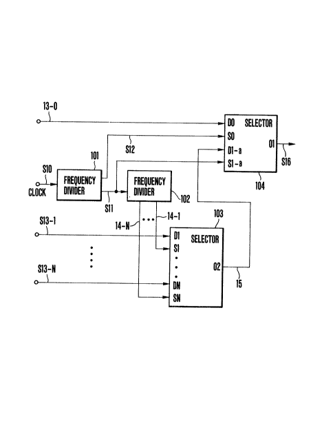
Referring to Fig. 4, a frequency divider 101
receives a clock signal SlO for determining a time slot and
generates a signal Sll and its inverted signal S12 every M
(e.g., M = 4) time slots.
A frequency divider 102 receives the output
signal S11 from the frequency divider 101 and generates
signals S14-1 to S14-N having N te.g., N = 5) phases and
each having a pulse width of M time slots.
A selector 104 has a pair of data and control
signal input terminals D0 and S0, another pair of data and
control signal input terminals D1-a and S1-a, and an output
terminal 01. When signal inputs to the control signal
input terminals S0 and S1-a are set at logic "1", signal
inputs to the data input terminals D0 and D1-a appear at
the output terminal 01, respectively.
A selector 103 has N pairs of data and control
signal input terminals D1 and S1, D2 and S2,... DN and SN,
and an output terminal 02. When a signal of logic "1" is
~z66~i3~
input to the control signal input terminal Sj, when j is 1
to N. A signal input to the data input terminal Dj paired
with the terminal Sj appears at the output terminal 02.
The arrangement of the selector 103 is substantially the
same as that of the conventional selector shown in Fig. 3
and comprises a multi-stage coupling of N 2-input AND
circuits and a multi-input OR circuit.
The output signal Sll of the frequency divider
101 is supplied to the input terminal of the frequency
divider 102 and the control signal input terminal Sl-a of
the selector 104. The output signal S12 of the frequency
divider 101 is supplied to the control signal input
terminal SO of the selector 104.
The output signals S14-1 to S14-N of the
frequency divider 102 are respectively supplied to the
control signal input terminals S1 to SN of the selector
103. The output terminal 02 of the selector 103 is
connected to the data input terminal D1 of the selector
104.
A digital data signal train S13-0 consisting of
digital data D using (M - 1) continuous time slots and a
gap of one time slot, as previously described, is supplied
to the data input terminal DO of the selector 104 at a
timing shown in Fig. 5.
Insertion code signals S13-1 to S13-N having a
frequency of 1/(N x M) of the digital data signal train
~26653S
S13-0 are respectively supplied to the data input terminals
Dl to DN of the selector 103.
The insertion code signals S13-1 to S13-N are
converted into one code signal train S15 in accordance with
the output signals S14-1 to S14-N of the frequency divider
102. The code signal train S15 is supplied from the output
terminal 02 to the data input terminal Dl of the selector
104. Therefore, the same output signal S16 as in the
conventional multiplexer appears at the output terminal Ol
of the selector 104.
According to the present invention as has
described above, the selector 103 having a multistage
coupling of a large number of logic circuit elements can be
operated at l/(N x M) of the frequency of the digital data
signal train S13-0. Therefore, the allowable margin of the
circuit propagation delay time can be increased. In
addition, since the selector 104 only comprises a pair of
2-input AND circuits and an OR circuit, the number of
circuit elements can be reduced, and the operating
frequency can be increased.
The operating frequency of the multiplexer
according to the present invention does not depend on the
number of insertion codes but on the propagation delay time
of the a pair of 2-input terminal selector 104, thereby
achieving high-speed multiplexing.
In the multiplexer according to the present
invention as described above, the N insertion codes
~2~;653S
requiring only low-speed processing are time-serially
converted into a code si~nal train by the first selector.
Subsequently, the digital data signal train and the code
signal train are time-serially multiplexed by the second
selector. Therefore, the number of circuit elements of the
second selector is small. In other words, a circuit having
a short propagation delay time can be arranged, and thus
the operating frequency of the circuit can be increased.
Furthermore, since the circuit size of a portion
subjected to high-speed processing can be reduced, power
consumption can be reduced, and MOS devices can be used,
thus providing many advantages.