Sélection de la langue

Search

Sommaire du brevet 1271819 

Énoncé de désistement de responsabilité concernant l'information provenant de tiers

Une partie des informations de ce site Web a été fournie par des sources externes. Le gouvernement du Canada n'assume aucune responsabilité concernant la précision, l'actualité ou la fiabilité des informations fournies par les sources externes. Les utilisateurs qui désirent employer cette information devraient consulter directement la source des informations. Le contenu fourni par les sources externes n'est pas assujetti aux exigences sur les langues officielles, la protection des renseignements personnels et l'accessibilité.

Disponibilité de l'Abrégé et des Revendications

L'apparition de différences dans le texte et l'image des Revendications et de l'Abrégé dépend du moment auquel le document est publié. Les textes des Revendications et de l'Abrégé sont affichés :

  • lorsque la demande peut être examinée par le public;
  • lorsque le brevet est émis (délivrance).
(12) Brevet: (11) CA 1271819
(21) Numéro de la demande: 536842
(54) Titre français: BLINDAGE ELECTRIQUE
(54) Titre anglais: ELECTRICALLY SHIELDING
Statut: Réputé périmé
Données bibliographiques
(52) Classification canadienne des brevets (CCB):
  • 339/11
  • 356/11
(51) Classification internationale des brevets (CIB):
  • H05K 1/02 (2006.01)
  • H05K 9/00 (2006.01)
  • H01R 13/658 (2011.01)
  • H01R 12/16 (2006.01)
  • H01R 13/658 (2006.01)
(72) Inventeurs :
  • KERN, WALTER PHELPS (Etats-Unis d'Amérique)
(73) Titulaires :
  • TERADYNE, INC. (Etats-Unis d'Amérique)
(71) Demandeurs :
(74) Agent: SMART & BIGGAR LLP
(74) Co-agent:
(45) Délivré: 1990-07-17
(22) Date de dépôt: 1987-05-11
Licence disponible: S.O.
(25) Langue des documents déposés: Anglais

Traité de coopération en matière de brevets (PCT): Non

(30) Données de priorité de la demande:
Numéro de la demande Pays / territoire Date
893,221 Etats-Unis d'Amérique 1986-08-05

Abrégés

Abrégé anglais


Abstract
A shielding device, as for spring pins, is provided
by providing a base having shielding holes, grounding holes,
and a trough connecting them with an interconnected covering,
providing within the shielding holes insulators with element
holes therethrough.

Revendications

Note : Les revendications sont présentées dans la langue officielle dans laquelle elles ont été soumises.


THE EMBODIMENTS OF THE INVENTION IN WHICH AN EXCLUSIVE
PROPERTY OR PRIVILEGE IS CLAIMED ARE DEFINED AS FOLLOWS:

1. An electrically shielding device which comprises:
a base,
said base being formed of insulating material and having
therein
a shielding hole and
a shield connecting hole,
said shielding hole having positioned therein
a metallic shield therearound,
an insulator within said shield, and
an element hole in said insulator, and
said shield connecting hole having positioned therein an
electrically conductive layer, said layer being in electrical
communication with said shield.


2. The device of claim 1 in which said shield and said
layer are coatings.


3. The device of claim 2 in which one continuous coating
provides said coatings and said electrical communication.


4. The device of claim 3 in which said continuous coating
is of plated metal.


5. The device of claim 4 in which said metal is electroless
nickel.

6. The device of claim 2 in which said base and said
insulator are of plastic.


7. The device of claim 6 in which said insulator is glass-
loaded polyphenylene sulfide and said insulator is of castable
polytetrafluoroethylene, and said metal is electroless nickel.

8. The device of claim 3 in which a trough connecting said
shielding hole and said shield connection hole is covered by said
continuous coating.

9. The method of fabricating a shielding device which
comprises forming an insulating base, providing therein a first
hole and a second hole, coating said base over said holes with a
layer of conductive material, placing in said first hole an
insulating material with a third hole therethrough, and
electrically interconnecting the coatings in said first and second
holes.


10. The method of claim 9 in which said base is coated
overall, and top and bottom surfaces are thereafter cut to
electrically segregate said first and second holes.


11. The method of claim 10 in which a channel connecting
said first hole and said second hole is coated therewith to
provide said electrically interconnecting.


Description

Note : Les descriptions sont présentées dans la langue officielle dans laquelle elles ont été soumises.


1;~71~1~

ELECTRICAL~Y SHIELDING
Field of the Invention
This invention relates to electrically shielding, and
more particularly, in preferred embodlments, to the coaxlal
~hielding of sprlng pins.
Backaround of the Invention
The desirablllty of shleldlng elements of electrlcal
clrcults, ln approprlate lnstances, ls well known. Coaxially
shlelded ~prlng plns for u6e ln connectlon wlth prlnted circuit
boards ("PCB~") are known.
Su-marY of the Invention
I have discovered that coaxlal 6hieldlng may be
provlded, reliably, at low expense and consi6tently wlth hlgh
~hlelded element denslty, by provldlng an lnsulator base having
shlelded element and groundlng element mountlng holes, the lnner
wall of a grounding element mountlng hole belng ln conductlve
electrlcal communlcatlon with a shield around a shlelded element
mountlng hole and spaced therefrom by lnsulatlng materlal.
Accordlng to a broad aspect of the lnventlon there ls
0 provlded an electrlcally shleldlng devlce which comprises~
a base,
said base belng formed of in~ulating materlal and havlng
thereln
a shleldJng hole and
a shleld connectlng hole,
. sald ~hleldlng hole havlng posltioned thereln
a metalllc shleld therearound,


~ 1


an insulator wlthin ~aid shield, and
an element hole in said insulator, and
said shield connecting hole having positioned therein an
electrically conductive layer, said layer being in electrical
communication with said shield.
According to another broad aspect of the invention there
i8 provided the method of fabricating a æhielding device which
comprlses forming an lnsulatlng base, provlding thereln a flrst
hole and a second hole, coating said base over said holes with a
layer of conductlve materlal, placing in said first hole an
insulatlng material with a third hole therethrough, and
electrlcally interconnecting the coatlngs in said first and second
holes.
In preferred embodlments, the insulator base is a
unltary ~tructure molded from polyphenylene sulfide reinforced
with glass and containing a multlpllcity of spring pin mountlng
holes orlented ln pairs, one sprlng pln mountlng hole of each palr
belng spaced by a polytetrafluoroethylene lnsulatlng annulus from
an electroless nlckel ghleld around the annulus, the other sprlng
pin mountlng hole of each palr belng conductlvely connected to the
~hleld by a contlnuum of the electroless nlckel.
In another aspect of the inventlon, I have dlscovered
that such a coaxlal shleldlng devlce may be provlded by formlng an
ln~ulatlng base containlng a palr of holes therethrough, platlng
the base wlth metal, removlng the metal from top and bottom
surfaces of the base, and formlng ln one of the holes an annulus
of lnsulatlng materlal. In a preferred embodlment a bllnd slot ls


~d

~.27181~

provided between the two holes before plating.
Preferred E~bodiment
Following is a description of preferred embodiments of
the device and method of the invention.
Drawing~
There is shown in:
Flgure 1 an lsometric view of a broken-away portion
showing one shleld portion of the preferred embodiment of the
device.
Flgure 2 a correspondlng lsometric view illustrating an
earlier stage ln the preferred embodlment of the method.
Flgure 3 a dlagrammatlc plan vlew of a broken away
portlon of the devlce.
Flgure 4 a plan vlew on a smaller scale of an
arrangement of sald devices.
Figure 5 a sectional view taken at 5-5 of Figure 3.
Figure 6 a correspondlng sectlonal vlew showlng a second
devlce cooperatlng wlth a flrst in order to ~ecure therebetween a
sprlng pln.
8tructure
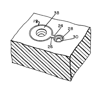
There i~ shown ln Flgure 3 an enlarged plan vlew, and ln
Flgure 1 an lsometrlc vlew, of a portlon of one of the devlce~,
indlcated generally at 10, of the lnventlon. In use, elght of
these devlce~ 10, the lnner and outer walls 12 and 14 of whlch are
coaxlally arcuate (O.D. 10 lnches) are abutted to form an
arrangement annular ln horlzontal cro~s-sectlon, as shown in plan
vlew ln Flgure 4.


~ 3

71~

Referring to Figures 2 and 5, each devlce 10 has a base
16 formed by lnjection molding of glass-filled (40%) polyphenylene
sulfide (sold by Phillips Chemlcal Company under the trademark
RYTON R-4). ~xtending through base 16 are cylindrically annular
layers 18, 20 of dull (for better adhesion) electroless nlckel.
The layer extends ln a continuum along the floor 22 and sides 24,
26 of bllnd slot 27 and therefrom in portlons 28, 30 of
counterbore 32 and cylindrlcal portion 34 wlthin hole 36. Annular
ca~t tetrafluoroethylene lnsulator 38 ca~tlng materlal ~sold by
DuPont under the trademark TEFZEL) iB wlthln electroless nlckel
layer 18, 20 and fill~ slot 27. Hole 40 wlth counterbores 42 is
provlded ln lnsulator 38.
As ~hown in Flgure 6, two unlt~ 10 are brought together
wlth sprlng plns indlcated generally at 43 held therebetween ln
one set of counterbores 32, 42 for each sprlng pln. (Counterbores
32, 42 are provided at each end of holes 36, 40 80 that the ring
44 made up of unlts 10 may be used with either surface up, to
permlt moldlng a slngle base 16 even though two configurations of
base 16 are needed, for example alternatlng around the annulus,
one belng a mlrror lmage of the other. The rlng 44 may be held
together and down on a PCB (not shown) by screws (not ~hown), and
permlts easlly releasably connectlon therethrough wlth another PCB
(not shown).
OPeration
Current passlng through sprlng plns 43 ln lnsulator 38
18 electrically shlelded by electrodless nickel completely
therearound, the latter belng electrlcally connected wlth the


~ 4

~ 7181~
69204-130
ad~acent ground spring pin through a continuing layer of
electroless nickel. Hole 36, in which the ground spring pin is
located, thus is a shield connecting hole, in that the layer of
nickel electrically connects the pin in it to the shield of the
adjacent shielded pln.
Hethod
The device is made by first molding the base 16, giving
it an overall thickness about 0.020 inches greater than ultimately
wanted. The entire piece is then given a coating of dull
electroless nickel, which extends over top, bottom and throughout
the large and snall hole, counterbore, and slot as ~hown ln the
uncoated piece ~hown ln Figure 2. About 0.010 inch thlckness ls
then removed ~rom top and bottom, removlng wlth lt the nlckel
coating thereover. Bushing 38 is then cast.
Other E-bodi~ents
Other embodlments wlll occur to those skllled ln the
art.


4a


,
.~,~, , , , ;

Dessin représentatif
Une figure unique qui représente un dessin illustrant l'invention.
États administratifs

Pour une meilleure compréhension de l'état de la demande ou brevet qui figure sur cette page, la rubrique Mise en garde , et les descriptions de Brevet , États administratifs , Taxes périodiques et Historique des paiements devraient être consultées.

États administratifs

Titre Date
Date de délivrance prévu 1990-07-17
(22) Dépôt 1987-05-11
(45) Délivré 1990-07-17
Réputé périmé 2007-07-17
Correction de l'état expiré 2012-12-05

Historique d'abandonnement

Il n'y a pas d'historique d'abandonnement

Historique des paiements

Type de taxes Anniversaire Échéance Montant payé Date payée
Le dépôt d'une demande de brevet 0,00 $ 1987-05-11
Enregistrement de documents 0,00 $ 1987-07-24
Taxe de maintien en état - brevet - ancienne loi 2 1992-07-17 100,00 $ 1992-06-08
Taxe de maintien en état - brevet - ancienne loi 3 1993-07-19 100,00 $ 1993-06-09
Taxe de maintien en état - brevet - ancienne loi 4 1994-07-18 100,00 $ 1994-06-17
Taxe de maintien en état - brevet - ancienne loi 5 1995-07-17 150,00 $ 1995-06-14
Taxe de maintien en état - brevet - ancienne loi 6 1996-07-17 150,00 $ 1996-06-18
Taxe de maintien en état - brevet - ancienne loi 7 1997-07-17 150,00 $ 1997-06-25
Taxe de maintien en état - brevet - ancienne loi 8 1998-07-17 150,00 $ 1998-06-25
Taxe de maintien en état - brevet - ancienne loi 9 1999-07-19 150,00 $ 1999-07-02
Taxe de maintien en état - brevet - ancienne loi 10 2000-07-17 200,00 $ 2000-07-04
Taxe de maintien en état - brevet - ancienne loi 11 2001-07-17 200,00 $ 2001-07-03
Taxe de maintien en état - brevet - ancienne loi 12 2002-07-17 200,00 $ 2002-07-03
Taxe de maintien en état - brevet - ancienne loi 13 2003-07-17 200,00 $ 2003-07-03
Taxe de maintien en état - brevet - ancienne loi 14 2004-07-19 250,00 $ 2004-07-02
Taxe de maintien en état - brevet - ancienne loi 15 2005-07-18 450,00 $ 2005-07-04
Titulaires au dossier

Les titulaires actuels et antérieures au dossier sont affichés en ordre alphabétique.

Titulaires actuels au dossier
TERADYNE, INC.
Titulaires antérieures au dossier
KERN, WALTER PHELPS
Les propriétaires antérieurs qui ne figurent pas dans la liste des « Propriétaires au dossier » apparaîtront dans d'autres documents au dossier.
Documents

Pour visionner les fichiers sélectionnés, entrer le code reCAPTCHA :


Pour visualiser une image, cliquer sur un lien dans la colonne description du document. Pour télécharger l'image (les images), cliquer l'une ou plusieurs cases à cocher dans la première colonne et ensuite cliquer sur le bouton "Télécharger sélection en format PDF (archive Zip)" ou le bouton "Télécharger sélection (en un fichier PDF fusionné)".

Liste des documents de brevet publiés et non publiés sur la BDBC .

Si vous avez des difficultés à accéder au contenu, veuillez communiquer avec le Centre de services à la clientèle au 1-866-997-1936, ou envoyer un courriel au Centre de service à la clientèle de l'OPIC.


Description du
Document 
Date
(yyyy-mm-dd) 
Nombre de pages   Taille de l'image (Ko) 
Dessins représentatifs 2001-09-18 1 10
Dessins 1993-10-07 1 46
Revendications 1993-10-07 3 52
Abrégé 1993-10-07 1 9
Page couverture 1993-10-07 1 12
Description 1993-10-07 5 149
Taxes 1996-06-18 1 32
Taxes 1995-06-14 1 44
Taxes 1994-06-17 1 48
Taxes 1993-06-09 1 23
Taxes 1992-06-08 1 29