Note : Les descriptions sont présentées dans la langue officielle dans laquelle elles ont été soumises.
--1--
CLOCK REiCOYERIN(:; DE~ICE
BACXGROUND OF THE INVENTION
The present invention relates to a clock reco~ering device
and, more particularly, to a device for accurately recovering a
clock from received da~a which has a different dutY ratio of
5 logical ONEs and lo~ical ZEROs.
For the recovery of a clock from received data, it has been
customary to detect a transition of the incoming data and, if the
recovered clock is low level (or high level) at the instant of
detection of a transition, retard lor advance) the phase of the
10 recovered clock deciding that the phase is advance~d (or
retarded). In this manner, a prior art clock recoverin~ device
corrects the phase of a recovered clock timed to transitions of
received data. However, a problem with such a device is that
when the duty ratio of ONEs and ZEROs of received data is
15 different, even if the phase of a recovered cloclc is greatlY
deviated, the Phase is decided as being advanced and retarded
alternately everY time a transition is detected. This indefinitelY
prevents a clock from being correctly recovered.
Sl)MMARY C)F THE IN~ENTION
It is, therefore, an object of the present invention to provide
a cloclc recovering device capable of accurately recovering a
clock from received data despite a difference of duty ratio.
It is another object of the present invention to provide a
generally improved clock recovering device.
A clock recovering device of the present invention comprises
an edge detector for producin~ a pulse when received data
changes, a first counter for counting a high-speed clock which is
an integral multiple times higher than a transmission rate of the
~L~7~ 3
received data, and reset by the pulse output by the edge
detector, a logic unit for processing an O~ltpUt of the first
counter, a second counter for receiving an output of the logic
unit and reset bY the pulse for counting the hi~h-speed clock, a
phase comparator for deciding a phase of recovered clock timed
to a carry which is output by the second counter, alld a variable
frequency divider controlled in frequencY division number by an
output of the phase comparator for producing the recoYered
clock from the high-speed clo-~k.
In accordance with the present invention, a deYice for
recovering a cloc~ from received data which has a different duty
ratio determines the optimum timing of a recovered clock based
on the pulse width of received data. A clock is accurately
recovered so long as the duty ratio of received data is not
greater than + 5 0 ~ .
BRIEF DESCRIPTIOM OF THE DRAWINGS
Figs. 1 and 2 are timing charts demonstrating the operation
of a prior art clock recovering device;
Fig. 3 is a block diagram showing a cloclc recovering deYice
embodying the present invention;
Fig. 4 is a timing chart repreSentatiYe of the operation of
the clock recovering device in accordance with the present
inventiort,
S Fig. S is a block diagram showing another embodiment of
the present invention; and
Fig. 6 is a chart showing data stored in a ROM (Read Only
Memory) which is included in the device of Fig. 5.
DESCRIPTION OF THE PREFERRED EMBODIMENTS
To better understand the present invention, the operation of
a prior art clock recovering device will be outlined with reference
to Figs. 1 and 2. As shown in Fig. 1, it is a common practic0
to correct the phase of recovered clock by detectinæ a transition
of receiYed data and, if the recovered clock is low level at the
8,.~
--3--
instant of detection of a transition, retarding the phase deciding
that the phase is advanced and, if it is high level, advancing the
phase deciding that the phase is retarded. As previously stated,
such a prior art implementation indefinitely fails to correctly
5 recover a clock if the duty ratio is not greater than -~ 50 %,
because, as shown in Fig. 2, the phase is decided as being
advanced and retarded alternately timed to the transitions of
received data even if the phase of the recovered clock is greatly
deviated.
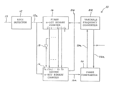
Referring to Fi8. 3, a clock recovering device embodYing the
present invention and which is free from the drawback discussed
above is shown. The clock recovering device, generally 10,
comprises an edge detector 12 to which received data 13 is
applied, a first n-bit binary counter 14 which is supplied with an
15 output l 2 a of the edge detector 12, a second n-bit binary
counter 16 which is also supplied with the outPut 12a of the edge
detector 12, an inverter 18 connected to the first n-bit binary
counter 14, a phase comparator 2 0 to which an output 16 a of
the second n-bit binary counter 16 is coupled, and a variable
20 frequency divider 22 which receives an output 20a of the phase
comparator 20 and, in turn, feeds its output 22a to the phase
comparator 20.
The operation of the clocls recovering device 10 will be
described with reference to Fig. 4. In the figure, "n" is assumed
25 tobe3.
Assume that the width of a logical high or a logical low pulse
of the received data 13 is Tp, the period of the received data 13
is To, and the deviation of duty is greater than -50 % and
smaller than ~50 %. Then, if the data length is 1, the timing of
30 recovered cloclc is 0. 5Tp before because Tp is equal to or
greater than 0. 5To and smaller than 1. 5To; if the ~ata length is
2, the timing of recovered clock is 0. 5 (Tp - To) before because
Tp is equal to or greater than l. 5To and smaller than 2. 5 To;
if the data length is 3, the timing of recoYered clock is 0. 5 (Tp -
35 2To) before because Tp is e~ual to or ~reater than 2. 5To and
33
smaller than 3. 5To; and if the data length is m, the timing of
recovered clock is 0. 5 [Tp - (m - 1) To ] before because Tp is
equal to or greater than (m - 0. 5) To and smaller than (m +
O. 5)To
Upon transition of the re~eived data 13 from high to or low
or vice versa, the edge detector 12 produces a pulse 12 a. The
first n-bit binary counter 14 counts a high-speed clock 24 which
is 2 n times hi~he~ than the transmission rate of received data.
The counter 14 is reset by each pulse 12a to reach the same
count at every period T, so that the count I immediately before
resetting is produced by:
. = Tp--(m--1) To 7
(when (m - 0. 5~To ~ Tp ( mTO)
( n ~) To _Tp--(m--1) To~
(when mTO ( Tp ( (m + 0. 5)To)
Since a relation 2n-t ~ I ~ 2n - 1 holds under a condition of
(m - 0. 5) To ( Tp ( mTO and a relation 0 ~ I ( 2n-' holds under
a condition of mTO ~ Tp ( (m + 0. 5) To, the timing of
recovered clock is expressed as:
0.5~T?--(~--l)To)-- (0.5~)
2D.
(where I ) 2n-t~
=-- ( 0.5 ~ + 2 ) ,
(where I ( 2n-~)
As shown in Fig. 3, the "n-l" to "1" bit outputs of the first
35 n-bit binary counter 14 are connected to, respectively~ the "n-2"
~L~7~
to "0" bit inputs of the second n-bit binary counter 16. Further,
the "n- 1 " bit output of the first counter 14 is conllected to the
"n-1" bit input of the secolld counter 16 by way of the inverter
18. Assuming that the value read in response to the pulse 12a is
5 K, there holds an equation:
0~5 ~ ~p~ 1 ) To
(let the error of - be neglected)
2n~1
Hence, what is stored in the second n-bit binary counter 16 is a
time interval between the optimum timing of recovered clock and
a transition of received data.
Since the second n-bit binarY counter 16 continuouslY counts
1 i the high-speed clocls 24, its carry 1 6a coincides in timing with
the optimum timing of recovered clock. The carry 1 6a and the
recovered clock 22a are fed to the phase comparator 20 which
then decides the phase of the recovered clock 22a and produces a
phase correct signal 2 0 a. In resPOnse, the variable frequency
20 divider 22 changes the frequencY division number to thereby
correct the phase of the recovered clock 22a.
Referrin~ to Fig. 5, another embodiment of the present
invention is shown. This embodiment is essentially the same in
construction as the embodiment of Fig. 3 except for the
25 provision of a first and a second N-bit counter 26 and 28 and a
ROM 30 which serves as a decoder. By the operation which will
be describeid, the clock recovering device of Fig. 5 recovers a
clock in the same manner as the device of Fig. 3, when N is X.
The ROM 30 computes L = 0. 5N + 0. 5M (where M ( 0. 5N) and
30 L = 0. 5M (where M ) 0. 5N) based on a count m of the first
N-bit counter 26.
Turnin~ back to Fig. 4, as the received data 13 chan~es
- from high to low or vice versa, the edge detector 12 produces a
pulse 12a. Counting the high-sPeed clock 24 which is N times
35 higher than the received data trartsmission rate, the first N-bit
counter ~6 is reset by each pulse 12a to reach the sarne count at
each period T. Hence, the count M immediatelY before resetting
is produced by:
T
5Tp ~ 1 ) To = M - --~
(when (m - 0. 5~To ( Tp ( mTO)
( N+ ~
N
(when mTO ( Tp ( (m + 0. 5) To )
Since M is the count of the N-bit counter, relations M ) 0. 5N and
~I ( O. 5N hold under conditions of (m - 0. 5) To ( Tp ( mTO and
15 mTO ( Tp (m + 0. 5)To, resPectively. Further, there holds an
equation:
Tp ~ 1 ) To--M o
N
~0 (where M ) 0. SN)
= (N+M) TQ
(where M ~ 0. 5N~
Therefore, the timing of reco-Yered clock is Produced by:
T
0.5~Tp~ 1) To~= O.5M- N
(where M ) 0. 5N)
--(0.5N~O.SM) N
(where M ~ 0. 5N)
The "0", "1", ..., "n - 1" bit outputs of the first N-bit
counter 2 6 are fed to, respectivelY, the "Ao", "A~ ", . . ., "An
bits of the :E~OM 30. The ROM 30 computes L = 0. 5M ~M )
Q. 5N) and L = 0. 5N + 0. 5M ~M ( 0. 5N) (data stored in the
5 ROM 30 when N is 8 are shown in Fig. 6~, the results appearing
on the ''OO'', "O,", ..., "n-l" bits. The second N bit counter
28, therefore, is loaded with a time interval between the
optimum timing of recovered clock and a transition of received
data.
Since the second N-bit counter 28, too, has a period of Tol
its carr~ 28a coincides in timing with the optimum timin~ of
recovered clock. Subsequently, as in the first embodiment, the
carry 28a and the recovered clock 22a are applied to the phase
comparator 20. In response, the Phase comparator 20 decides
the phase of the recovered clock 22a and, then, Produces a
phase correct signal 20a. The variable frequencY divider 22
chan~es the frequencY division number by usin~ the phase
correct signal ~Oa, thereby correcting the phase of the recovered
clock 22a.
2 0 In summary, it will be ssen that the present invention
provides a clock recovering device which accuratelY recovers a
clock if the duty ratio of received data is not greater than +50
%, because it determines the optimum timing of recovered clock
based OIl the pulse width of received data.
2 5 Various modifications will become possible for those skilled
in the art after receiving the teachings of the present disclosure
without departing from the scope thereof.