Note : Les descriptions sont présentées dans la langue officielle dans laquelle elles ont été soumises.
7~i~35
- 1 -
METHOl~ OF FABRICATINC~ MULTILAYF.R STRUCTURES
WITH NONPLANAR SUl~F~CES
Background of the Invention
One of the contenders for future semiconductor electronic packaging
schemes is the chip cavity multilayer board. The structure basically comprises
multiple layers of printed wiring board material with conductors on one or more
5 major surfaces of each layer. The layers are bonded together by an appropriateaclhesive. Included in the structure is a cavity where the semiconductor chip isbonded and electrically connected to pads on the various layers. This chip cavity
multilayer board can then be attached to a standard printed wiring board including
other components.
One of the problems associated with fabricating this structure involves
bonding together the various layers. If not properly controlled, the adhesive tends
to flow from between the layers of printed wiring board material into the cavity as
a result of the application of heat and pressure during bonding. This Iesults intight manufacturing tolerances, since too little flow of the adhesive can result in
15 lack of circuit encapsulation and voids between the layers.
Another problem associated with ~abricating this type of structure
involves the bending and deformation of wire bonding pads during the bonding
process. Deformed and distorted wire bonding pads are not suitable for automatedwire bonding assembly of the chip.
20 SummarY of the Invention
The invention is a method of fabricating a multilayer structure which
includes a nonplanar surface defined by said layers. A flowable adhesive is
provided between the layers for bonding the layers together~ A release material
and a conformal material are provided over the str~lcture including the cavity.
25 Heat and pressure are applied to the structure to cause the conformal and release
materials to fill the recesses in the nonplanar surface and thereby prevent the flow
of the adhesive into the recesses.
Brief ~escription of the Drawin~
These and other features of the invention aue delineated in detail in
30 the following description. In the drawings:
F~G. 1 is a perspective, cut-a~ay view of a typical multilayer structure
which may be fabricated in accordance with the invention, and
~ ;I''~`
.. . . .
' . . : ' : ' ' ' '
:
- . ., ~: ' ' ," ' ' ~
- ~ .
.
75~
FIGS. 2-3 are cross-sectional views of the multilayer str~lctwre of
FIG. 1 during different stages of fabrication in accordance with one embodiment
of the invention.
It will be appreciated that, for the sake of illustration, these figures are
5 not necessarily drawn to scale.
l~etailed Description
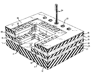
FIG. 1 illustrates a typical cavity multilayer board which can be
fabricated in accordance with the invention. The bottom substrate layer, 10, in
this example, is a mixture of bismaleimide, triazine and epoxy, and includes
10 conductive elements, e.g., 11 and 12, on both major surfaces. Also included on
the substrate is a conductive pad 13 for bonding a semiconductor chip thereto (not
shown). Multiple layers, 15 and 1~, are located over and properly registered with
the substrate, 10. These layers are typically the same type of printed wiring board
laminate material as the substrate and also include conductive members on both
15 major surfaces, e.g., 17 and 18, as well as via holes, e.g., 19, electrically connecting the conductors on opposite surfaces.
The multiple layers, 15 and 16, define a cavity, 20, for placement of
the chip. The cavity typically measures approximately .9 cm x 1.2 cm at its baseand 1.0 cm x 1.3 cm at the top with a height of .065 cm. Conductive pads, e.g.,
20 21 and 22, are included on the top surfaces o~ the two layers, 15 and 16, near the
edges defining the cavity so that electrical connections can be made to the chip by
wire bonding to the pads.
Plated through holes, e.g., 23, are provided through the entire structure
so that conductive pins, such as 24 may be inserted therein. These pins provide
25 the electrical connection to the next level of interconnection such as a printed
wiring board.
The multiple layers, 15 and 16, are typically bonded to the substrate
and to each other by an appropriate adhesive, 25 and 26, provided between the
substrate and first laye~ (15~ and between the first and second (16) layers. The30 adhesive is typically a no ~9OW or low flow, partially polymerized, material which
is preimpregnated with glass fabric ~known in the art as B-stage prepreg
adhesive). In this example, the adhesive was a bismaleimide-triazine-epoxy
mixture impregnated E-glass telectrical grade) fabric. Other standQrd adhesives
can be employed. Two or more adhesive layers are stacked and aligned in the
35 structure after appropriate CQVity cutouts are t`ormed in each layer. Next, heat and
,:
. .. : : . ,
, ' ': ' . ' :" : ',
31.~'75~3~
pressure are applied to form a permanent bond between the layers. The bonding
is typically done by increasin~ the temperature at a rate in the range o~
5C/minute -30C/minute to a maxirnum temperature in the ran~e 160 - 190C
which is held for a period of 30-90 minutes. The applied pressure is typically
5 .8 - 4.8 megapascals. This bonding causes the adhesive to i~ow and can, therefore,
result in adhesive flowing into the cavity (including the area over the bonding
pads 21).
FIG. 2 illustrates a portion of a multilayer structure d~lring one stage
of fabrication in accordance with an embodiment of the invention. It will be
10 appreciated that many packages such as shown in FIG. 1 are batch fabricated from
a multilayer board panel which is typically approximately 46 cm x 61 cm with
many cavities formed therein. FIGS. 2 and 3, therefore, show only the portion ofthe multilayer structure which will eventually result in a single package.
PIG. 2 illustrates the stage where the multiple layers, 15 and 16, have
15 been stacked over the substrate, 10, with the adhesive layers, 25 and 26, provided
therebetween, b~lt prior to the lamination operation which will produce final
bonding between the layers and substrate. Optionally, a template, 30, is provided
on top of the multilayer structule. (The template is shown in the figures as lifted
slightly above the multilayer structure for purposes of illustration.~ This template
20 is a thin sheet of material, in this case type 300 stainless steel with a thickness of
approximately .046 cm, which has openings therein corresponding in size and
position to the cavities formed in the multilayer structure. The purpose of the
template ;s to distribute the stresses during the bonding operation to minimize
bending of the edges of the layers 15 and 16 which include the bonding pads 21
25 and 22. Consequently, the template should be thin enough not to interfere with
the bonding process, but thick enough and with enough bending strength to
minimize bending of the layers at the cavity edges. A thickness of 250 ~ 750
microns is useful for this function. The template material should also have a
coefficient of thermal expansion similar to the multilayer structure. In addition to
30 stainless steel, a double-clad copper laminate approximately 350 microns thick
was suitable.
Provided over the multilayer structure and template is a combination
of a release film 31 and ~owable conformal material 32. In particular, the release
material, 31, which is in the form of a sheet, was placed on the template, 30, over
35 the entire area of the panel including the portion shown in FIG. 2. I'he conformal
.
~ ~ .
';
.
5~;~5
- 4 -
material, 32, which was in the form of a tape, was laid on the release film as aseries of contiguous stripes approximately 1.3 cm x 45 7 cm to cover essentiallythe entire c~uea of the release film Thus, the film and material are pLlced in
contact with the top of the structure ~in this case the template) and with each other
5 over the entire area of the structure including all the cavities The release film is
a thin layer of a material which will prevent the conformal material from bonding
to the underlying structure. For reasons discussed below, it should also yield at
relatively low stress and have high elongation, i.e. be capable of stretching without
breaking. In particular, it is preferred that the release material have an elongation
10 of greater than 200 percent with a yield stress of less than 13.8 MPa. One useful
material is tetrafluoroethylene tape. However, other materials capable of releasing
the template, printed wiring board laminate and adhesive, and also having
sufficient elongation can be employed. A preferred thickness is in the range
12.5 microns to 250 microns. If the layer is too thin it will tend to fracture, and
15 if it is too thick, it will not conform to the shape of the cavity. In this example,
the thickness was approximately 50 microns.
The conformal layer, 32, should comprise a material which is capable
of flowing in~o and conforming to the dimensions of the chip cavity during the
bonding operation to be described. In particular, the material should be capable of
20 flowing into and filling the cavity before the adhesive, 25 and 26, sof~ens and
flows into the cavity. The material should also be thermally stable tO withstandthe temperature during the bonding operation. One useful material is a butyl
rubber sealant tape. This is a putty-like material with a viscosity of about 500,000
poise when measured with a Rheometrics Mechanical Spectrometer at a frequency
25 of 1 radian per second and a strain of 15 percent at 25C. In this example, a0.32 cm thick tape of such material was utilized. In general, it iS preferred tO use
a rubber, which is flowable, ti.e. one which is not polymerized or only partially
polymerized~, and which has a putty-like consistency (i.e. a viscosity in the range
100,000 to 1,000,000 poise at 25C). In general, thicknesses of the conformal
30 layer within the range .13 cm - 1.3 cm should be appropriate. If the layer is too
thin, if will not fill the cavity, and ;f it is too thick, it is not economical.The structure in FIG. 2 is then subjected to a heat and pressure cycle
for bonding the various layers together. That is, in this example, the structure is
heated at a rate of 22C/minute to a peak temperature of 177C where it is held
35 for approximately 60 minutes at a pressure of 3.5 MPa in order to fully bond and
:
- '' . . '
.
.
'
S~35i
polymerize the ad}lesive layers 15 and 16. As shown in FIG. 3, the heat and
pressure cause the confo~mal layer, 32, to l~ow into and completely fill the cavity.
The release layer, 31, stretches sufficiently without breaking to provide the
necessary interface between the conformal coating and the multilayer structure.
5 The conformal layer flows into the cavity prior to the flow of the adhesive layers
so that the for~ner acts as a dam against the flow of the latter into the cavity. The
chip and wire bonding pads, 13 and 21, are therefore protected. Further, since the
flow of the adhesive is now prevented, a wider processing window is provided forthe bonding operation, both in the choice of adhesives and in the range of
10 larninating cycles. In this example, heating at a rate in the range of 11 -
30C/minute to a peak temperature in the range 160 - 190C for 30-9û minutes
at a pressure of 1.7 - 4.8 Mpa may be utilized without adverse effects.
Subsequent to the bonding cycle, the conformal and release layers are
mechanically lifted off the multilayer structure. This is done easily since the
15 release layer prevents sticking of the conformal layer to the structure. The
combination of conformal and release materials can then be discarded. The
template, 30, is also mechanically lifted off ~he structure and can be rewsed.
Norrnal processing of the cavity multilayer board, such as fabricating plated
through holes (23 of FIG. 1), providing a covercoat (40 of FIG. 1), and assembly20 of connector pins (24 of FIG. 1) then proceeds.
While the invention has been described with respect to the fabrication
of a chip cavity multilayer board, it should be appreciated that the inventive
techniques should be applicable wherever multilayer electronic structures are
fabricated which require protection of a recess in a nonplanar surface. For
25 example, it may be desirable in some types of printed wiring boards tO provide a
thinner ledge around the ~order of a thic~er board and to locate bonding pads onthat ledge. In such cases, the ledge could be protected from adhesive between
layers of the thicker portion of the board. Another possibility is to utilize the
invention to prevent adhesive from oozing through via holes to the top of the
30 multilayer structure.
Various additional modifications will become apparent to those skilled
in the art. All such variations which basically rely on the teachings through which
the invention has advanced the art are properly considered within the scope of the
invention.
.
.
.
- . :
., ~