Note : Les descriptions sont présentées dans la langue officielle dans laquelle elles ont été soumises.
~ ;~'7~
- 1 -
SPRING CONTACT STRUCTURE
Technical Field
This invention relates to contacts for electrical connectors and within
that i~leld to contacts for making a solderless connection to other electrical
5 conductors such as conductive paths on a printed circuit board.
Rackground Q tlle I~vention
The typical manner in which an electrical connection is established
between a discrete conductor and a conductive path on a printed circuit board
is by having the discrete conductor pass through a hole that is circumscribed by10 the conductive path. Solder is then applied to this juncture to envelop both the
conductor and the surrounding conductive path and thereby electrically connect
one to the other.
An example of this type of connection where the discrete conductor is a
contact of a connector is disclosed in U.S. patent 4,188,~88 issued to R. J.
15 Kohler on February 5, 1~80. As disclosed in that patent, the connector, whichis a jack of the type used in telephone, is mounted on an associated printed
circuit board by a multiple of cylindrical locking posts. The posts extend
downwardly from a surface of the connector that overlies the printed circuit
board, and the posts are accommodated by holes in the printed circuit board.
Each post includes an upper portion having a diameter that is slightly
less than the diameter of the hole that accommodates it and having a height
slightly greater than the thickness of the printed circuit board. In addition,
each post includes a lower portion having a diameter somewhat larger than the
hole in the printed circuit board. Finally, each post is split longitudinally
25 whereby the sides of the post can be deflected inwardly to permit the lower
portion to pass through the accommodating hole and then return to an
undeflected state when the upper portion is positioned within the hole. The
lower portion of the each post thereby serves to secure the connector to the
printed circuit board.
~ 2'7~69~3
- 2 -
Because of tolerance variations in the thickness of the printed circuit
boards, the height of the upper portion of each locking post has to be slightly
greater than the maximum allowable thickness. There is, therefore, some play
between the connector and a printed circuit board of lesser thickness. This play5 is essentially removed when the spring contacts of the connector are soldered to
the printed circuit board. Thus, as is typical, the soldered junctions serve to
electrically connect and also physically secure the connector to the printed
circuit boards.
As a result of the stresses created in performing the securing function
10 and vagaries in the soldering operation, soldered junctions, while generally
providing good conductivity, sometimes fail under shock. More significantly,
such junctions can sometimes fail in a manner that creates an intermittent open
that is difficult to detect. Also of significance in the very competitive world of
electronics is that soldering requires an additional processing step that adds to
15 the cost of the product.
For these reasons it is desirable to be able to make a solderless
connection to conductive paths on a printed circuit board. A solderless
connection, however, relies on intimate engagement in order to obtain the
desired conductivity across the interface between the two elements. This
20 intimate engagement is made more difficult by the above described tolerance
variations in the thickness of printed circuit boards. Each contact of the
component being electrically connected to the printed circuit board must not be
stressed beyond its yield point when the associated component is mounted on a
printed circuit board of ma~imum thickness. Yet, each contact must provide
25 the necessary contact force when the associated component is mounted on a
printed circuit board of minimum thickness.
Summa~ the ~nvention
A contact in accordance with the present invention that has this
capability comprises a wire spring contact of a connector, such as a jack of the30 type used in telephones. The jack includes a dielectric housing having a
generally rectangular shaped cavity to accommodate a mating plug. The
housing further has a planar base portion that serves at the bottom of the
cavity and extends laterally both beyond the sides and rear end of the cavity.
The bottom surface of the base portion is adapted to overlie the printed circuit
1 ~'7~
board to which each spring contact is to be connected.
Each spring contact comprises a linear contact portion at one end that is
joined by an intermediate portion to a loop contact portion at the other end.
The linear contact portion extends cantilever fashion within the cavity of the
5 housing and serves to make electrical connection with the corresponding contact
of the mating plug. The intermediate portion extends within a groove in the
bottom and front end of the base portion and serves to generally locate the
linear contact portion. The loop contact portion is located within the base
portion to the rear of the cavity and serves to engage and make electrical
10 connection with a conductive path of a printed circuit board.
The loop contact portion includes first and second end regions. The f~lrst
end region joins the loop contact portion with the intermediate portion and is
situated within an opening in the base portion, the opening extending between
the top and bottom surfaces of the base portion. The second end region of the
15 loop contact portion extends adjacent to the first end region and is situatedwithin a groove in the bottom of the base portion. The remainder or the main
region of the loop contact portion lies within a slot within the base portion that
extends between the top and bottom surfaces of the base portion. The main
region extends below the bottom surface of the base portion and includes an
20 arcuate contact surface, which is adjacent to the second end region, that
provides the site of engagement with the conductive path on the associated
printed circuit board.
As a result of this arrangement, the loop contact portion is restrained in
a lateral direction between the sides fo the slot in the base portion. In addition,
25 both the first and second end regions of the loop contact portion are restrained
in a direction generally perpendicular to the conductive path that the loop
portion engages. The main region of the loop contact portion, however, is free
to be deflected in this direction, and when pressed into engagement with a
conductive path, the main region essentially rotates about the first and second
30 end regions.
This arrangement provides a higher contact force than is provided by the
typical single cantilever contact spring because loading becomes distributed
throughout the circumference of the loop contact portion as deflection takes
place. Furthermore, since the main region of the loop contact portion is free to
~ ~';;'f~6Y18
- 4 -
be deflected, it primarily rotates rather than being compressed as is the case, for
example, with respect to the contact structure disclosed in U.S. Patent
3,842,189 issued on October 15, 1974 to P.D. Southgate. There is therefore no
problem with the contact of this invention being stressed beyond its yield point.
5 ~i~ Descri~llQn Q~ the r)ra~in~
FIG. 1 is a perspective view of an electrical connector embodying the
spring contact of the present invention;
FIG. 2 is a rear elevation of the connector;
FIG. 3 is a bottom view of the connector;
FIG. 4 is a sectional view of the connector taken along line 4-4 of FIG. 3;
FIG. 5 is the same as FIG. 4 showing the connector mounted on a printed
circuit board; and
FIG. 6 is a force-deflection diagram for the spring contact of the present
inv ention.
15 netailed neScrip~ion
Referring to FIG. 1 of the drawing, a connector embodying a spring
contact in accordance with rthe present invention includes a dielectric member
100 for supporting a multiple of spring contacts 200. The support member 100
comprises a housing portion 110 upstanding from a planar base portion 120, the
20 housing portion having cavity 112 for accommodating a mating connector.
The base portion 120 serves as the bottom of the cavity 112 and extends
beyond the sides of and to the rear of the housing portion 110. The base
portion 120 has a top surface 121 and a bottom surface 122, and four parallel
planar slots 123 and 124 rcspectively extend between the top and bottom
25 surfaces at the front and the rear of the base portion.
Referring also to FIGS. 2 and 3, the slots 123 are located within the
cavity 112 of the housing portion 110 while the slots 124 are to the rear of thehousing portion. In addition, the slots 123 are more closely spaced than the
slots 124, the spacing of the slots 123 corresponding to the spacing between the30 contacts of a modular telephone plug, typically apart, and the spacing of theslots 124 corresponding to the spacing of the conductive paths on a printed
circuit board, typically apart.
1 2'7~69~
- 5 --
Four grooves 125 in the bottom surface 122 of the base portion 120
respectively extend from the bottom of the slots 123 and flare laterally outwardso that the spacing at the rear end of the grooves corresponds to the spacing ofthe slots 124. The rear end of each groove 125 communicates with a vertical
opening 126 that is opened to the top and bottom of the base portion 120. In
addition, four grooves 130 in the bottom surface 122 of the base portion 120
respectively extend between the openings 126 and the slots 124.
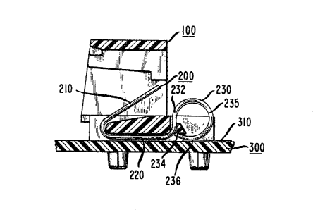
As seen most clearly in FIG. 4, each spring contact 200 comprises a linear
contact portion 210 at one end that is joined by an intermediate portion 220 to
a loop contact portion 230 at the other end. The linear contact portion 210
extends cantilever-fashion within th cavity 112 of the housing portion 110 of
support member 100 and serves to make electrical connection with a
corresponding contact of a mating plug (not shown). The intermediate portion
220 extends within one of the grooves 125 in the bottom surface 122 and the
associated slot 123 in the front end of the base portion 120 and serves to
generally locate the linear contact portion 210. The loop contact portion 230 islocated within the portion of th base portion 120 to the rear of the housing
portion 110 and serves to engage and make solderless electrical connection with
a conductive path 310 on an associated printed circuit board shown in FIG. 5.
The loop contact portion 230 includes a first end region 232 and a second
end region 234. The first end region 232 joins the loop contact portion 230 withthe intermediate portion 220 and is situated within the opening 126 in the base
portion 120 to the rear of the groove 125 within which the intermediate portion
is situated. The second end region 234 of the loop contact portion 230 extends
adjacent to the first end region 232 and is accommodated by the groove 130 in
the bottom surface of the base portion 120 to the rear of the opening 126 withinwhich the first end region 2332 is situated.
The remainder of the loop contact portion 230 comprises a main region
235 that i8 partially accommodated within the slot 124 in the base portion 120
that is to the rear of the groove 127 in which the second end region 234 is
accommodated. The main region 235 extends below the bottom surface 122 of
the base portion 120 and includes an arcuate contact surface 236 which is
adjacent to the second end region 234. The contact surface 236 provides the
site of engagement with the conductive path 310 on the printed circuit 300
~I.X'7
- 6 -
(FIG. 5).
As a result of the foregoing arrangement, the loop contact portion 230 is
restrained in a lateral direction between the sides of the slot 124 at the base
portion 120. In addition, both the first and second end regions 232 and 234 of
5 the loop contact portion 230 are restrained in a direction generally normal tothe site of engagement of the arcuate contact surface 236 with the conductive
path 310 on the printed circuit board 300. The main region 235 of the loop
contact portion 230, however, is free to be deflected in this direction and, as
shown in FIG. 5, when pressed into engagement with the conductive path 310,
10 the main region essentially rotates abut the first and second end regions 232 and
234.
This deflection occurs when the connector is mechanically mounted to
the printed circuit board 300 by means of four cylindrical locking posts 127.
The posts 127 extend downwardly from the bottom surface 122 of the base
15 portion 120, and the posts are accommodated by holes (not shown) in the
printed circuit board 300.
As shown most clearly in FIG. 2, each post 127 includes an upper portion
128 having a diameter that is slightly less than the diameter of the hole that
accommodates it and having a height slightly greater than the thickness of the
20 printed circuit board 300. In addition, each post includes a lower portion 129
having a diameter somewhat larger than the hole in the printed circuit board
300. Finally, each post 127 is split longitudinally whereby the sides of the lower
portion 12~ can be deflected inwardly to permit it to pass through the
accommodating hole and then return to an undeflected state when the upper
25 portion 128 is positioned within the hole. The lower portion 12~ of each post127 thereby serves to secure the connector to the printed circuit board 300.
Referring now to FIG. 6, the force-deflection diagram shown there depicts
the deflection of a single loop contact portion 230 in the process of the
connector being secured to the printed circuit board 300. That is, it depicts the
30 deflection of the loop contact portion 230 from its position in FIG. 4 to itsposition in FIG. S. As the locking posts 127 are pushed downwardly through
the accommodating holes in the printed circuit board 300, the deflection of the
loop contact portion 230 is increased. This deflection reaches its maximum
when the bottom surface 122 (FIG. 4) engages the upper surface of the printed
- 7 -
circuit board 300.
Once the connector is in place with the lower portion 129 of each locking
post 127 returned to its undeflected condition, the downward insertion force is
removed from the connector, and the force exerted by the loop contact portion
5 230 against the printed circuit board 300 moves the connector upwardly until
the upper end of the lower portion 129 of the locking posts 127 engages the
underside of the printed circuit board 300. This takes up any tolerance
variation between the thickness of the printed circuit board 300 and the height
of the upper portions of 128 of the locking posts 127. The deflection of the
10 loop contact portion 230 is thereby slightly reduced. But the loop contact
portion 230, because of the above-described manner in which the spring contact
200 is supported on the support member 100, retains a spring loading in excess
of 1.5 pounds. This force provides the contact force necessary to produce a
good solderless electrical connection to the conductive path 310 on the printed
15 circuit board 300.