Note : Les descriptions sont présentées dans la langue officielle dans laquelle elles ont été soumises.
9118
TI~LE ED-0355
Bus Structure Having Con~tant
Electrical Characteri6tic
5 BACKGROUND OF THE INVENTlON
Field of the Invention The pre~ent
invention ~elate6 to a hiqh speed data communications
~- ~ystem and in particular to a transceiver mounting
arrangement for such a sys1;em.
De6criDtion of the Prior Art In high 6peed
data communication~ systam~ using computar6 it i8
recognized that the electrical characteriRtic6 of the
signal path6, or "buses", interconnecting variou6
circuit ~odules of the sy6tem become inc~easingly
critical as tran6mis6ion rates increa~e and as logic
tran~ition time6 decrease. The6e bu~es, whether
~ realized as trace~ on a circuit board, coaxial
_ cable~, twi6ted pairs or individual wire6, mu6t be
gon6idered a6 tran6mi6sion line6. To achieve
error-free. high ~peed dig;tal transmi~6ion-the
transmis6ion line6 mu6t exhibit certain propertie6:
uniform characteri6tic impedance ~which require6
uniform geometry) along their length: o~ti~um
characteri6tic i~pedance con6istent with current
sourcing capability of the driving circuit elements:
proper termination6 at the end~ to prevent
reflection6; and high propagation veloci~y.
In the ~ypical ~y6tem the main system bus ~6
~ 30 dispo~ed on a buc support sub6trate called a
i "motherboard" and the con6tituent modules of the
6ystem are di6po6ed on ~eparate dedicated support
sub6trate6, or "daughterboards". The overall data
proce6sing system is configured by phy6ically
~5 interconnecting the daughterboard6 with the
._ _
.
79~8
motherboard. The requi~ite properties of the main
bu6 on the motherboard are adver6ely affected when
daughterboards are removed from or added thereto.
In an attempt to minimize effect6 on the
properties of the main bu6, high input impedance
tran~ceiver6 are located on the daughterboard near
the point at which it is received by the
motherboard. However, the tran6ceiYer it6elf, a6
well a6 the "~tub" or b~anch conductor through which
the tran6ceiver i6 interconnected to the bus, i~pose6
non-negligible impedance and capacitive load6 on the
bu6. These loads tend to change the propertie6 oP
the bu6 when daughterboa~d6 are added or removed.
For example, when daughterboard6 are pre6ent the
effective impedance of the bus is lowered.
Acco~dingly, precise termination of the bu6
(nece66ary to prevent 6ignal reflections) i6
difficul~ to maintain.
Change~ in the bus impedance cau6ed by the
ab~ence or presence of transceivers along a bus are
addre66ed by United States Patent 4,475,191. In
accordance with thi~ patent where daugh~erboards are
pre6ent the bus is terminated in a fir6t impedance.
Where ~he daughterboard6 are ab6ent the bu6 is
terminated in a 6econd, higher, characteri6tic
impedance. In addition a current driver with a
deliberately lengthened ri6e time i6 u6ed. Such a
601ution to the impedance matching problem, however,
impo~e6 limitation6 on the speed of operation and
upon the transitio~ ~ime between logic level6.
The impedance and capaciti~e load6 impo~ed
on the bu6 by the ~tub6 i6 recognized in t~e Hotorola
MæCL De6ign Handbook. Thi~ reference work define6
limitation6 on bu6 propertie6 in relation to the
number and length of the 6tub~ and place6 upper
t~ll8
-
limit6 on the length of the 6tubs in order to hold
the effec~6 of the 6tub~ within tolerable limits.
In the related technology of local area
network6, a~ typified by the Ethernet (TM) network,
S the propertie6 of the coaxial cable bu6 u6ed therein
are maintained a6 constant aE; po66ible by utilization
of transceiver6 mounted in cable tap unit6 which are
attachable along the bus. In 6uch sy6tem~ the
tran6ceiver6 are typically contained within the cable
tap unit and are connected to the coaxial cable at
de6ignated location6 by meanE; of an in6ulatio~
piercing connector arrangement. When the cable tap
unit i8 removed the tran6ceiver and connector are
removed a 8 well.
In view of the foregoing it i~ believed
advantageous to provide a communications bus that
exhibits preci6ely determinable impedance and time
delay characteri6tic~ and that maintain6 the6e
characteri6tic~ regardle66 of the presence or ab6ence
of a660ciated circuit modules connected to the bu6 at
all of the tran6ceiver arrays provided for that
purpo6e .
SUMMARY OF THE INVENTION
The pre6ent invention relate6 ~o a~
electronic 6y6tem Aaving a high 6peed communication~
bus exhibiting i~proYed ~erformance characteri6tic~
while retaining the practical convenience of
configuration ~lexibility and modulari~y. The bu~ i~
phy6ically di6posed on a bu6 6upport sub6trate wit~
as60ciated electronic circuit module6 being
po6itioned on separate 6upport 6ub6trate6. The
circuit module6 are removably connected to the bu6
6upport 6ub6trate and communicate with the bu6
through tran6ceiver array6.
:. .
118
In accordance with the pre6ent invention the
tran~ceiver array6 are phy~ically di6po~ed on the bu6
~upport 6ubstrate with the minimum connection length
being defined between the bu~ and each tran6ceiver
array. A~ a result of thi6 l~tructural arrangement
the impedance and time delay characteristic6 of the
bus remain 6ubstantially constant and are unaffected
by placement or removal of functional circuit modules.
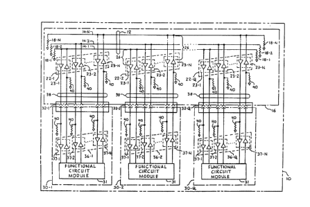
BRIEF DESCRIPTlON OF THE DRAWINGS
The ~igure i8 a 6tylized pictorial and
6chematic repre6entation of an electronic data
communication6 6y6tem having a bu~ tran6ceiver
arrangement po6itioned in accordance with the
teaching~ of the pre~ent invention.
DETAILED DESCRIPTION 0~ THE INVENTION
Referring to the Figure shown i~ a 6tylized
pictorial and ~chematic representation of a high
~peed data communication6 6ystem 10 of the type able
to facilitate the rapid transfer of data between
functional element6 of a data proce6sing system. The
data communications sy6tem 10 may ~ind particular
utility in connection with the tran6f~r of large
block6 of graphics or image data, such as that
produced by a medical imaging system.
The sy6tem 10 includes a bUB 12 formed of a
plurality of individual ~ignal conduction path6 14-1
through 14-N. The paths are di6posed on the 6urface
30 oF or embedded within a ~uitable bu6 support
6ubstrate, or "motherboard", 16. Any convenient
number of conduction path6 i~ provided consi~tent
with the word width of the data being proce66ed and
with sy6tem control needs. Each conduction path 14-1
through 14-N is terminated at each end with it6
1~'79~18
respective matching characteri~tic impedance 18-1
through lB-N. The termination impedance6 18 ~erve to
prevent the generation of ~ignal reflection6 back
along each conduction path 14. The values o the
impedance6 18 are determinable when the motherboard
16 i8 a~embled and are selected to preci6ely match
the characteri6tic impedance of the conduction path
14. The bu6 12 al60 exhibits determinable time delay
characteristic6 which are a function of, among other
things, the dielectcic constant of the material of
~ the 6ub~rate 16 and the length, geometry and
phy6ical proximity of the individual conduction path6
14, a~ will be readily appreciated by tho6e ækilled
in the art.
A predetermined number of tran6ceiver array~
22-1 throuqh 22-Q are di6tributed along the bu6 12
with a predetermined 6pacing being defined between
each transceiver array. Each tran6ceiver array 22
include6 transceiver element6 23-1 through 23-N.
Each tran6ceiver element 23 i6 electrically connected
to it6 as60ciated conduction path 14 of the bu~ 12 by
a predetermined length 26 of conductor, commonly
referred to a6 a "stub". The term stub i6 harein
u6ed to refer to that lengtb 26 of conductor branching
from a given conduction path 14 of the bu6 12 to some
active or pas6ive circuit element, in this ca6e the
amplifier of the ~ran6ceiver element 23. Suitable
for u6e as each tran~ceiver element 23 i6 an
integrated circuit package such a6 those manufactured
by Fairchild Camera and Instrument Corp~ration and
601d under model number F100194. A6 u6ed herein the
length 26 of the ~tub includes not only the length of
the conductor6 external to the tran6ceiver package
but alço the length of the electrical leads which are
Z7gl~L8
part of the integrated circuit package. This total
length is typically not mo{e than 0.25 inche~ for
reasons which shall be discussed hecein.
The elements of the data communication6
~y6tem 10 are formed as functional circuit modules 31
disposed on separate ~upport 6ubstrates 30-1 to
30-Q. Such ~ubstrates are commonly called
"daughterboard6". These daughterboards are typically
connected to the motherboard 16 via respective
suitable multi-pin electrical connector6 32-1 to
32-Q, al~hough other ~uitable connection means may,
of course, be u6ed. ~ach of the funceional circuit
module6 31 orl t~e daughterboards 30 communicates with
the bu6 12 through a dedicated transceiver array 22.
Moreover, each of the daughter boardc 30 i6 removably
connectable to the motherboacd 16 thus providing
flexibility in configuring the data communications
6y6tem 10.
Each of the dauqhterboard6 30 carrie6 a
sepaeate array 36 of transceiver element6 37 6imilar
to the tran6ceiver elements 23. The group of
conductor6 di~posed between each transceiver array 22
on the motherboard 16 and each transceiver array 36
on the daughterboard 30 define a secondary bus 38.
This 6econdary bu6 38 obviates the need for crowding
the transceiver array 36 along the edge of the
daughterboard 30 and in the vicinity of the connector
32 as60ciated with that board as i~ typically
pra~ticed in the prior art. In the Figure the
6econdary bu6 3~ i6 comprised of a plurality of
unidirectional conduc~ion path~ each connecting an
associated tcansmitter of one tcan~ceiver element to
an as60ciated receiver of another tran6ceiver
element. Each conduction path of the secondary bus
35 is appropriately terminated at i6 receiving end by
it6 characteristic impedance 40.
791~3
The 6tructural arran~ement in accordance
with the present invention, wherein the transceiver
array~ 22 are phy~ically di6po~ed on the motherboard
16, provides beneficial advantage6 over the system6
of the prior art. Placement of the transceiver
arrays 22 on the motherboard 16 effectively 6horten6
the length 26 of the stub~. A6 a result the ~ignal
reflection delay from the stubs i6 alway~ 6ho~ter
than the ri6e time of even the fa~te6t logic
familie6, such a6 ECL and GaAs.
In addition, change~ in the impedance and
propagation delay of the bu~ 12 due to removal or
insertion of daughterboards 30 are avoided. In the
present system these parameter~ remain substantially
con6tant, regardle66 of the presence or absence of a
daughterboard 30 at a given connector 32. This i8 SO
because the tran6ceiver arsay6 22 always remain in
place on the motherboard 16 and are not removed or
added when a given daughterboard 30 i8 removed or
added. Each conduction path 14 of the bus 12,
therefore, is always presented with the impedance of
the associated transceiver element 23 and it~ ~tub
26. It i~ thus po6sible to select termination
impedances 18 that precisely match the characteristic
impedance of the re6pective conductio~ path 14.
Thos2 ~killed i~ the art, ~aving the benefit
of the present invention a6 hereinabove described,
may ef~ect numerou6 modificaeions thereto. It i6 ~o
under~tood, however, that the6e and other
modifications lie within the contemplation of the
present invention, a6 ~et forth in the appended
claim6.