Note : Les descriptions sont présentées dans la langue officielle dans laquelle elles ont été soumises.
3~7~
- 1 - 5644~-355
The present invention relates to a semiconductor laser
and, more particularly, to a semiconductor laser device which
oscillates with a single longitudinal mode and has a continuous
wavelength tuning capability.
The background of the invention and the invention itself
are illustrated in the accompanying drawings, in which:
FIG. 1 is a section of a semiconductor laser device
embodying the present invention;
FIG. 2 is a section of a prior art wavelength tunable
DBR laser;
FIG. 3A is a plot useful for e~plaining -the principle of
operation of the prior art tunable DBR laser and showing a rela-
tionship between wavelengths and phases eR f light which is
; returned from a tuning region to the boundary between the tuning
region and an active region and phases e~ of light which is retur-
` ned from the active region, and a relationship between the phases
e~ and reflectivity with the tuning region looked into at the
boundary, and
FIG. 3B is a plot for demonstrating -the principle of
~0 operation of the present invention and showing a relationship
between wavelengths and phases e~ and e~; and
FIG. 4 is an illustration of an alternative embodiment
of the present invention.
As well known in the art, a distributed feedback (DFB)
or distributed Bragg reflector (DBR) semiconductor laser oscil-
'.; lates with a stable single longitudinal mode even during high-
:```
:.
,t
"1~
, .
.~ .
7~
- la - 66446-355
- speed modulation utilizing wavelength selectivity of a diffraction
. grating which is provided in a semiconductor crystal. With such a
- merit, a DFB or DBR laser is deemed to offer a hopeful light
source for
` :
.` ~
~` ~
--2--
future optical coherent transmission systems as well as for long
distance, large capacity optical fiber communications. In an opti-
cal heterodyne system which is one of the optical coherent trans-
mission systems, it is a primary requisite that at a receiving sta-
tion a beat signal having a predetermined frequency be provided by
interference between incoming signal light and light which is oscil-
lated by a local oscillation light source, or local oscillator. To
meet this requisite, the local oscillator has to constantly follow
the wavelength of signal light while maintaining a certain predeter-
mined
.
.
~`
'~` ' '
i~
'~. ' ~ ' .
---2--
frequency difference. Therefore, a laser which is to
serve as a local oscillator needs to oscillate with a
single longitudinal mode and, yet, feature wavelength
controllability, in particular continuous wavelength
controllability.
Wavelength-controllable, or tunable, single~wavelength
semiconductor lasers include a DBR laser which was reported
in "Bragg Wavelength-Tunable DBR-DC-PBH LD" (in Japanese)
1984 National Convention (Record) of the Institute of
Electronics and Communication Engineers of Japan, Part 4,
Paper No. 1022. A schematic structure of this turnable
DBR laser is shown in FIG. 2. As shown, an active layer 3
having a 1.3 ~m wavelength composition and a P InGaAsP
guide layer 2 having a 1.2 ~m wavelength composition are
sequentially grown on an n-InP substrate 1. A diffraction
grating 10 having a period of about 4000 A is provided
`~ only in that part 15 of the surface of the guide layer 2
which serves as a tuning region, while that part 16 of
the guide layer surface which serves as an active region
is left flat. Thereafter, a p-InP cladding layer 4 and
a p+-InGaAsP cap layer 5 are sequentially grown on the
entire surface of the guide layer 2. Provided above the
tuning region 15 and the active region 16 are a tuning
electrode 6 and a laser driving electrode 7, respectively.
The cap Layer 5 is partly removed to define a groove 11
,.
~i~
.
between the electrodes 6 and 7 which insures electrical
isolation between the electrodes 6 and 7. An n~electrode 9
is provided on the n-side of the multi-layers semiconductor.
The DsR LD having such a structure oscillates with a single
longitudinal mode when a drive current Id is injected
into the active region 16, the wavelength being tunable
responsive to a tuning current It injected into the tuning
region 15. This is derived from the fact that the current
It injected into the tuning region 15 increases the carrier
density at the tuning region 15 side and, thereby, lowers
the refractive index through the plasma effect, with the
~esult that the Bragg wavelength which is dependent upon
the period of the diffraction grating 10 is shifted toward
shorter wavelength. Therefore, injection of the current It
causes the oscillation wavelength to vary toward shorter
wavelength. However, the tuning characteristic particular
to this kind of DBR LD involves mode jumping. Specifically,
the DBR LD is incapable of performing continuous wavelength
tuning although capable of controlling the Bragg wavelength
by means of the tuning current It, because it fails to
control the phase of light which, wlth the active region 16
viewed from the boundary between it and the tuning region
15, is propagated thxough the active region 16 and then
returned by reflection from the right end of the LD.
:
.
,
- 5 - 66446-355
Summary of the Invent;.on
It is therefore an o~ject o-f the presen~ invention to
provide a semiconduc~or laser device which oscilla-tes with a
single longitudinal mode and is capable of continuous wavelength
tuning.
According to one aspect, the present invention comprises
a multi-layer semiconductor structure including an active region
which includes an active layer of emitting light responsive to
stimulation and a cladding layer on said active layer, a first
control region including a guide layer for guiding light which is
being propagated, and a second control region including a guide
layer provided with a diffraction grating for guiding light which
is being propagated, said active region, first control region and
second control region being arranged in a row along an axis of
resonance, said cladding layer extending to and overlying said
; guide layers of said first and second control region; an active
electrode adapted to inject a current into the active region; a
` first control electrode and a second control electrode adapted to
inject currents, respectively, into the first and second control
~0 regions; means for applying a drive current to said active elec-
trode; and means for applying control currents to the first and
second control electrodes in a predetermined ratio, and said
active regionj first control reyion and second control region
being supplied with forward currents with respect to PN junctions
formed in said active, first and second control regions.
~ `
~` ` '
~ , , .
,
-5a- 66446-355
means for applying control currents to the first and
second control electrodes in a predeterm.ined ratio, and said
active region, first control region and second control region
being supplied with forward currents with respect to PN junction
to produce injected carrier~
i
.
~ ,
`.` `~.J
`i` , . , :
' . '
'':, ', ' ' ' ' ' '
'~ ' ' '' '`' ' ` ,' .
~ ' .
L~
- 6 -
The phase condition for the element shown in Fig. 2
to oscillate is provided as ~ + e r - 2 m h, where ~ is
a phase of light returned from the tuning region 15 due
to reflection with the tuning region 15 viewed from the
boundary between the tuning region 15 and the active
region 16, ~7 is a phase of light returned from the
active region 16 as viewed from the boundary, and m is
an integer. Assuming that the active region 16 extends
over a length L, and that the propagation constant is B,
the phase ~r is represented by a r = -2 ~ L. The wavelength
dependency of the phase ~ and (2m~ ) is shown at left
of FIG. 3A. The phase ~ is variable continuously with
` the amount of current injection into the tuning region 15
; as a parameter. The curves indicated by a solid line,
broken line and dash-and-dot line are associated with a
case wherein the amount of current injection is increased.
Meanwhile, the phase ~ r is immune to changes in the amount
~` of current injection into the tuning region 15. The above-
stated oscillation phase condition are represented by the
` 20 crossing points of ~ and~(2m~ - ~ r); possible oscillation
modes are A, B and C as shown in FIG. 3A. Shown at right
of FIG.3A is the ~ dependency of reflectivity with the
tuning region 15 looked into from the boundary. The
specific wavelength which provides ~ /2 coincides
~' 25 with the Bragg waveléngth and, under this condition,
~, .
'
'. '' ,
-- 7
the reflectivity at the tuning region 15 side becomes
maximum. The actual oscillation mode is a mode having
the highest reflectivity out of those modes which satisfy
the oscillation phase condition. Stated another way,
among the modes A, s and C, one whose phase ~ is closet
to ~/2 oscillates; before the tuning current It is applied
(It = 0), the mode A will oscillate. Upon injection of
the current It, the Bragg wavelength shifts toward shorter
wavelength due to a decrease in refractive index which is
derived from the plasma effect, causing the curve
representative of ~ to shift in parallel toward shorter
wavelength. As a result, the mode represented by the
crossing point A shifts little by little toward shorter
wavelength as A -~ A' ~ A" responsive to the increase
in the current It while, at the same time, the phase 9~
of mode A shifts away from ~/2. In contrast, the mode B
which neighbors the mode A at the shorter wavelength side
varies as B -~ B' -~ B" responsive to the increase in
current It, the phase 0~ approaching ~/2. It follows
. 20 that a condition wherein the phase ~ of the mode B is
closer to ~/2 than that of the mode A occurs at a certain
injection level of the current It, allowing the mode to
jump as represented by A' _~ B' in FIG. 3A. In this
manner, ~n a tunable DBR laser with the prior art
structure, mode ~umping is repeated as A -~ B ~ C
: '
`
- ,
~ 2~
- 8 -
responsive to an increase in the current It so as to
` undesirably shift the wavelength toward shorter wavelenyth.
In order to accomplish continuous waveform tuning
which is free from mode jumping, the present invention
provides a structure in which the phase ~ r of reflection
is controllable at the end of the laser on the active
region 16 side. Specifically, a phase control region
which utilizes variations of refractive index due to the
plasma effect is added next to the active region 16,
; 10 so that ~ r may be intentionally controlled by injecting
a phase control current into the phase control region.
FIG. 3B shows the principle of operation of the
present invention for continuous wavelength tuning.
Continuous wavelength tuning is attainable while
maintaining mode A oscillation, by shifting the ~ and
(2m~ ~ ~ r) phase curves in parallel by a same amount
toward shorter wavelength such that the phase ~ of the
mode A constantly remains at ~12. It follows that
continuous waveIength tuning will be enabled if a tuning
current and a phase control current are injected at the .-
same time to equalize the amounts of shift of the 0~ and ~r.
.
Detailed Descrip-tion of the Preferred Embodiment
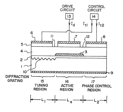
Referring to FIG. 1, a semiconductor laser device in
;
~ accordance with the present invention is shown and includes
!~ 25 an n-InP substrate 1. The n-InP substrate 1 is provided
; ~ :
t;
:
'
' . . .
,
.~ '
- 9
with a diffraction grating 20 in a part thereof which
corresponds to a tuning region 15, the diffraction
grating 20 having a period of 2400 A. An n-InGaAsP
guide layer 2 having a 1.3 ~m wavelength composition and
an active layer 3 having a 1.55 ~m wavelength composition
are sequentially grown by epitaxy on the entire surface
of the substrate 1 inclusive of the diffraction grating 10.
Then, the active layer 3 is removed except for a part
thereof which covers a particular region which will serve
as an active region 16. A phase control region 17 is
provided at the other end of the laser remote from the
tuning region 15. Thereafter, a p-InP cladding layer 4
and a p+-InGaAsP cap layer 5 are sequentially grown by
epitaxy over the entire surface of the multi-layers
semiconductor. This is followed by providing a tuning
electrode 6, an active electrode 7 and a phase control
electrode 8 in their associated regions 15, 16 and 17,
respectively. Grooves 11 and 12 each being deeper than
the cap layer 5 intervene respectively between the
electrodes 6 and 7~and between the electrodes 7 and 8
in order to set up sufficient electrical isolation. An
n-electrode 9 is provided on the u~derside of the sub-
strate 1. An electric circuit 13 is connected to the
active electrode 7 of the so constructed semiconductor
laser to inject a drive current Id for driving the laser.
.
:
~ :'
' .
~ 10 -
Connected to the tuning electrode 6 and phase control
electrode 8 is an electric circuit 14 which is adapted
to inject a tuning current It1 and a phase control
current It2 at the same time in such a manner that their
ratio It1/It2 remains constant.
In the semiconductor laser device constructed as
described above, the laser oscillates with a single
longitudinal mode around the wavelength of 1.55 ~m when
the drive current Id is injected into the active region 16.
For continuous wavelength tuning, it is necessary that the
. phase curves of ~ and ~ shown.in FIG. 3B be shifted by
a same amount toward shorter wavelength responsive to the
.~ currents It1 and It2, thereby causing the mode at the
crossing point A to constantly maintain 0~ =~ /2. The
~` 15 amount of horizontal shift of the phase curve 0~
;~' is equal to the amount of shift of the Bragg wavelength
and, by using an effective refractive index n1 and a
~ refractive index variation ~ n1 of the tuning region 15,
.` is expressed as:
n1
` 20 ~11 = n 1 0 ............................. Eq. (1)
where lo is the oscillation wavelength before injection
' of the current It1.
` Meanwhile, the amount of shift ~12 of the phase
curve of (2m~ - 2~L) is produced by:
~`
~,
;.
i ,. . .. .
: . .
,~. ' ~ ' ' ' , :
~. :. . .
,~: . .
.: .
' ' ' ' : ~:
'7.~
-- 11 --
~ ~2 n L + n L ~ O .......................... Eq. (2)
:,
From the above, it follows that ~1 and a~ 2 become
equal to each other under the following condition:
nl ~ n2L2
nl a a 2 2 .... Eq. (3)
Assuming that the effective refractive indices of the
respective regions are substantially the same (n1 - n2 = na)'
the Eq. (3) may be written as:
nl = L + L2 ~ 2 .... Eq. ~4)
~` Further, since the refractive index vatiation due to
current injection is proportional to the square root of
an injection current density, the Eq. (4) may be method as:
`:
J L1 ~ ~ .... Eq. (`5)-
.
where L1 is the length of the tuning region lS.
As seen from the above, the prerequisite for continuous
;~
tuning is that ehe curr~nts, It1 and It2 be injected in
:~ :
.
, ,, , :
Lg~
-- 12 --
such a manner as to satisfy the following condition:
It1 = ~ ) ' L1 ,... Eq. (6)
' 1
` In will be understood from the above description
that the semiconductor laser device in accordance with
the present invention is tunable in a continuous fashion
by injecting control currents It1 and It2 respectively
into the tuning region 15 and the phase control region 17
such that the Eq. (6) is fulfilled.
Experiments showed that the semiconductor laser device
of the present invention realizes continuous wavelength
tuning of about 40 A at the wavelength band of 1.55 ~m.
Also, a light output as great as about 5 mW was achieved
which promotes the application of the device as a local
oscillation light source of an optical heterodyne system.
While the present invention has been shown and
described in relation to a semiconductor laser device
which oscillates with a wavelength of 1.55 ~m, the lasing
wavelength is not limited thereto. For example, a tunable
semiconductor laser device which oscillates with the
wavelength of~1.3 ~m may be provided by selecting a 1.2 ~m
wavelength composltion for the guide layer 2 and a period
of 2000 A for the dlffraction grating 10.
~: :
.
.i . .
' ' ~ ,. ' ~,
.", , ~ ~ .
- 13 - 664~6-355
The guide layer 2 which is positioned below the active
layer 3 in the illustrative embodiment may alternatively be provi-
ded above the active layer 3, in which case the diffraction grat-
ing 10 will be provided between the gulde layer 2 and the cladding
layer 4. In addition, a thin InP layer may be formed between the
guide layer 2 and the active layer 3.
Although the active reqion 16 in the illustrative
embodiment is located at the center of the laser, the respective
regions may be arranged in any other suitable configuration such
as with the phase control region 17 located at the center as shown
in Figure 4.
In the illustrative embodiment, the active layer 3 is
removed in the tuning region 15 and phase control region 17. If
desired, however, the active layer 3 may be left in all the three
`~ regions.
; While the means for enhancing electrical isolation
between electrodes are implemented by the grooves 11 and 12 which
are deeper than the cap layer 5, it may alternatively be implemen-
ted with, for example, implantation of protons to between the
~0 electrodes. The semiconductor applicable to the present invention
is not limited to InGaAsP/InP and may be replaced with
` AlGaAs/GaAs, for example. Further, the ratio of the control
currents Itl and It2 does not always have to
`. ~''
.
. . .
- 14 -
satisfy the Eq. (3) and needs only to be close to a
condition which fulfills the Eq. (6).
In summary, it will be seen that the present
invention provides a semiconductor laser device which
wavelength is tunable in a continuous manner. The device,
therefore, implements not only a local oscillator for an
`~ optical heterodyne system but a wide range of other light
sources utilizing its inherent tunability, such as a light
source for frequency modulation schemes, a light source
" 10 for transmission in a frequency shift keying (FSK)
heterodyne system which belongs to a family of optical
; heterodyne systems, and a light source for wavelength
multiplex transmission.
,`
~ ,
:: ~
~' ` ,
'`,' ' ',
~ .
~, , .