Note : Les descriptions sont présentées dans la langue officielle dans laquelle elles ont été soumises.
~ 2~
.. .
-- 1 --
This invention generally relates to
methods and apparatus for ink jet printing and
plotting but more particularly this invention
relates to the field of high resolution ink jet
color printing and plotting.
US-A-3,916,421 descrlbes an ink jet
recording device in which an ink jet issues under
high pressure from a nozzle and breaks up into a
train of drops ac a point of drop formation inside a
control electrode. This train of normally uncharged
drops travels in a line or along an initial axis
toward a recording medium, as paper, which is
mounted on or otherwise affixed to a moving support,
e.g. a rotating drum of a drum plotter. On the way
from the nozzle toward the paper, the drops pass a
transverse electric field generated between a
negatively charged high voltage electrode and a
lower part of the control electrode. Now, if a
positive control voltage is applied to the control
electrode while the ink in the nozzle is grounded,
an electric field is established at the point of
drop formation causing each of the drops ~ormed at
the point of drop formation to be negatively
charged. Because of the charge, these drops are
deflected into a catcher and cannot reach the
recording paper. Thus, the length of time during
which the signal voltage or "print pulse" applied to
; the control electrode is zero or less than a cut-off
control voltage, determines the number of drops that -
reach the elementary area (pixel) of the recording
paper, which is aligned with the ink jet axis.
Thus, the prln-ting pulses control the amount of ink
'; .
: .
. . .
:
.. . .
~28~9~
-- 2 --
laid down at the individual pixels and -therefore the
densities of -the pixels which in turn may ~orm a
halftone image.
An improvement of the ink jet apparatus
mentioned above is described in US-A-4,620,196. In
this improved ink jet apparatus, the rate and
position of drop formation is controlled by ultra-
sonic stimulation. Further, the length of the
electrical print pulse determining the number of
drops that reach the recording medium is adjusted
such that it equals n/f, where f is the drop
formation rate which is equal to -the ultrasonic
stimulation frequency (e.g. 1 MHz) and n is an
integer chosen such that the ratio n/f is close to
the length of the original print signal. Addition-
ally, the start of the print pulse is synchronized
with a suitable phase of the ultrasonic stimulation.
This insures that the start of the print pulse
always coincides with the same phase of the drop
formation process. The effect of these measures is
an appreciable reduction of the graininess of the
halftone image formed by the printed pixels.
We have found that the graininess of the
printed image can be~ further reduced by synchroniz-
ing the drop formation rate and, thus, the printing
pulses, with the pixel rate.
In the known ink jet apparatus, the source
as an oscillator, which produces the ultrasonic
stimulation signal which is also used as clock
signal for the system is generated entirely
independent of the pixel signal which determines the
location of the subsequent~pixels recorded on the
record medium. ~ We have found that this indefinite-
ness of the relation between the stimulation or
~ :A :: ~
, .. ... . . .... . . .. . . . .. . . .
~6g~~
- 2a -
clock signal on the one hand and the pixel signal on
the other hand is a cause for the s-till remaining
graininess of the image. Thus, according to the
present invention, the stimulation or clock signal
and the pixel signal are coordinated or synchronized
for further reducing the graininess of the image.
In accordance with the invention there is
provided an ink jet printing method wherein a record
is produced by applying varying amounts of ink on a
plurality of pixel locations of a record medium,
said method comprising the steps:
(a) generating an ink jet directed towards
said record medium, said ink jet breaking
up into a series of drops with a pre-
determined drop formation rate,
(b) applying an electric charge of predeter-
mined magnitude to selected drops,
(c) deflecting each charged drop as a function
of its charge to determine whether the
drop travels along a recording path to
reach said recording medium or is
intercepted,
: (d) producing relative transverse movement
between said drop path and said recording
medium,
(e) generating a first signal indicative of
the drop formation rate,
(f) generating a second signal from relative
movement, the second signal being indi-
~; 30 cative that pixel position on the record
: medium is aligned with said drop path,
(g) deriving a density value for the aligned
: pixel position in response to said second
signal,
:: :
~:~A
; : : - .. . ...
... - . . . ,. . .. . . . . , ` .. .
... ~.. , ~ .... . . ... ... . . .. .. , . ,- .` .
~2~
- 2b -
(h) generating a print pulse signal of pre-
determined length between leading and
trailiny edges in response to said derived
density value and said first signal, said
S density value controlling -the length and
said first signal controlling the time of
occurrence of the leading edge of said
print pulse signal,
(i) controlling said charging step (b) by
means of said print pulse signal,
-the improvement consisting in
(j) combining said first and second signals to
establish a non-coincidental time
relationship between the time at which
said density value deriving step (g)
occurs and the time when the leading edge
of the print pulse occurs.
Also in accordance with the invention
there is provided an ink jet printing apparatus
wherein a record is produced by applying various
amounts of ink on a plurality of pixel locations of
a record medium, said apparatus comprising:
(a) means for generating an ink jet directed
towards said record medium, said ink jet
breaking up into a series of drops with a
: . predetermined drop formation rate,
(b) means for selectively charging said drops,
(c) means for applying a deflecting force to
: each :charged drop as a function of its
- charge to determine whether the drop
travels along a recording path to said
.
record medium or is intercepted by inter- .-
cepting means, :
`.A , ~ , ,
- . , . - . - ~ ~
, .. , , "
- ~' ' :: ~ . .
:: : : : :. . ,
~L2~6911
(d) means for producing relative movement
between said path and said record medium,
(e) means for generating a first signal indi-
cative of said drop formation rate,
(f) means for generating a second signal
depending on said relative movement, the
second signal being indicative that a
pixel position on said record medium is
aligned with said path of said drops which
read said record medium,
(g) means for deriving a density value for the
aligned pixel in response to said second
signal,
(h) means for generating a prin-t pulse signal
having a predetermined length between
leading and trailing edyes in response to
said derived density value and said first
signal, said density value controlling the
length and said first signal controlling
the time of occurrence of the leading edge
of said print pulse signal,
the improvement consisting in
(i) means for combining said first and second
signals to establish a non-coincidental
time relationship between the time at
which said density value is derived and
the time at which the leading edge of said
print~pulse signal occurs.
In a preferred embodiment, a digital pixel
density signal, generally a color component pixel
density signal, is loaded into a down counter by the
pixel signal. The down counter lS then clocked down
to zero by the clock cignal to determine the number
of ink drops
: ~'
:
::
~ . . . .
applied to the respective pixel. A clock/pixel signal synchronizing
circuit secures that the load pulse which is derived from the pixel
pulse and effects the loading of the density value into the down
counter, falls between the effect;ve, e. 9~ rising edges of two
subsequent clock pulses which clock the down counter. of course, any
other suitable digital-to-pulse length converter may be employed
instead of a down counter.
Many other advantages, features and additionaL objects of the
present invention will become apparent to those skilled in the art
upon making reference to the following detailed description and the
accompanying drawings, in which preferred embodiments incorporating
the principles of the present invention are shown by way of
illustrative examples.
In the draw;ngs:
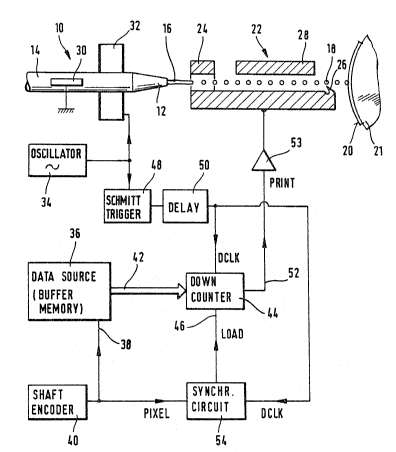
Fig~ 1 shows a simplified side view of a part of an ink jet pr;nter,
partially in section, and a block diagram of an associated
electrical circuitry which incorporates the present inven-
tion,
: ' .
Fig. 2 shows a circuit diagram of a clock signal/pixel signal
- synchronizing circuit according to a preferred embodiment of
the ;nvent;on
Fig. ~ sho~s waveforms of signals occurring in the circuits of Figs.
I and 2 to which reference is made when expla;ning the
conf;guration and operation of the synchroniz;ng circuit.
F;g~ 4 shows a c;rcuit diagram of an alternat;ve synchronizing
c;rcu;t.
-
.
.,
:
:~ ,
: :
.. . , ~ , , ., , . , ,, , ~ . :
. . .
. . , : ,: , ., . :- , . . - :
. : , : , - : .,
;3~
DETAILED DEscRIprIoN OF PREFERRED EM~ODIMENTS
The methods and apparatus of this invention can be implemented in
various types of ink jet apparatus, as monochrome or multi-color ink
jet pr;nters by using various electrode systems and control schemes.
However, for the sake of simplicity, the invention will be described
with reference to an ink jet printing apparatus compr;sing a single
jet as described in US-A-3,916,421 mentioned above.
Referring to Fig. 1, the ink jet printer shown comprises droplet
formation means 10 including a nozzle 12 connected by an ink conduit
14 to a pressurized ink source (not shown). In operation a high
speed ink jet 16 is ejected from the nozzle 16 and breaks up, at a
drop formation point, into a series of fine ink drops 18 directed
along an axis to a recording medium 20 supported on a rotating drum
21 or any other suitable support movable relative to the nozzle 12.
An electrode system 22 is interposed between the nozzle 12 and the
recording medium 20. The electrode system 22 is of known type and
comprises a control electrode ~4 which has a tubular portion
surrounding the drop formation point, and an elongated portion
extending to~ard the recording medium 20 and forming a knife edge 26
acting as drop intercepting means. The electrode system further
comprises a high voltage deflection electrode 28 cooperating w;th
the elongated portion of the control electrode. The ink within the
ink conduit 14 is electrically grounded via an electrode 30 and an
ultrason;G transducer 32 is coupled to the nozzle 12 for controlling
the drop ~ormation rate and location as known in the art~ The
transducer 32 is energized by a high frequency ~e. 9. 1 MHz) signal
source, as an oscillator 34. The oscillator signal is also used to
generate a clock signal for the electronic circuitry which controls
~he printing. The information determining the ;nk or ~component)
color density in each pixel is provided by a data source 36 which in
this case is assumed to be a buffer memory. The buffer memory 36 has
a read command input 38 coupled to the ouput of a shaft encoder 40
.
~ ~ .
' :,'
.
.. . . . . .
s
connected to a shaft o~ the drum 21 which supports the recording
medium 20. The shaft encoder 40 issues a pixel pulse for each pixel
location aligned with the axis of -the ink jet and droplet path. The
data source 36 has a digital density signal output coupled to an
information input of a down counter 44 and respond to each pixel
pulse applied to its read commarld input 38 by supplying the
corresponding density value to the down counter 44. The down
counter 44 has a load command 1nput 46 and stores the momentary
density value received from the data source 36 when a LOAD signal ;s
applied to input 46. The density signal determines the number o~ ink
droplets which are to be laid down on the present pixel location.
The down counter 44 is clocked down by a signal DCLK which is
derived from the output signal of the oscillator 34 via a Schmitt
trigger circuit 48 and an adjustable delay circu;t Sû. The down
counter 44 has a printing pulse output 52 on which a printing pulse
appears which commences when the first DCLK pùlse is received after
the loading of the density value and which ends when the counter has
been clocked down to zero by the DCLK pulses. The printing pulse is
applied via an inverting amplifier 53 to the control electrode 24
to reduce the voltage at this electrode below the cut-off level as
long as the printing pulse lasts, to allow the drops 18 to reach the
paper 20.
So far described and in other respects, with the exception of the
synchronizing circuitry which will be desclosed below, the apparatus
may correspond to that described in US-A-4,620,196 mentioned above.
In the known apparatus, the pixel pulse generated by the shaft
encoder 40 is directly used as LOAD pulse and applied to the load
- command input 46 of the down counter 44. Since the DCLK signal
stemming from the oscillator 34, and the pixel pulse signal from the
shaft encoder 40 are generated en~irely independent of each other,
the DCLK signal and the pixel pulse load signal may interfere at the
down counter which may result in some graininess of the image
produced. The invention avoids this drawback by inserting a
synchronizing circuit 54 into the signal path between the shaft
encoder 40 and the load command input 46 of the down counter 44.
:.
:,. ~ ' : . ,' .' , ': . . : ~ ' '
.~ - . , ~ '
.~ , . . .
As shown in Fig. 2, the synchronizing circuit 5~ comprises three
D-flipflop circuits 56, 58, 60. Each D flipflop is switched into the
state of the signal at its D input when the positive going edge of a
clock signal pulse appears at its clock input C. It can be reset by
a negative reset signal applied to its reset input CLR.
A positive signal is permanently applied to the D input of flipflop
56 which receives the pixel pulse from the shaft encoder at its
clock input. The Q1 output of the first flipflop 56 ;s coupled to
the D input of the second flipflop 58. The shaped and delayed clock
pulse DCLK from delay circuit 50 tFig. 1) has a rectangular waveform
with a 50% duty cycle, and is applied to the clock input of the
second flipflop 58 through an inverter c;rcuit 62. The Q2 output of
the second flipflop 58 provides the load pulse LOAD and is coupled
to the load command input 46 of the down counter 44 (Fig. 1). The
load pulse is further applied to the D input of the third flipflop
60 which serves for resetting the first and second flipflops 56, 58
and receives the clock pulse DCLK at its clock input. The third
flipflop 60 has its Q3 output coupled to the reset input CLR of
flipflops 56, 58. A positive voltage is permanently applied to the
reset input CLR of the third flipflop 60.
The operation of the synchronizing circuit 54 described above will
now be explained with reference to Fig. 3. When the leading,
positive going edge of a PIXEL pulse (first diagram in Fig. 3) from
the shaft encoder appears 2t time t1~ the first flipflop 56 switches
in its set state and the signal at its Q1 output (second line in
Fig. 3) goes positive. Thus, a positive signal is applied to the D
input of the second flipflop 58. The clock signal DCLK (third line
in Fig. 3) is inverted by inverter 62 and the first positive going
edge of the inverted clock signal DCLK which appears after t1 at t2
switches the second flipflop 58 in its set state, so tha~ the signal
at its Q2 output goes negative and the load pulse commences. The
next positive edge of the clock pulse DCLK switches the third
flipflop 60 which commences the reset pulse at its Q3 output and
.,
;,~,
-
- , : , - : . - -
36~
effects the reset of the first and second flipflops 56 and 58 at
time t3. This removes the signal from the D input of the third
flipflop so that the positive going edge of the next clock pulse
switches the third flipflop 60 back in its set state at time t4.
It is obvious that due to the inversion of the clock pulses by the
inverter 62, the load pulse LOAD always commences exactly between
the positive going edges of two subsequent clock pulses DCLK which
clock the down counter 44. Thus, dead or close coincidence between
the clock and load pulses is prevented and threrefore any
interference between these pulses is avoided.
Fig. 4 shows an alternative synchronizing circuit which comprises a
three input AND gate 70 and a monostable multivibrator 72. The PlXEL
signal ;s applied to a trigger input of monostable 72 which responds
to the positive edge of each PIXEL pulse by producing, at its output
80 an output pulse having a duration longer than half the period of
the clock pulses DCLK and shorter than said period. This output
pulse is applied to a first non-inverting input 74 of AND gate 70
which further receives at a second non-inverting input 76 the PIXEL
signal. A third, inverting input 78 receives the clock signal DCLK.
In operation the AND gate is enabled by the lead;ng edges of the
pixel pulse and of the monostable output pulse and triggered by the
next negative going edge of the DCLK pulse which starts an output
pulse used as LOAD pulse. The load pulse ends with the positive
edge of the following DCLK pulse, the negative edge of which is
preveneed from triggering the AND gate because the monostable 72
output pulse has terminated at thls time and disabled the AND gate.
Various modifications and variations of the above described prefer-
red exemplary embodiments will occur to those skilled in the art. It
should also be obvious that the synchronization between the pixel
pulses and the clock pulses can be e~fected in a different way, e.
9. the oscillator 34 can be synchronized by the output signal of the
shaft encoder or the drum 21 can be driven by a synchronious motor
which is energized by a signal derived from the output signal of the
oscillator 34 by frequency division.
:
-
6~3~L~
The invention is also applicable to other types of ink jet printers,
e. 9. printers in which the uncharged drops are ;ntercepted and the
charged drops print, as described in US-A-3,977,007 or prir,ters in
which relative transverse motion between the path of the record
producing drops and the record surface is effected by other means
than a drum rotable relative to the nozzle(s). Thus, also only two
specific embodiments of the invention have been described, it will
be understood that the invention is not limited to these spec;f;c
embodiment described, but is capable of modification and re-
arrangement and substitution of parts and elements without departing
from the spirit and scope of this invention as defined ;n the
appended claims.