Note : Les descriptions sont présentées dans la langue officielle dans laquelle elles ont été soumises.
i29(303~
~ULTIPL~ RESONATOR COMPONENT - ~OUN~ABLE FILTER
Background of the Invention
The present invention is rela~ed generally to radio
~requency (RF) filters, and more particularly to a
dielectric band pass ~ilter having an improved capacitive
int~r-resonator coupling via metalization and an improved
mounting apparatus, producing a filter that i8
particularly well adapted for use in mobile and portable
radio transmitting and receiving devices.
Conventional dielectric filters offPr advantages in
physical and electrical performance which make them
ideally ~uited for use in mobile and portable radio
transceivers. Connecting ~he filter input and output
termlnals to util~zation means external to the filter,
however, has been a problem. Typically, coaxial or other
forms of transmission line are ~anually soldered to ~he
input and output terminations and then ~ach manually
connected to the utilization mean~. When ~uch filters
are used as antenna combining duplexers for a
transceiver, two dielectric blocks ar~ used and the
nu~ber o~ connections doubles. Additionally, the
cxitical nature of the connecting transmission line
length becomes subject to human error.
~90(:~3~
- 2 -
Summary of the Invention
Acaordingly, it is an object of the pre~ent
invention to provide a dielectric filter haYing an
i~proved capacitive coupling.
It i5 another object o~ the present invention to
enable a dielectric filter to have it filter
ch~racteristicQ modified by changing metalization
coupling the resonators.
It is a further object o~ the present invention to
couple improved dielectric filter in a con~iguration
which enables their performance as a radio transceiv2r
duplexer.
It is a further ob~ect of the present ~nvention to
provide a dielectri~ filter interconnection and ~ounting
apparatus which enables the dielectric filter to be
easily connected to external components.
It is a further object o~ the present invention to
enable a dielectric filter to be mounted and connected to
a printed circuit board or other substrate elements in a
manner similar to other electrical components.
It is a further ob;ect o~ the present invention to
couple substrate-mounted dielectric filters in a
configur tion which enables their performance as a radio
tran~ceiver duplexer.
Therefore, as briefly described, the present
invention ~ncompasses a substrate mountable filter
comprising a dielectric filter and a moun~ing element.
The dielectric filter has its surfaces substantially
covered with a conductive material exc~pt for a first
sur~ace. A plurality of holes extend from the first
surface t~ a second sur~ace and are 6ubstantially covered
by a conductive material which extends from the first
urface toward the second eurface. The conductiva
material ~f each o~ the holes is disposed with
predetermined dis~ances be~ween them. A strip alectrode,
~29~030
3 - ~
~oupled to the conductive material, extends at l~ast
partially between two of said holes for ad~usting the
capacitive coupling between the holes. Additionally,
coupling means, coupled to a separate one of the holes is
disposed on the first surface of the dielectric filter.
The mounting element accPpts and holds the dielectric
~ilter in a recessed area, and provides terminal~ for
electrical contact to the first and second coupling
mean~. The mounting element has tabs opposite the
recessed area for mounting o~ a ~ubstrate.
Brief Description_of the Drawin~s
Figure 1 is a perspective view of a conventional
dielectric ~ilter illustrating th~ orientation of the
resonator elements and the input/output coupling.
Figures 2, 3, and 4 are sectional view of Figure 1
illustrating metalization patterns which may be employed
in the resonator holes.
Figure 5 is a bot~om perspective of a dielectric
block ~ilter and mounting bracket employing th2 present
invention.
Figure 6 is a sectional view illustrating an input
or output terminal employed in the present invention.
Fi~ure 7 is a dimensional diagram of the mounting
bracket employed in the present invention.
Figure 8 is a dimensional view of a printed circuit
board mounted duplexer employing component-mountable
f~lters.
3~ Figure 9 is a schematic diagram of a component-
mountable ~ilter.
Figure 10 is a schematic diagram of the duplexer of
Figure 8.
Figure 11 is ~ schematic diagram of a printed
circu$t mounted duplexer employing &omponent-mountable
filters in a diversity receive antenn configuration.
~.29~t3~
-- 4
Figure 12A, 12B, 12C, 12D, and 12E illustrate
metalization patterns which may be employed in the
present invention.
Detailed Description of the Preferred Embodiment
In Figure 1, there is illustrated a dielectrically
loaded band pass filter 100 employing a conventional
input connector 101 and a conv~ntional output connector
103. Such a filter is more fully described in U.S.
Patent No. 4,431,977 "Ceramic Band Pass Filter" and
assigned to the assignee of the present invention.
Filter 100 includes a block 105 which is comprised of a
dielectric material that is selectively plated with a
conductive material. Filter 100 is generally constructed
of a suitable dielectric material such as a ceramic
material which has low loss, a high dielectric constant,
and a low temperature coefficient of the dielectric
constant. In the preferred embodiment, filter 100 is
comprised of a ceramic compound including barium oxide,
titanium oxide and zirconium oxide, the electrical
characteristics of which are similar to those described
in more detail in an article by G.H. Jonker and W.
Kwestroo, entitled "The Ternary Systems BaO-TiO2-ZrO2",
Published in the Journal of the American Ceramic Society,
Volume 41, no. 10 at pages 390-394, October, 1958. Of
the ceramic compounds described in this article, the
compound in table VI having the composition 18.5 mole
percent BaO, 77.0 mole percent Tio2 and 4.5 mole percent
Zr2 and havin~ a dielectric constant of approximately 40
is well suited for use in the ceramic of the present
invention.
A di~lectric filter such as that of block 105 of
filter 100 is generally covered or plated, with the
exception of areas 107, with an electrically conductive
material such as copper or silv~r. A filter such as
~29~33~
block 105 includes a multitude of holes 109 which each
extend from the top surface to the bottom ~urface thereo~
and are likewisP plated with an electrically conductive
material. The plating o~ the holes 109 is electrically
co~mon with the conductiv plating covering th~ block 105
at one end of the holes 109 and isolated from the plating
co~ering the block 105 at khe oppo~ite end o~ the holes
lO9o Further, the plating of holes 109 at the isolated
~nd may extend onto the top eur~ace of block 105. Thus,
each o~ the plated holes 109 i~ essentially a
for~shortened coaxial resonator comprised of a short
coaxial trans~ission line having a length selected for
desired filter response characteristi~s. (Although the
block 105 is shown in Fig. 1 with six plat~d holes, any
number of plated holes may be utilized dependinq upon the
filter response characteristics desired~.
The plating of holes 109 in the filter blo~k 105 is
illustrated more clearly by the cross-~ection through any
hole 109. Conductive plating 204 on dielectric material
202 extends through hole 201 to the top surface with the
exception of a circular portion 240 around hole 201.
Other conductive plating arrangements may also be
utilized, two of which are illustrated in Figures 3 and
4. In Fig. 3, conductive plating 304 sn dielectric
material 302 extends through hole 301 to the bottom
surface with the exception o~ portion 340. The plating
arrangement in Fig. 3 is substantially identical to that
in Fig. 2, the difference being that unplated portion 340
is on the bottom surface instead of on the top sur~ace.
in Fig. 4, conductive plating 404 on dielectric material
402 extends partially through hole 401 leaving part of
hole 401 unplated. The plating arrangement in Fig. 4 can
also be reversed as in Fig. 3 so that the unplated
portion 440 is on the bottom surface.
Coupling between the plated hole resonators is
accomplished through ~he dielectric material and may be
129~)V3~
- 6 -
varied by varying the width of the dielectric material
and the di~tance between adjacent coaxial resonators.
The width of the dielectric material between ad~acent
holes ~09 can be adjusted in any 6uitable regular or
; irregular manner, ~uch as, ~or example, by the use of
~lots, cylindrical holes, s~uare or rectangular holee, or
irregularly shaped hole~.
As shown in Fig. 1, RY s~gnals are capaciti~ely
coupled to and ~rom the dielectric ~ilter 100 by means of
input and output electrodes 111 and 113, r~6pectively,
whlch, in turn, are coupled to input and output
conneators 101 and 103, respectively.
The resonant frequency of the coaxial resonators
provided by plated holes 109 is deter~ined primarily by
the depth of the hole, thickness of the diel~ctric block
~n the direction of the hole, and the amount of plating
removed from the top of the filter near the hole. Tuning
of ~ilter 100 may be accompli~hed by the removal of
additional ground plating or resonator plating extending
upon the top surface of the block 105 near the top of
each plated hole. The removal o~ plating for tuning the
filter can easily be automated, and can be acco~plished
by means of a laser, sandblast trimmer, or other suitable
trimming device~ while monitoring the return los~ angle
of the Pilter.
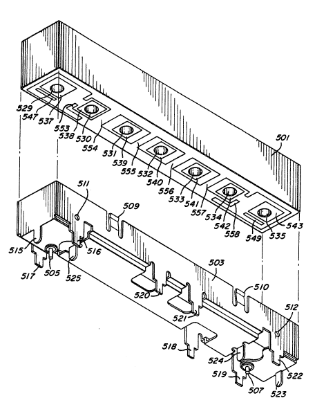
Re~erring now to Fig. 5, a dielectric filter
employing the present invention is shown in a exploded
perspective view. A block o~ dielectric material 501 is
placed in a carrying bracket 503 which per~ormq the
multiple functions of providing a rigid mounting platform
~uch that dielectric block 501 may be inserted into a
printed circuit board or other substrate, providing
~implified input and ou~put connections via ~eed through
terminals 505 and 507, and providing po~itive ground
contact between the conductiYe outer 6urface of
: dielec~ric block 501 and bracket 503 via contacts 509,
12~0(~30
- 7 -
510, 511, 512, and other contacts not shown. Contacts
509 and 510 additionally provide a dielectric block 501
locating function within the bracket 503. ~ounting
bracket 503 further provides mounting tabs 515-525 to
locate and ~upport the bracket and filter on a mounting
substratQ and provide positive ground contact for radio
frequency signals from the mounting bracket 503 to the
receiving mounting substrate. A mounting bracket for a
dielectric ~ilter has been disclosed in U.S. Patent ~Jo.
4,742,562 This previously disclosed bracket, however,
does not provide the simplified mounting of the bracket
of the present inventionO
In one preferred embodiment the dielectric filter
501 consists of a ceramic material and utilizes seven
internally plated holes as foreshortened resonators to
produce a band pass filter for operation in radio bands
reserved for cellular mobile telephone. In this
embodiment the conductive plating covering the ceramic
block 501 extends conformally on all surfaces except that
on which the resonator plating is wrapped from the holes
onto the outer surface. Thus, holes 529-535 have
corresponding plating 537-543 metalized on the outer
surface of block 501. These areas 537-543 are
electrically separate from the ground plating but provide
capacitive coupling to the ground plating. Additionally,
an input plated area 547 and an output plated area 549
provide capacitive coupling between the input terminal
505 and the coaxial resonator formed from the internally
plated hole 529 and its externally plated area 537 while
plated area 549 provides capacitive coupling between the
output terminal 507 and the output resonator formed from
plated hole 535 and external plated area 543. Ground
1~90030
stripes 553-558 are plated between the coaxial resonator
plated holes in order that inter-resonator coupling i~
adjusted.
Ceramic block 501 is inserted into bracket 503 with
the externally plated resonator areas 537-543 oriented
downward into the bracket 503 ~uch that addit~onal
shielding i~ a~orded by the bracket 503. Input mounting
pin 505 is connected to plated ar~a 547 and outpu~
1~ termlnal 507 is connected to plated area 549 as shown in
Fig. 6. Input terminal 50~, which may be a low shunt
capasity fee~ through such as a lOOB0047 ter~inal
manu~actured by ~irpax Electronics Inc., consits of a
solderable eyelet 601 and insulating glass bead 603
supporting a center conductor 605. The eyelet 601 is
conductively bonded to bracket 503 to provide a secure
mounting for the input connector 505. The center
conductor 605 is brought into contact with plated area
547 by the dimensions of the bracket 503 and the block
501. The center conductor 605 is soldered or otherwise
conductively bonded at one end to area 547 to provide a
reliable RF connection to plated area 547. The othPr end
; of the center conductor 605 may then be easily soldered
or plugged into a substrate which holds the mounting
bracket 503. A similar construction is employed for
output terminal 507 and its associated plated area 549.
A detail of the ~ounting bracket 503 is shown in
Fig. 7. The spacing of the mounting tabs 515 525 is
shown in detail for the preferred embodiment. ThesP
spacings are important a~ the frequencies of operation o~
this filter in order to maintain maximum ultimate
attenuation. Low ground path inductance in ths mounting
bracket is realized by placing mounting tabs 517 and 519
close to the input and output ports ~505 and 507 of Fig.
5 respectively) and the remainder o~ the tabs above the
~ide and bottom of the bracket 503. Connection between
the dielectri¢ block 501 and bracket 503 is assured near
~.Z9~03~
g
~he input and output terminals by contacts similar to
contacts 511 and 512 located close to the terminals. All
contacts, 509, 510, 511, and 512 (and the equivalent
contacts on the opposite side of the brackets not shown),
may be ~oldered or otherwise bonded to the dielectric
bloak 501 such that electrical connectlon may be
permanently assured.
It can be readily ascertained that the position of
the tabs 518, 520, and 521 are asymmetrical. Also, the
input/output terminal~ 505 and 507 are off~t from the
centerline o~ the brarket 503. This asymmetry enables a
"keying" of the bracket 503 so that a ~ilter can be
inserted in a printed circuit board or other substrate in
only one orientation.
one unique aspect o~ the present invention is shown
in Fig. 8. A dielectric filter block su~h as block 501
is mounted in bracket 503 and becomes a unitized circuit
component which may be inserted into a printed circuit
board or substrate 801. Appropriate holes 803 and 805
are located on the printed circuit board 801 to accept
the input and ou~put terminals 505 and 507 (not shown in
Fig.8), respectively. Further, appropriately located
slots ~15-825 are located in the printed circuit board
801 to accept the corresponding tabs of the bracket 503.
Thus the ~ilter 501 and bracke~ 503 may be mounted on a
circuit board aO1 lik any other component and circuit
runn~r~ may extend from the input hole 803 and the output
hole 805 such tha~ the filter may be electrically
connected to other circuitry with a minimum of effort.
The circuit board runners, 807 and 809, may be
constructed as stripline or microstrip trans~ission lines
to yield improved duplexer performance.
: Referring to Fig. 9, there is illustrated an
equivalent circuit diagram for the dielectric filter 501
utilized as a band pass filter. An inpu~ signal from a
signal ,ourc~ may be applied via terminal 505 to input
~29~33V
-- 10 --
ele.ctrode 547 in Fig. 5, whioh corresponds to the common
junction of capacitors 924 and 944 in Fig. 9. Capacitor
944 is the capacitance between electrode 547 and the
~urrounding ground plating, and capacitor 924 ls the
capacitance between electrode 547 and the coaxial
resonator provided by plated hole 529 in Fiy. 5. The
coaxial resonators provided by plated 529-535 in Fig. 5
correspond to shorted transmission lines 929-935 in Fig.
9~ Capacitors 937-943 in Fig. 9 represont the
capacitance between the coaxial r~eonators provided by
the extended plating 537-543 o~ ~he plated holes in Fig.
5 and the ~urrounding ground plating on th~ top sur~ac~.
Capacitor 925 repre~nts the capacitanca between the
reaonator provided by plated hole 53S and ~lectrode 549
in Fig. 5, and capacitor 945 represents the capacitance
between electrode 549 and the surrounding ground plating.
~n output signal is provided at the junction of
capacitors g25 and 945, and coupled to output terminal
547 for utilization by external circuitry.
Referring now to Fig. 10, there is illustra~ed a
multi-band filter comprised of two intercoupled
dielectric band pass ~ilters 1004 and 1012 and employing
the present invention. Two or more of the inventive band
pass filters may be intercoupled on a printed cirruit
boaxd or subctrate to provide apparatus that combines
and/or ~requency sor~s two RF signals into and/or ~rom a
composite RF signal. In one application of the preferred
embodiment the present invention is employed in the
arrangement of Fig. 10 which couples a transmit signal
from an RF transmitter 1002 to an antenna 1008 and a
receive signal from antenna 1008 to an RF receiver 1014.
The arrangement in Fig. 10 can be advantageously utilized
in mobile, portable, and fixed station radios as an
antenna duplexer. The transmit signal from RF
~ransmit~er 1002 is coupled ~o filter 1004 by a
transmission line 1005, realized by the plated runner 807
~29()030
of Fig. ~ on the printed circuit board in the preferred
embodiment, and the filtered transmit ignal i coupled
via circuit bsard runner transmission line 1006 (runner
809 of Fig. ~) to antenna 1008. Filter 1004 is a ceramic
band pass filter of the present invention, such as the
fllter illustrated in Figs. 5 and 8. The pa~s band of
filt~r 1004 is ~entered about the frequency of the
transmit ~ignal from RF transmikter 1002, while at the
~ame time greatly attenuating the ~requency of the
rscei~ed ~ignal. In addition, the length of transmission
line 1006 is select~d to maximize its i~pedance at the
frequen~y of the received signal.
A received ~ignal from antenna 1008 in Fig. 10 is
coupled by transmission line 1010, also realized as a
pxin~ed circuit board runner, to filter 1012 and thence
via circuit board runner transmission line 1013 to RF
receiver 1014. Filter 1012, which also may be one of the
inventive band pass filters illustrated in Figs. 5 and 8,
has a pass band centered about the frequency of the
receive signal, while at the ~ame time greatly
attenuating the transmit signal. Similarly, the length of
transmission line 1010 is selected to maximize its
impedanc~ at the transmit ~ignal frequency for further
attenuating the transmit signal .
In the embodiment o~ the RF ~ignal duplexing
apparatuq of Fig 10, transmit signals having a frequency
range from 825 MHz to 851 ~Hz and xeceive signals having
a fre~uency range ~rom 870MHz to 896MHz are coupled to
the antenna of a mobile radio. The dielectric band pass
filterc 1004 and 1012 utilize a dielectric of ceramic and
are constructed in accordance with the present invention
a~ shown in Fig. 5. The filters 1004 and 1012 each havP
a length of 3.0 inch and a width of 0.45 inch. The
3 5 height is a primary determinant of the frequency of
operation and, in the preferred em~odiment, is .49 inch
in the transmit filt~r 1004 and 0l44 inch in the receive
~290030
- 12 -
filter 1012. Filter 1004 has an insertion loss of 2.5 dB
and attenuate receive signals by at least 50 dB. Filter
1012 has an insertion loss of 3.0 dB and attenuates
receive signals by at least 60 dB. An alternative
interconnection of the circuit board mountable dielectric
block filters is shown in Fig. 11.
It is sometimes desirable to utilize two
swit hable antennas for a receiver so that the antenna
receiving the best signal may be switchably coupled to
the receiver and provide the well-known antenna diversity
function. By not providing a transmission line coupling
directly between transmission lines 1006 and 1010 (at
point A) but by inserting an antenna switch llO1
selecting a shared transmit/receive antenna 1103 and a
receive only antenna 1105 between the antennas, the
separate transmit and receive filters 1004 and 1012 may
be coupled by 180 reflection coefficient transmission
lines 1107 and 1109 in a fashion to provide a diversity
receive function.
The filter operational characteristics may be
determined by the metalization pattern employed on the
surface of the dielectric block which is not fully
metalized. Dielectric filters such as described herein
are intrinsically coupled by inductance. That is, the
magnetic fields in the dielectric material govern the
coupling. The inductance may be changed, and even
overcome, by introducing capacitance between the
resonators. Referring again to Fig. 5, it can be seen
that a seven pole configuration is realized by serially
coupling the resonators created by the metalized holes
529-535 and surface plating 539-543. As shown, the
capacitive coupling b~tween the resonators is restricted
by the grounded strip electrodes 554-557. Capacitive
coupling by metalization gaps or additional metalization
30~3~
, .
- 12a -
islands has been shown in the aforementioned U.S. Patent
4,742,562. According to one novel aspect of the present
~90~30
- 13 -
invention, a controlled capacitive coupling may be
achieved by providing incomplete strip alectrodes running
on the surface of the dielectric block between two
resonatsrs. In the pref2rred embodiment, incomplete
strip elactrodes 553 and 558, b~tween input resonator
and output re~onator and the other resonators, provide a
controlled capacitive coupling to enable combined
inductiv~ and capacitive coupling between adjacent
resonators. In practice, the use o~ inductiYe or
capaci~ive coupling provides ste~per ~ er attenuation
skirts on either the high side of the filter passband or
the low side of the filter passband, respectively.
When the dielectric filter blocks are csmbined as a
duplexer filter as shown diagra~matically in Fig. 10, it
is advantageous to employ a filter having a ~tep
att~nuation skirt above the passband as the filter
pa~sing the lower frequencies. ~l~o it is advantageous
to employ a filter having a steep attenuation skirt below
the passband as the filter passing the higher
frequencies. In this way, additional protection of
transmit and receive paths from each other can he
realized without additional filter resonator elements.
An advantage of the dielectric filter blocks of the
present invention is that the number and spacing of
resonators used in the transmitter filter 1004 (of Fig.
10) may be equal to the number and spacing of the
resonators in the receive ~ er 1012. The type o~
coupling is determined ~y the metalization pattern
employed. The transmit ~ilter 1004 utilizes inductive
coupling b~tween resonators as illus~rated in the
metalization pattern of Fig. 12A. The capacitive
coupling between the middle resonators is reduced by the
complete strip electrodes while the input and output
resonators utilize more capaci~ance in the incomplete
strip electrodes in their coupling to the middle
resonators. The receive filter 1012 utilizes capacitive
~29~030
- 14 -
coupling between resonators as illustrated in the
metalization pattern of Fig. 12B. Capacitive coupling is
enabled by the unblocked metalized resonators.
~Capacitive coupling may be enhanced by metalization
islands such as shown in the inductively coupl~d filter
of Fig. 12C).
A novel feature of the present invention creates
the ability of the coupling to be changed by changing the
metalization. Additionally, the mode of resonator
operation may be changed from band pass to band stop by
utilizing on~ or more resonators as a transmission zero
rather than as a transmission pole. Transmission zero
realization by metalization change only is shown in Fig.
12D. The output electrode 1203 is coupled to the first
transmission pole resonator 1205 by metalization runner
1207. Coupling is also realized from output electrode
1203 to transmission zero resonator 1209. In the
embodiment shown, the transmission zero is tuned to the
low side of the passband to realize additional rejection
on the low side of the passband. A filter utilizing
metalization such as that shown in Fig. 12D would be
suitable for use in a duplexer such as described above.
Additional zeros may be created by proper coupling
to other resonators. Such coupling is shown in the
metalization of Fig. 12E.
In summary, then, a printed circuit board
mountable, multiple resonator dielectric filter has been
shown and described. This filter utilizes metalized hole
resonators having coupling characteristics determined by
the metalization pattern on one surface of th~ dielectric
block. The dielectric block is metalized with a
conductive material on all but one surface from which the
hole resonators extend into the dielectric block.
12~30
- 14~ -
Electrode metalization around the holes provides
capacitive coupling to this conductive material and from
one resonator to an adjacent resonator. Capacitive
coupling between the resonators is controlled by an
-
~290030
- 15 -
electrode at least partially betwzen two adjacent hole
resonators to adjust the capacitive coupling between the
resonators. Input and output coupling is accomplished
via terminals asymmetrically arranged in a mounting
bracket. ~ounting tabs on the bracket opposite a
recessed area holding the dielectric block ~ecure the
filter to the circuit board and pro~ide ground
connection for the filter. Use o~ two ~iltera on a
printed circuit board with copper runners forming
transmission lines o~ approprlate el~ctrical length
creates a duplexer for tran~ceiver applications.
Therefore, while a particular embodiment of the invention
has been described and shown, i~ should be understood
that the in~ention is not limited thereto since many
modifications may be made by those skilled in the art.
It is therefore contemplated to cover any and all such
modifications that fall within the true spirit and scope
of the basic underlying principles disclosed and claimed
herein.
2~