Note : Les descriptions sont présentées dans la langue officielle dans laquelle elles ont été soumises.
~ 91~
WRITE CLOCK GENERATOR FOR TIME BASE CORRECTOR
BACRGROUND OF T~E INVENl'ION
Field of the Invention
The present invention relates generally to a
write clock generator incorporated in a time base
corrector for a video tape recorder and more
specifically to a write clock generator which can
generate a write clock signal having accurate phase
information and accurate frequency information on video
signals reproduced from a video tape.
Description of the Prior Art
In a time base corrector for a video tape
recorder, a synchronizing signal SYNC and a burst signal
BURST are separated from a video signal VDIN reproduced
from a tape. The write clock generator generates a
write clock signal WCK and a write start pulse signal
WZERO involving time base fluctuations (i.e. jitter) in
synchronism with the above separated signals SYNC and
BURST. The write start pulse signal WZER0 serves as a
head address designation signal for each scanning line
to a memory. Memory addresses are incremented in
sequence in response to the write clock signal WCK in
order to write the reproduced video signal VDIN in a
memory scanning line by scanning line. The video signal
stored once in the memory is read in response to a read
start pulse RZER0 and a read clock signal RCK generated
from a read clock generator in response to a stable
reference pulse signal VDREF. The read video signal is
outputted from the time base corrector as a reproduced
video signal VD0UT without including jitter together
with a synchronizing signal SYNCX, a burst signal BURSTX
and a blank pulse BLKX all applied from the read clock
generator.
In the time base corrector as described above,
in order to accurately write the reproduced video signal
~,9181~
~ 2 --
in the memory, it is necessary to generate a write clock
signal WCK the phase of which accurately varies
according to jitter included in the reproduced video
signal VDIN, because color off~et will be produced.
A write clock generator can accurately
generate a write clock signal WCK including phase
information and frequency fluctuation information on the
reproduced video signal VDIN. In this method, the write
clock signal WCK is generated in phase-synchronism with
the reproduced burst signal suRsT. Although the initial
phase information can be included, since it is impossible
to give frequency fluctuat;on information to the write
clock signal WCK, this method is not practical in the
case where the reproduced video signal includes
relatively great frequency fluctuations.
To overcome the above problem, there has been
proposed another method in which a write clock signal
WCK is generated on the basis of frequency fluctuation
information obtained from the reproduced horizontal
synchronizing signal SYNC and phase information obtained
from the reproduced burst signal BURST. In the write
clock generator of this method, the reproduced
horizontal synchronizing signal SYNC is applied to a
phase locked loop circuit to form a synchronizing signal
including frequency fluctuations involved in the
reproduced video signal VDIN, and the formed
synchronizing signal is phase-shifted so as to
synchronize with the phase of the reproduced burst
signal BURST. In this method, however, there exist such
shortcomings that the circuit is complicated, because
the frequency fluctuations are suppressed within + half
wave in digital fashion and further the synchronizing
circuit is configured in analog fashion.
S~MMARY OF T~E INVENTION
Wlth these problems in mind, therefore, it is
the primary object of the present invention to provide a
write clock generator for a time base corrector, which
can generate a write clock signal including accurate
phase information and accurate frequency fluctuation
information on a reproduced video signal, in spite of a
relatively simple circuit configuration.
To achieve the above-mentioned object, in a
write clock generator for a time base corrector for
generating a write clock signal to a time base
correcting memory on the basis of a burst signal and a
horizontal synchronizing signal both separated from a
reproduced video signal in order to reduce time base
fluctuations involved in the reproduced signal, the
write clock generator according to the present invention
comprises (a) means for generating a write clock signal
in response to a burst signal included in the reproduced
video signal, an initial phase of the write clock signal
being synchronized with a phase of the burst signal; ~b)
means for generating a frequency fluctuation signal in
response to a horizontal synchronizing signal included
in the reproduced video signal; (c) means for detecting
a difference in frequency between the write clock signal
and the frequency fluctuation signal and generating a
frequency difference signal; and ~d) means connected to
said write clock signal generating means, for
controlling a frequency of the write clock signal so
that the difference in frequency between the write clock
signal and the frequency fluctuation signal is reduced
to zero in response to the frequency difference signal.
The write clock signal generating means
comprises a start pulse generator and a start-stop VCO~
The frequency fluctuation signal generating means
comprises a PLL circuit~ The frequency difference
detecting means comprises a frequency discriminating
circuit including first and second switching circuits
and a frequency discriminator, first and second
- ~9~
holding circuits, and a differential voltage detector.
The VCO starts to oscillate in response to a
start pulse signal ST~T generated by the start pulse
generator in response to a reproduced burst signal BURST
and outputs a write clock signal WCK. Therefore, the
initial phase of the write clock signal WCK is in
synchronism with the reproduced burst signal BURST, that
is, with the phase of the reproduced video signal. The
frequency of the write clock signal WCR is detected by
the frequency discriminator in the form of an amplitude
of a voltage signal, and held by the first holding
circuit as a dc voltage signal.
On the other hand, the PLL circuit generates a
frequency fluctuation signal Sl9 in response to a
reproduced horizontal synchronizing signal H so as t'o
include time base fluctuations, and held by the second
holding circuit in the same way. The differential
voltage detector applies a dc control signal
representative of a difference in frequency between the
two signals WCK and Sl9 to the VCO so as to eliminate
the frequency difference. Therefore, the generated
write clock signal WCK includes accurate phase
information and accurate time base fluctuation
information on a reproduced video signal VDI~. Thus,
it is possible to obtain a video signal ~f good
reproducibility in spite of a relatively simple circuit
configuration.
BRIEF DESCRIPTION OF TDE DRAWINGS
The features and advantages of the write clock
generator for a time base corrector according to the
present invention will be more clearly appreciated from
the following description of the preferred embodiment of
the invention taken in conjunction with the accompanying
drawings in which:
Fig. l is a schematic block diagram showing
the whole circuit configuration of a time base corrector
~9~
in which the write clock generator according to the
present invention is to be incorporated;
Fig. 2 is a schematic block diagram showing a
first embodiment of the write clock generator according
to the present invention,
Fig. 3 is a diagram showing the frequency
characteristics of a frequency discriminator included in
the write clock generator according to the present
invention shown in Fig. 2;
Fig. 4 is a schematic block aiaqram showing a
second embodiment of the write clock generator according
to the present invention; and
Fig. 5 is a timing chart for assistance in
explaining the function of a frequency divider in~l~ded
in the write clock generator shown in Fig. 4.
DETAILED DESCRIPTION OF T~E PREFERRED EMBODIMENTS
. . . _ _ _
To facilitate an understanding of the present
invention, a brief reference will be made to a time base
corrector used for a video tape recorder, to which the
write clock generator according to the present invention
is applied.
With reference to Fig. 1, a video signal VDIN
is reproduced from a tape. ~ reproduced synchronizing
signal SYNC and a reproduced burst signal BURST are
separated ~rom a reproduced video signal VDIN through a
synchronizing and ~urst signal separator 1. The two
separated signals SYNC and BURST are applied to a write
clock generator 2.
The write clock generator 2 generates a write
clock signal WCK and a read start pulse signal WZERO in
synchronism with a reproduced synchronizing signal SYNC
and a reproduced ~urst signal BURST both having
fluctuations on a time ~ase. The write clook signal WCK
is given to an analog-digital converter 3 as a sampling
pulse signal and also to a memory controller 4 together
with tne write start pulse signal WZERO.
-- 6 --
In response to the write start pulse signal
WZERO, the memory controller 4 designates each head
address of each scanning line to a memory 5 and
thereafter writes video signal data VDIND obtained from
an analog-to-digital converter 3 for each scanning line
(i.e. for each lH) in the memory 5 in sequence by
sequentially incrementing the address in response to the
write clock signal WCK.
The data written in the memory 5 are read in
response to a read clock signal RCK -and a read start
pulse signal RZERO generated from a read clock generator
6 on the basis of a reference pulse signal VDREF having
a stable period.
The video signal data are converted into
anaLog signals through a digital-to-analog converter 7
driven in response to the read clock signal RCK and then
applied to a phase adjuster 8. The phase adjuster 8
generates a reproduced video output signal VDOUT
together with a synchronizing signal SYNCX, a burst
signal BURSTX, and a blank pulse BLKX all given from the
read clock generator 6.
In the time base corrector as shown in Fig. 1,
when video signal data are written in the memory 5 for
each scanning line, if an accurate write clock signal
WCK, the phase of which accurately varies according to
jitter included in the reproduced video signal VDIN, is
not generated, it is impossible to correctly write the
reproduced video signal in the memory 5. That is to
say, it is impossible to obtain reproduced video output
signals VDOUT of good reproducibility, because color
offset wil:L be produced.
In view of the above description, reference is
now made to a first embodiment of the write clock
generator for a time base corrector according to the
present invention.
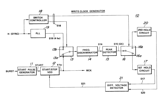
With reference to Fig. 2, a first embodiment
-- 7 --
of the present invention will be described. In the
drawing, the reference numeral 10 denotes a write clock
generator to be incorporated in the time base corrector
shown in Fig. 1.
In the write clock generator 10, the
reproduced burst signal BURST separated through the
synchronizing burst separator 1 (shown in Fig. 1) is
given to a start pulse generator 11. The start pulse
generator 11 extracts a desired wave of the burst signal
BURST on the basis of the zero-cross point of the
reproduced burst signal BURST, and gives the wave signal
STRT to a start/stop type voltage controlled oscillator
(VC0) 12 after waveform shaping.
The start/stop type VC0 12 is reset when the
start pulse signal STRT is given, and oscillates with
the phase being shifted to a reference phase
compulsorily. Further, the frequency of the VC0 12 can
be controlled on the basis of a voltage applied thereto.
Since the frequency is selected to a frequency 4fsc four
times higher than the subcarrier frequency fsc, this
oscillation signal is outputted as a write clock signal
WCK. Further, the write clock signal WCK is given to a
frequency discriminator 14 through a first switching
circuit 13.
The frequency discriminator 14 is composed of
a low-pass filter, for instance. As shown in Fig. 3,
the frequency characteristics are such that the
frequency 4fsc four times higher than the subcarrier
frequency is located roughly at a center of the
frequency discrimination range AF (cut-off frequency
range), and the frequency band BF within which the
frequency 4fsc can fluctuate according to the time base
fluctuations of the reproduced video signal VDIN is
located within this frequency discrimination range AF.
Therefore, it is possible to obtain a discrimination
signal S14 the amplitude of which varies according to
-- 8 --
the frequency of the write clock signal WCK through this
frequency diseriminator 14.
A peak detector 15 holds the peak voltage of
the discrimination signal S14 supplied from the
frequency discriminator 14 and rectifies it into a dc
voltage, and the de voltage signal S15 is given to and
held by a first holding circuit 17 through a second
switehing circuit 16.
Here, sinee the first switching circuit 13 and
o the second switching circuit 16 are switched in linkage
with each other, when the first switching eircuit 13 is
switehed to a first input terminal 13a to which the
write eloek signal WCK is given, the seeond switehing
eireuit 16 is switehed to a first output terminal 16a
eonneeted to the first holding eireuit 17. Therefore,
the holding eireuit 17 holds the de voltage signal S15
representative of the frequeney of the write eloek
signal WCK.
Further, in the write eloek generator 10, the
reprodueed horizontal synehronizing signal H of the
reprodueed synehronizing signal SYNC separated through
the synehronizing burst separator 1 (shown in Fig. 1) is
given to a PLL (phase locked loop) eireuit 19. The PLL
eireuit 19 generates a frequeney fluetuation signal Sl9
whieh fluetuates with a frequeney 4fse four times higher
than the subearrier frequeney fse as its eenter and
gives the signal Sl9 to the seeond input terminal 13b of
the first switehing eireuit 13, the signal Sl9 being
obtained by multiplying the horizontal synchronizing
signal H so as to inelude the time base fluetuations as
they are.
A seeond holding eireuit 20 holds the de
voltage signal S15 of the peak deteetor 15 when the
first switehing eireuit 13 is eonneeted to the seeond
input terminal 13b and the seeond switehing eireuit 16
is eonneeted to the seeond output terminal 16b in
91~
linkage with the first switching circuit 13. Therefore,
the holding circuit 20 holds the dc voltage signal S15
according to the frequency of the frequency fluctuation
signal Sl9.
The two held output signals S17 and S20 of the
first and second holding circuits 17 and 20 are given to
a differential voltage detector 21, respectively and
subtracted by the differential voltage detector 21. The
difference voltage signal S21 obtained by the
subtraction is given to the start/stop-type VCO 12 as a
control signal. In response to this control signal S21
the VCO 12 is controlled and oscillates in such a way
that the difference voltage signal S21 becomes zero in
voltage. Therefore, the write clock signal WCK includes
frequency fluctuations of the frequency fluctuation
signal Sl9.
Here, the switching circuits 13 and 16 are
controllably switched by a switching controller 18. A
reproduced horizontal synchronizing signal H is given to
the switching controller 18, and the controller 18 forms
a switching control signal S18 the logical level of
which is reversed for each horizontal synchronization
time interval, for instance, on the basis of the
reproduced horizontal synchronizing signal H in order to
switch the switching circuits 13 and 16 for each
horizontal synchronization time interval.
In the circuit configuration shown in Fig. 2,
since the start/stop type VCO 12 is reset for each
horizontal synchronization time interval in response to
the start pulse signal STRT formed by the start pulse
generator 11 in response to the reproduced burst signal
BURST, the initial phase of the write clock signal WCK
matches the phase of the reproduced video signal VDIN.
Further, the frequency of the write clock
signal WCK is converted into a dc voltage signal S15 by
the write clock signal frequency controlling means
~L?,9iL~
-- 10 --
composed of the first switching circuit 13, the
frequency discriminator 14, the peak detector 15, and
the second switching circuit 16, and is held by the
first holding circuit 17. In contrast with this, the
- 5 frequency fluctuation signal Sl9 formed on the basis of
the reproduced horizontal synchronizing signal ~ is
converted into a dc voltage signal 16 by khe write clock
signal frequency controlling means composed of the first
-~ switching circuit 13, the frequency discriminator 14,
;~ lO the peak detector 15, and the second switching circuit
16, and is held~by the second holding circuit 20.
These held voltage signals S17 and S20 are
subtracted by the differential voltage detector 21. The
difference voltage signal S21 is applied to the VCO 12
to control the oscillation frequency of the VCo 12 so
that the difference voltage becomes zero. As described
above, the wrlte clock signal WCK involves the time base
fluctuations of the frequency fIuctuation signal Sl9,
that is, the time base fluctuations of the reproduced
video signal VDIN.
As described above, according to the circuit
;~ ~ shown in Fig. 2, i~ is possible to obtain a ~rite clock
signal WCK having the initial phase information given by
the reproducèd burst slgnal BURST and the frequency
7~ fluctuation information given by the reproduced
; horizontal synchronizing signal H. Therefore, the phase
information on the reproduced video signal VDIN is
detected by using the oscillation output of the VCO 12
~ oscillating on the basis of the reproduced burst signal
; 30 BURST as the write clock signal WCK, and the frequency
fluctuation information on the reproduced video signal
VDIN is detected by allowing the frequency of the write
clock signal WCK to be fluctuated on the basis of the
frequency fluctuation signaI Sl9. Since the circuit is
3~ configured as described above, it is possible to
- simplify the circuit configuration without use of the
:
~?~9~
- 11 -
conventional complicated phase synchronizing circuit
which compulsorily implements the phase synchronization
after the frequency fluctuation information has been
detected.
Further, since the route through which the
frequency is detected is common to the write clock
signal and the frequency fluctuation signal, an error
due to temperature difference in the route being not
generated, it is possible to detect the frequency
difference precisely.
In operation, the VCO 12 starts to oscillate
on the basis of the start pulse signal STRT formed by
the start pulse generator 11 on the basis of one wave of
the reproduced burst signal BURST, and the oscillation
~5 output is generated as the write clock signal WCK.
Therefore, the initial phase of the write clock signal
WCK is in synchronizm with the phase of the reproduced
burst signal BURST, that is, the reproduced video signal
VDIN.
Further, the frequency of the write clock
signal WCK is detected in the form of amplitude
fluctuation by the frequency discriminator 14 and
further converted into a dc voltage signal through the
peak detector 15, being held by the holding circuit 17.
On the other hand, a dc voltage signal varying according
to the frequency of the frequency fluctuation signal Sl9
is held in the same way. The signal Sl9 is formed by
the PLL circuit 19 so as to have the time base
fluctuations of the reproduced video signal VDIN on the
basis of the reproduced horizontal synchronizing signal
H.
Therefore, since a control signal S21 is given
from the differential voltage detector 21 to the VCO 12
to reduce the difference between these two held dc
voltage signals S17 and S20, the write clock signal WCK
is to follow up the time base fluctuations of the
reproduced video signal VDIN.
~9~
- 12 -
As a result, the write clock signal WCK
accurately includes the phase information and the time
base fluctuation information on the reproduced video
signal VDIN. Therefore, when the video signal is
written in the memory 5 in response to thi~ write clock
signal WCK, it is possible to obtain a picture having a
good reproducibility. On the other hand, the circuit
configuration is markedly simplified as compared with
the conventional one.
o In addition, since the write- clock signal WCK
and the frequency fluctuation signal Sl9 are F-V
converted through the same route, it is possible to
effectively c`ancel signal level fluctuations due to
temperature change in both the signals WCK and Sl9.
Fig. 4 shows a second embodiment of the
present invention, which includes a circuit element for
preventing the state where the frequency difference
signal S21 cannot be detected accurately because the
duty factor is different between the write clock signal
WCK and the frequency fluctuation signal Sl9.
For instance, in the case where the duty
factor of the write clock signal WCK is 50~ and that of
the frequency fluctuation signal Sl9 is 30%, as depicted
in Figs. 5~A) and ~C), even if the frequencies of both
the signals WCK and Sl9 are the same, the amplitude AWcK
of the fundamental harmonic component fwcK of the write
clock signal WCK is greater than that Asl9 of the
fundamental harmonic component fSl9 of the frequency
fluctuation signal Sl9 after Fourier transformation. As
a result, when ~he write clock signal WCK and the
frequency fluctuation signal Sl9 having a different duty
factor, respectively are passed through the frequency
discriminator 14 shown in Fig. 2, since the amplitudes
of tne inputted fundamental harmonic components are
different from each other, the output signal S14 has
different amplitudes in spite of the fact that the
~9~
- 13 -
frequency is the same. Thus, the oscillation of the
start/stop type VCo 12 being controlled erroneously.
To overcome the above problem, in the
embodiment shown in Fig. 4, a 1/2 divider 25 is further
disposed between the first switching circuit 13 and the
frequency discriminator 14 to always keep the duty
factor of the signal S25 at 50%, for instance.
Therefore, the write clock signal WCK having a duty
factor 50% as shown in Fig. 5(A) is divided into a
signal S250 having a duty factor 50% -as shown in Fig.
5(B), and the frequency fluctuation signal Sl9 having a
duty factor 30% as shown in Fig. 5(C) is divided into a
signal S25, having a duty factor 50% as shown in Fig.
5(D).
According to the second embodiment shown in
Fig. 4, even when the duty factor is different between
the frequency fluctuation signal Sl9 and the write clock
signal WCK, it is possible to accurately detect the
difference in frequency between the two signals Sl9 and
WCK, and therefore it is possible to permit the write
clock signal WCK to follow up the frequency fluctuations
of the reproduced video signal VDIN.
In the above-mentioned embodiment, the
frequency discriminator 14 composed of low-pass filters
has been explained; however, without being limited to
this, it is possible to use a band-pass filter, a
high-pass filter, etc. In summary, it is possible to
adopt such frequèncy characteristics that the frequency
of the fundamental harmonics of the coming signals (WCK,
3~ Sl9, divided signals thereof) lies within a cut-off
frequency range ~f the filter. In these cases, it is
possible to obtain the effect similar to the
above-mentioned embodiments.
Further, in the above embodiments, the
low-pass filter 14 and the peak detector 15 are used in
common with the frequency fluctuation signal Sl9 and the
- 14 -
write clock signal WCK. Howe~er, it is also possible to
separate these sections independently. In this case,
the switching element can be omitted.
As described above, in the write clock
generator according to the present invention, the
oscillation output signal of the VCo oscillating on the
basis of the reproduced burst signal is outputted as the
write clock signal; the frequency fluctuation signal
following the time base fluctuations of the reproduced
video signal is formed on the basis Qf the reproduced
horizontal synchronizing signal; and the VCO is
controlled according to the difference in frequency
between the frequency fluctuation signal and the write
clock signal. Therefore, it is possible to realize the
write clock generator for a time base corrector of
simple circuit configuration which can generate the
write clock signal having accurate phase information and
accurate frequency fluctuation information upon the
reproduced video signal. Additionally,- since the write
clock signal and the frequency fluctuation signal are
F-V converted through the same circuit elements, it is
possible to cancel the signal fluctuations caused by
temperature fluctuations, for instance.