Note : Les descriptions sont présentées dans la langue officielle dans laquelle elles ont été soumises.
-1- RCA 83,778
DIRECT DC TO RF CONVERSION BY IMPULSE EXCITATION
Backqround of the Invention
The present invention relates to converting
DC (direct current) to RF (radio frequency), and more
particularly, using a monolithic optical switch to impulse
excite a monolithic resonator.
It is known to use an optical switch coupled
to a DC supply in order to inexpensively generate high
power microwave and millimeter wave signals. Indeed,
above about 200GHz such an arrangement is probably the
only practical way of generating signals, except possibly
for mixing the signals from two lasers together and
selecting the difference frequency signal, since about
200GHz is the limit for conventional oscillators. In
particular, such an arrangement provides such high
sub-millimeter wave signals due to the very fast
switching time, e.g., one picosecond or less, of the
optical switch, which results in harmonics in the
sub-millimeter range.
Such arrangements are shown in the articles
"High-Frequency Waveform Generation Using Opt~electronic
Switching in Silicon" by M. M. Proud, Jr. and S. L. Norman,
I.E.E.E. Trans. Microwave Theory Tech., MTT-26, pp. 137-140,
1978, and "Direct DC to RF Conversion by Picosecond
Optoelectronic Switching", by C. S. Chang et al., IEEE
MTT-S International Microwave Symposium Digest, 1984,
pp. 540-541, wherein the optical switch comprises bulk
silicon and the later article shows a resonator comprising
a cavity, which is bulky. ~Further, the bulk silicon or
other semiconductor must have a high OFF resistance in
order to withstand the applied high DC voltage. However,
it is then difficult to make a good ohmic con~act to
the bulk silicon resulting in a high ON resistance, and
therefore low efficiency and eventual burn out of the
switch due to the heat dissipation thereof. One can make
such an arrangement in monolithic form to reduce the size
thereof, but the other above-mentioned problems remain.
`~k
~q~z~z~z
-2- RCA 83,77
Further, it is normally desirable to have a plurality
of such arrangements in monolithic form in order to,
e.g., form a phased array. It has been found that using a
bulk semiconductor optical switch causes unwanted coupling
between the DC to RF converters and interference to the
optically triggered timing thereof.
It is, therefore, desirable to have a DC to RF
converter that is efficient, reliable, and a plurality
of which can be made in monolithic form without undesired
coupling therebetween.
Summary of the Invention
-
A device for converting voltage from a DC supply
to RF comprises a monolithic resonator, and a monolithic
lateral PIN diode optical switch means having a pair of
opposite conductivity type regions adapted to be coupled
to the DC supply, one of said regions coupled to said
resonator, and an intrinsic region adapted to receive
an optical switching signal.
Brief Description of the Drawings
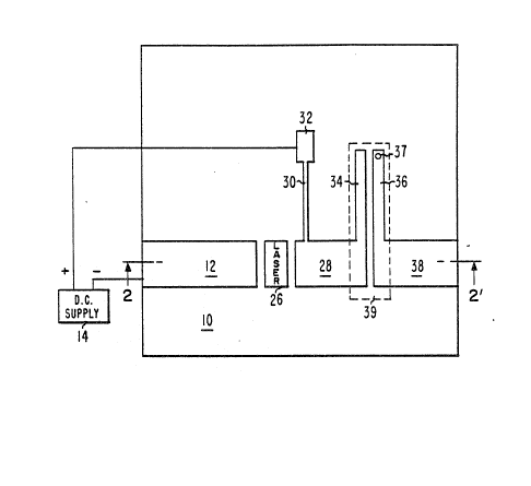
FIGURE 1 is a top view of the invention; and
FIGURES 2A and 2B are cross-sectional views
taken along the line 2-2' of FIGURE 1 of first and second
embodiments of the invention, respectively.
Detailed Description of the Preferred Embodiments
As shown in FIGURES 1 and 2A, the first embodiment
comprises an intrinsic substrate 10 overlying a ground
plane conductor 11 and having thereon a first conductor 12.
The conductor 12 has one end coupled to the negative termlnal
of a D.C. supply 14 of up to about 1000 volts and capable
.
, : .
.
-
-3- RCA 83,778
of providing, e.g., 20 amperes and another end coupled to
a P+ conductivity type electrode region 16 of a monolithic
lateral PIN diode 18. The diode 18 additionally comprises
an intrinsic (I) conductivity type region 20 adjacent
S the region 16, an N+ conductivity type electrode region 22
adjacent the region 20, and an insulating layer 24 overlying
the I region 20 and portions of the electrode regions 16
and 22. A laser 26 is disposed over the I-region 20 for
illumination thereof. Obviously, the laser 26 could be
remotely disposed and optically coupled to the I-region 20
by means of an optical fiber (not shown) if so desired.
A second conductor 28 overlies the substrate 10
and has one end coupled to the region 22. The conductor 28
has an extension 30 that is electrically one quarter
wavelength long at the frequency of interest in order to
act as a radio frequency choke. A terminal pad 32 lies at
the end of the extension 30 and is coupled to the positive
terminal of the supply 14. It will be appreciated that
the diode 18 is thereby reversed biased. A bar 34 extends
parallel to and spaced from a bar 36 of a third conductor
38. Optionally, a conducting via hole 37 is disposed at
the end of the bar 36 to connect it to the ground plane 11.
The conductors 12, 28 and 38, including the extensions 34
and 36, form microstrip transmission lines with the ground
plane 11 having a characteristic impedance of 50 ohms.
The bars 34 and 36 also comprise a monolithic resonator
and impedance transformer 39 having an electrical length
between about one-eighth to one-quarter wavelength at
the frequency of interest. The transformer converts
the impedance of the diode 18, to 50 ohms to match the
characteristic impedance of the microstrip conductor 38.
Such transformers are disclosed in the article
"Silicon Avalanche-Diode Microstrip L-Band Oscillator,"
by A. Rosen et al., I.E.E.E. Trans. on Microwave Theory
and Techniques, Vol. MTT-18, pp. 979-981. Briefly, the
bars 34 and 36 act as coupled TEM mode transmission lines.
Their width is about 89~m (micrometer) and their inner
edge-to-inner edge spacing is 25~m for a selected
-4- RCA 83,778
frequency of 6GHz. The via hole 37 causes the resonator 39
to provide an impedance match over a broader bandwidth.
The outpu~ signal is provided at the right hand end of the
conductor 38, which can be fitted with a type OSM connector
(not shown) or the conductor 38 can just be extended to
combine with other devices in accordance with the invention
to obtain greater power output.
The conductors or conducting layers 11, 12, 28
and 38 including elements 30, 32, 34 and 36, can comprise
a compound layer of a Cr layer with a thickness between
about 400-1000 Angstroms and a Au layer with a thickness
of about l~m with the Cr layer next to the substrate 10.
The substrate 10 has a thickness of about 6 to 7 mils
(152 to 177~m) and can comprise any semiconductor, e.g., -
Si or Ge, or group III-V semi-insulator, e.g., GaAs, InP,
but Si is preferred since it has a long carrier lifetime,
. thereby minimizing the duty cycle, and thus, the heating
of the laser 26. The insulating layer 24 can comprise any
insulator such as sio2 or Si3N4. The regions 16 and 22 can
be doped with B and P, respectively, with a doping level of
about 1019 cm 3. As known in the art, the I-region 20 is
actually a weakly doped P or N conductivity type region
since it is very difficult to obtain a region that is
exactly intrinsic. It is preferred to use a weakly doped
N-conductivity for the region 20 with a doping level
between about 1O12 to 1014 cm 3 and a resistivity of about
4000 ohm-cm since a weakly doped P-conductivity type region
can change to a weakly doped N-conductivity type at high
temperatures, thereby changing the electrical characteristics
of the diode 18. The laser 24 must provide light having
a minimum frequency depending upon the material of the
substrate 10 in order to have enough energy to generate
photocarriers so that the ON resistance of the diode 18
is low for maximum efficiency. With a substrate 10 of
Si, a CW mode locked Nd:YAG laser frequency dot~led to
provide green light of 532nm (nanometers) wavelength was
satisfactory. In particular, such a laser has picosecond
rise times so that millimeter wave harmonics are generated.
_5_ RCA 83,778
In operation, the laser 26 is initially OFF,
and thus the reversed biased diode 18 is also OFF
(non-conducting). When the laser 26 is turned ON, the
light that is emitted generates photocarriers in the
I-region 20, thereby turning ON the diode 18. Current
is then drawn from the source 14, which has a high
harmonic content due to the steepness of the light pulse.
The desired harmonic is then selected by the monolithic
resonator 39 and also impedance transformed thereby.
The laser 26 is then turned OFF. Thereafter the cycle
is repeated. It has been found that a cycle period of
about 10ns (nanoseconds) provides a nearly CW output
signal for a substrate 10 of Si. An efficiency of
about 1% was obtained.
lS It will be appreciated that the use of the PIN
diode 18, which is reversed biased when OFF, instead of
.~ bulk Si as the optical switch, prevents currents from
flowing in the substrate 10 between a plurality of DC to
RF converters as described above and affecting their timing.
A possible problem with the above described
embodiment is that the OFF resistance of the Si substrate 10
may not be high enough to obtain a desired high Q for the
resonator 39. One can use GaAs for the substrate 10 to
obtain a high value of Q due to its high OFF resistance, but
since GaAs has a shorter carrier lifetime than Si, a higher
pulse repetition rate is then required of the laser 26,
which might result in excessive heat dissipation thereof~
FIGURE 2B shows a second embodiment for
obtaining the best characteristics of both materials,
wherein corresponding elements have corresponding reference
numerals. This embodiment features a semi-insulating
layer 40 of about 3~m thickness, made of, e.g., a group
III-V material such as GaAs, InP, etc., which can be
deposited on the substrate 10 by molecular beam epitaxy
or metalorganic chemical vapor deposition as disclosed
in the article "Organometallic Chemical Vapor Deposition
of GaAs and AlGaAs for Microwave Applications, R. J. Menna
et al., RCA Review, December 1986, Vol. 47, No. 4,
s~
-
~6- RCA 83,778
pp. S78-617. The layer 40 acts as the substrate for the
conductors 12, 28, and 38, and therefore, the resonator 39.
The diode 18 is still preferrably fabricated in a Si
substrate 10. First and second conducting bridges 42 and
44 such as Ag, Al, Cu, etc., preferrably Au, connect the
layer 12 to the region 16 and connect the layer 28 to
the region 22, respectively. First and second insulating
filets 46 and 48 (such as a polyimide or an oxide) are
disposed underneath the bridges 42 and 44, respectively,
and overlie the substrate 10 and prevent the bridges from
contacting the intrinsic portions of the substrate 10. The
filets 46 and 48 can be eliminated and the bridges 42 and 44
can then be air bridges. If the doped regions 16 and 22
are near the edges of the Iayer 40, then a continuation of
the layers 12 and 28 to these regions, respectively, can be
used as the bridges 42 and 44 without the filets 46 and 48.
It will be appreciated that since GaAs has a
lower dielectric loss than Si, the microstrip transmission
lines formed by the conductors 12, 28, and 38, including
the resonator 39, have a higher Q than the embodiment of
FIGURE 1 while the diode 18 has as long a carrier lifetime
as the embodiment of FIGURE 1 since the substrate 10 is
still si.
The embodiment of FIGURE 2B has a calculated
efficiency of about 10%.
.
.