Note : Les descriptions sont présentées dans la langue officielle dans laquelle elles ont été soumises.
~:9303~
SAMPLE HOLDING CIRCUIT
BACRGROUND OF T~E INVENTION
This invention relates to a sample holding
circuit operable as an output circuit for charge coupled
devices or other delay line.
Charge coupled devices or other delay line
require sample holding circuits. In such conventional
sample holding circuits however, a serious problem
occurs in that the signal DC level shifts with respect
to the power source or ground potential. This leads to
the requirement for complicated circuit designs and an
inability to widen dynamic range and operation margin of
the circuit. In addition, the conventional sample
holding circuit cannot operate reliably on a low voltage
and incompatible with the recent tendency toward power
source size reduction. Thus, there has been a demand
for a practical approach which solves the problems
associated with DC level shift introduction.
20 SUMMARY OF THE INVENTION
It is a main object of the invention to
provide an improved sample holding circuit which can
operate without causing any DC level shift.
Another object of the invention is to provide
an improved sample holding circuit which can operate
reliably on a low voltage.
There is provided, in accordance with the
invention, a sample holding circuit comprising a signal
source for generating a series of timing pulses, and a
sample holding stage having an input for receipt of a
voltage signal. The sample holding stage includes a
capacitor and a switching transistor responsive to each
of the timing pulses for communicating the voltage
signal to charge the capacitor. The sample holding
stage has an output for producing a signal corresponding
to the voltage stored in the capacitor. The sample
3~
1~93G31
holding circuit also comprises at least one amplifier
circuit associated with the sample holding stage. The
amplifier circuit is operable to amplify an input signal
at a gain substantially equal to 1 without introducing
any DC level shift.
BRIEF DESCRIPTION OF T~E DRAWINGS
This invention will be described in greater
detail by reference to the following description taken
in connection with the accompanying drawings, in which:
Fig. 1 is a schematic block diagram showing
one embodiment of a sample holding circuit made in
accordance with the invention;
Fig. 2 is a diagram of an analog signal
coupled to the input terminal of the sample holding
circuit;
Fig. 3 is a diagram of the signal generated at
the output terminal of the sample holding circuit;
Fig. 4 is a circuit diagram showing the
amplifier circuit of Fig. l;
Fig. 5 is a circuit diagram showing another
form of the amplifier circuit;
Fig. 6 is a circuit diagram showing a prior
art sample holding circuit; and
Fig. 7 is a circuit diagram showing another
form of the prior art sample holding circuits.
DETAILED DESCRIPTION OF TDE INVENTION
-
Prior to the description of the preferred
embodiment of the invention, the prior art sample
holding circuits of Figs. 6 and 7 are briefly described
in order to specifically point out the difficulties
attendant thereon.
Referring to Fig. 6, the prior art sample
holding circuit includes a sample holding stage
including a capacitor 62 and a switching transistor 61
operable to communicate a signal to charge the capacitor
62 at appropriate sampling times. The sample holding
~93~3~
stage is connected on its input side to an inverter
circuit including a pair of MOS transistors 63 and 64
and on its output side to an inverter circuit including
a pair of M0S transistors 65 and 66. With such a
circuit arrangement, however, a DC level shift is
introduced between the transistors 64 and 61 and an
additional DC level shift is introduced between the
transistors 61 and 65. In addition, gain changes would
occur within the circuit.
Referring to Fig. 7, the prior art sample
holding circuit includes a sample holding stage
including a capacitor 72 and a switching transistor 72
operable to communicate a signal to charge the capacitor
72 at appropriate sampling times. The sample holding
stage is connected on its input side to a pair of NMOS
transistors 73 and 74 to provide source-follower
operation and on its output side to a pair of NMOS
transistors 75 and 76 to provide source-follower
operation. With such a circuit arrangement, however, a
DC level shift is introduced in the MOS transistors 73
and 75. In addition, each of the NMOS transistor pairs
have a gain in the order of 0.9 so that the total gain
is limited to about 0.81.
Therefore, such prior art sample holding
circuits require complicated circuit designs and suffer
an inability to widen the dynamic range and operation
margin. In addition, they cannot ensure reliable
operation under great DC level fluctuations particularly
when required to operate on a low-voltage power source.
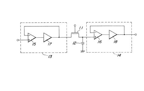
Referring to Fig. 1, there is illustrated a
sample holding circuit embodying the invention. While
the invention will be described in conjunction with a
CCD (charge coupled device) output circuit, it will be
appreciated that the invention is equally applicable to
other sample holding circuits.
The sample holding circuit comprises a sample
~93~3~
holding stage including a switching transistor 11 and a
capacitor 12. The switching transistor 11 has one
electrode connected to a point which corresponds to the
input of the sample holding stage and another electrode
5` connected to one terminal of the capacitor 12, the other
terminal of which is connected to ground. The junction
between the switching transistor 11 and the capacitor 12
is connected to a point which corresponds to the output
of the sample holding stage. The switching transistor
11 also has a gate electrode connected to a signal
source (not shown) which generates a series of timing
pulses to trigger the switching transistor 11 into the
conduction state at appropriate sampling times.
Conduction of the switching transistor communicates a
voltage signal to charge the capacitor 12.
The sample holding stage is shown as connected
at its input and output to voltage-follower circuits 13
and 14, respectively. The voltage-follower circuit 13
includes an operational amplifier 15 and a buffer
circuit 17. The operational amplifier 15 has positive
and negative inputs. The operational amplifier positive
input is connected to an input terminal for connection
to a CCD ~charge coupled device). The buffer circuit 17
is connected at its input to the output of the
operational amplifier 15. The output of the buffer
circuit 17 is connected to the input of the sample
holding stage and also through a negative feedback path
to the negative input of the operational amplifier 15.
The operational amplifier 15 is arranged to provide
Voltage-follower operation amplifying the difference
between the signals applied to the positive and negative
inputs thereof at a gain substantially equal to 1 with
introducing no DC level shift. Since the voltage-
follower circuit 13 has a high input impedance and a low
output impedance, there is no mutual influence between
the circuits. The buffer circuit 17 serves the function
12~3031
-- 5 --
of increasing the input impedance and reducing the
output impedance.
Similarly, the voltage-follower circuit 14
includes an operational amplifier 16 and a buffer
circuit 18. The operational amplifier 16 has positive
and negative inputs. The operational amplifier positive
input is connected to the output of the sample holding
stage. The buffer circuit 18 is connected at its input
to the output of the operational amplifier 16. The
0 output of the buffer circuit 18 is connected to an
output terminal for connection to another stage. The
buffer circuit output is also connected through a
negative feedback path to the negative input of the
operational amplifier 16. The operational amplifier 16
is arranged to provide a voltage-follower operation
amplifying the difference between the signals applied to
the positive and negative inputs thereof at a gain
substantially equal to 1 without introducing any DC
level shift. Since the voltage-follower circuit 14 has
a high input impedance and a low output impedance, there
is no mutual influence between the circuits. The buffer
circuit 18 serves the function of increasing the input
impedance and reducing the output impedance.
The operation is as follows. It is now
assumed that an analog signal, as indicated by the
waveform A of Fig. 2, is applied to the input terminal
of the sample holding circuit. The analog signal is
applied to the voltage-follower circuit 13 which
amplifies the analog signal at a gain of 1 and applies
the amplified analog signal to the sample holding state.
Since the voltage-follower circuit 14 introduces no DC
level shift, the amplified signal has no DC level
fluctuation. The sample holding stage samples and holds
values for the analog signal at appropriate sampling
times determined by the timing pulse signal applied to
the switching transistor gate electrode. The timing
1~3C~31
pulse signal is indicated by the waveform C of Fig. 3.
The sampled signal, which is indicated by the waveform B
of Fig. 3, is applied from the sample holding stage to
the voltage-follower circuit 14. The voltage-follower
circuit 14 amplifies the sampled signal at a gain of lo
Since the voltage-follower circuit 14 introduces no DC
level shift, the outputted signal has no DC voltage
fluctuation. The output signal is applied from the
sample holding circuit output terminal to the following
o stage.
The detailed circuit arrangement of the
voltage-follower circuits 13 and 14, which are
substantially the same in circuit arrangement, will be
described with reference to Figs. 4 and 5.
Referring to Fig. 4, the operational amplifier
15 or 16 includes a pair of NMOS transistors 41 and 4
connected in common source. Each of the NMOS
transistors 41 and 42 has an emitter connected to ground
through the collector-emitter circuit of a transistor 43
which has a gate electrode connected to a constant
voltage source 48b. The transistor 43 serves as a
constant curent source. The transistor 41 has a gate
electrode connected to an input terminal vin. The NMOS
transistor pair is connected to a constant voltage
source 48a through an active load which includes a pair
of transistors 44 and 45 each having an emitter
connected to the constant voltage source 48a and a base
connected to the collector of the transistor 41. The
transistor 44 has a collector connected to the collector
of the transistor 41. The transistor 45 has a collector
connected to the collector of the transistor 42. The
junction between the transistors 45 and 42 forms an
operational amplifier output terminal.
The buffer circuit 17 or 18 includes a pair of
NMOS transistors 46 and 47. The transistor 46 has a
base connected to the operational amplifier output
~Z93Q31
terminal; that is, the junction between the transistors
45 and 42. The transistor 46 also has a collector
connected to the constant voltage source 48a and an
emitter connected to the collector of the transistor 47.
The transistor 47 has a gate electrode connected to a
constant voltage source 48c and an emitter connected to
ground. The junction between the transistors 46 and 47
is connected to an output terminal vout and also through
a negative feedback path to the gate electrode of the
o transistor 42.
Referring to Fig. 5, the operational amplifier
15 or 16 includes a pair of PMOS transistors 51 and 52
connected in a common source fashion. Each of the PMOS
transistors 51 and 52 has an emitter connected to a
constant voltage source 58a through the
collector-emitter circuit of a transistor 53 which has a
gate electrode connected to a constant voltage source
58b. The transistor 53 serves as a constant current
source. The transistor 51 has a gate electrode
connected to an input terminal Vin. The PMOS transistor
pair is connected to ground through an active load which
includes a pair of transistors 54 and 55 each having an
emitter connected to ground and a base connected to the
Collector of the transistor 51. The transistor 54 has a
collector connected to the collector of the transistor
51. The transistor 55 has a collector connected to the
collector of the transistor 52. The junction between
the transistors 55 and 52 forms an operatonal amplifier
output terminal.
The buffer circuit 17 or 18 includes a pair of
PMOS transistors 66 and 57. The transistor 56 has a
base connected to the operational amplifier output
terminal; that is, the junction between the transistors
55 and 52. The transistor 56 also has a collector
connected to ground and an emitter connected to the
- collector of the transistor 57. The transistor 57 has a
031
gate electrode connected to a constant voltage source
58d and an emitter connected to a constant voltage
source 58c. The junction between the transistors 56 and
57 is connected to an output terminal Vout and also
through a negative feedback path to the gate electrode
of the transistor 52.
It is apparent from the foregoing that there
is provided, in accordance with the invention, a sample
holding circuit which can operate without introducing
any DC level shift. This feature is effective to
simplify circuit design. The sample holding circuit can
be arranged to have a wider dynamic signal range and a
wider circuit margin so that the circuit can operate on
a low-voltage power source. In addition, a plurality of
15 such sample holding circuits can be connected to form a
multistage sample holding circuit which can operate
without any voltage shift associated problems.
While two amplifier circuits have been shown
and described as being connected on the input and output
20 sides of a sample holding stage, it will be appreciated
that the sample holding circuit may includes at least
one amplifier circuit connected to the input and/or
output side of the sample holding stage.
Although this invention has been described in
25 conjunction with a specific embodiment thereof, it is
evident that many alternatives, modifications and
variations will be apparent to those skilled in the artO
Accordingly, it is intended to embrace all alternatives,
modifications and variations that fall within the scope
30 Of the appended claims.