Note : Les descriptions sont présentées dans la langue officielle dans laquelle elles ont été soumises.
~.Z~3~
IBM Docket No. BC9-87-003
COMPUTER SYSTEM HAVIN~ MODE INDEPENDENT ADDRESSING
DESCRIPTION
Technical Field
The present invention relates to a computer system
employing a processor having more than one addressing
mode. More specifically, the invention pertains to
such a computer system which is capable of running the
: same applications program in each of plural addressing
modes.
Background of the Invention
~ . .
Microcomputers (personal computers) are being re~uired
to perform more and more complex data processing tasks
while not suffering a degradation in response speed.
On the other hand, in order to perform the more sophis-
ticated tasks, additional device drivers, networking
programs, host attachment programs, session managing
programs, etc., must be loaded into the available
memory space. The amount of space left for the user's
applications programs is thus shrinking, forcing
undesirable trade-offs to be made among storage,
performance, and function.
To remedy this problem, microprocessors have lately
become available in which the amount of addressable
memory has been greatly expanded. For example, for the
Intel Corporation 8088/8086 microprocessor (hereinafter
a microprocessor will be reerred to for convenience as
a "CPU" - central processing unik), the amount of
-- 1 --
~.C9-87-003 2 i~38~
addressable memory is about 1 MB (MegaBytes), while for
the newer 80286 CPU, about 16 MB can be addressed.
The 80286, however, employs two different and mutually
incompatible addressing modes. The first mode, termed
the "rea]" mode, is exactly the same addressing mode
employed in the 8088/8086 CPU, and hence programs written
for a machine employing the 8088/8086 CPU, such as the
vast array of software written for the IBM~ PC computer
and compatibles, can be run in the real mode since the
same BIOS (Basic Input-Output System) can be used
directly. In the real mode, however, since the
addressing mode is in face the same as for the 8086/8088~
the amount of addressable memory is s~ill limited to
about 1 MB.
The second mode, termed the "protected" mode, employs a
different memory addressing scheme, and with this scheme
can address up to about 16 MB of memory. However, because
the addressing mode is indeed different, the earlier BIOS
cannot be used successfully, and hence computers which
have employed the 80286 CPU have not been able to
simultaneously take advantage of the increased amount of
available memory in the protected mode and run software
written for the 8086/8088 CPU.
Fig. 1 shows a memory map of a typical microcomputer
application employing an 80286 CPU and showing an example
of how the memory may be organized. Memory addresses in
the range of O KB (KiloBytes) to 40 KB are taken up by
the BIOS (Basic Input-Output System) and OS (Operating
System), the most famous examples being
,~.
lZ938;2~1L
.. .. .
IBM Docket No. BC9-87-003
PC DOS and MS DOS marketed by Microsoft Corporation.
The user is allocated the space from 40 KB to 640 KB in
both the real and protected mode. The video buffers
occupy 640 KB to 752 KB, and feature and planar ROMs
(Read-Only Memories) 752 KB to 1 MB. This is all the
memory that can be addressed in the real mode. In the
protected mode thou~l 15 MB of additional addressable
memory space is available to the user.
To better understand the problem solved by the inven-
tion, the two addressing modes will now be described in
more detail.
In both the 8088/8086 CPUs and in the real mode in the
80286 CPU, physical memory is addressed directly using
32-bit pointers. As shown in Fig. 2, each 32-bit
pointer is composed of a 16-bit offset (bits O to 15~
and a 16-bit segment (bits 16 to 31). The memory is
divided into 64 KB segments, and each of the 16-bit
segment values of the pointers corresponds directly to
one of these 64 KB segments in memory. That is,
pointer segment n, multiplied by 2 (equivalently,
shifted one place in hexadecimal), directly indicates
the address of the first eight-bit byte of data in
segment n of the memory, namely, the boundary between
~ segments n--l and n in physical memory. The offset, on
the other hand, indicates a displacement from the
boundary between segments n-1 and n.
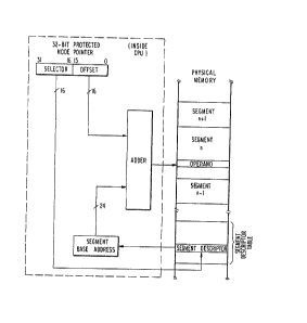
As indicated by the diayram of Fig. 3, to obtain the
20-bit value which directly addresses a given byte
location (operand address) in physical memory, the
-- 3
~3~?~
IBM ~ocket No. BC9-87-003
segment value is multiplied by 24 and added to the
offset value. This 20-bit address is applied directly
to the memory as an address.
In the protected mode of the 80286, the BIOS does not
use to physical memory in the form of segments and
offsets. ~oreov~r, the memory is not divided up into
64 KB segments. Instead, "virtual" memory addressing
is employed in which the addresses do not correspond
directly to distinct locations in physical memory. To
allow for more efficient use of the availab~e memory
space while still retaining relative ease of address-
ing, the memory is again divided into segments, but the
segments may be of variable len~ths. Generation of the
actual physical addresses is done internally to the
80286 CPU, out of reach of the user and BIOS.
The protected addressing mode will be explained in more
detail with reference to Fig. 4 of the drawings.
As .in the case of the 8088/8086 and real mode, the BIOS
addresses memory using a 32-bit pointer. In the
protected mode, the lower 16 bits ~bits O to 15) of the
pointer are also referred to as an offset. Because its
function is different than that of the segment in the
8088/8086 and real mode the upper 16-bit portion of the
pointer is termed a "selector". Instead of merely
multiplying it by 2 and adding it to the offset, the
selector is used as a pointer to a segment descriptor
contained in a segment descriptor table, which is
assembled in a predetermined area of the physical
memory. Each segment descriptor contains a 2~-bit
-- 4 --
~93~
.. .. . . . . .
IBM Docket No. BC9-87-003
value, which indicates the base address (lower boundary
address) of the corresponding segment in physical
memory. To obtain the actual address of a desired
operand in physical memory, the 24-bit segment descrip-
tor value retrieved by the selector is added to the
offset.
Because the selectors employed in the protected mode
thus have a function which is much different than arld
none~uivalent to that of the segments in the 8088/8086
and real mode, the BIOS designed for the 8088~8086 and
real mode, which uses segments in addressing, cannot
operate directly in the real mode, making it impossible
to run in the protected mode programs written to use
the BIOS developed for the 8088/8086 and real mode.
While such programs can of course be run on the 8028~
CPU in the real mode, it is a disadvantage not to also
be able to run them in the protected mode.
Objects~of the Invention
Accordingly, it is an object of the present invention
to provide a computer system and a method for operating
a computer system in which the above-discussed draw-
backs have been eliminated.
More specifically, it is an object of the invention to
provide a computer system and a method for operating a
computer system in which a single BIOS is capable of
supporting programs both in the protected mode and in
the real mode.
lZ93~2~
~ . .
. .. .
IBM Docket No. BC9-87-003
Summary of the Invention
In accordance with the above and other objects of the
invention, there is provided a computer system and a
method of operating a computer system having mutually
incompatible first and second addressing mode wherein,
for each addressing mode, a common data area table is
assembled containing pointers used to initiate the
various data transfer tasks and other basic in-
putjoutput operations which the operating system or
applications programs may need. Each pointer in the
; ~ common data area table for the first mode is e~uivalent
in function to a respective one of the pointers in the
common data area table for the secGnd mode. However,
the pointers in the two tables are assembled for their
respective addressing modes.
In the case of real and protected modes as discussed
above, the pointers for the real mode common data area
are each composed of a segment and an offset, and those
of the protected mode common data area are composed of
selectors and offsets. The offsets of the pointers in
the protected mode table which point to addresses
external to the common data area are identical in value
to those of corresponding pointers in the real ~ode
table, while the selectors correspond in physical
address to the segments of the corresponding pointers.
-- 6
3~3Z~
IBM Docket No. BC9-87-003
Brief Description of the Drawings
FIG. l is a memory map of an example of a computer
system employing a CPU having real and protected
addressiny modes.
FIG. 2 shows a portion of a main memory in the real
mode and illustrates how the memory is addressed using
offsets and pointers.
FIG. 3 depicts how segme.nts and offset values are
manipulated and added to produce physical memory
addresses in the real mode.
FIG. 4 shows a portion of a main memory in the protect-
ed mode and illustrates how the memory is addressed
using offsets and pointers.
~ FIG. 5 is a diagram showing how the BIOS code is
arranged in accordance with the present invention.
FIG. 6 is a map of a bimodal common data area in
accordance with the invention.
FIG. 7 is a flowchart showing in detail how the bimodal
common data area illustrated in FIG. 6 is assembled.
FIG. 8 is a flowchart showing an example of how a
device block pointer is obtained for a given logical
ID.
~. .
1~93~32~
.
IBM Docket No. BC9-87~003
FIG. 9 is a flowchart illustrating how a request is
made to the BIOS in the computer system of the inven-
tion.
Detailed Description of the Preferred
Embodiment of the Invention
~eferring first to the diagram of FIG. 5, there is
shown therein a memory map or the BIOS code employed
in the computer system of the invention.
The BIOS code is composed of three parts: POST, CBIOS
and ABIOS. POST (Power-On Self Test) is used for
performing initial self testing and other basic
start-up functions, including extracting the boot
record from the system disk and subse~uent loading of
the operating system into memory. CBIOS (Compatibility
Basic Input--Output System) contains the BIOS used by
applications programs for performing input-output
operations (transfers of data to and from memory,
peripherals, etc.) in the real mode only and in a
single-tasking environment. ABIOS (Advanced Basic
Input-Output System) contains the BIOS used by applica-
tions programs for performing input-output operations
in a bimodal, multi-tasking environment.
In accordance with the present invention, the ABIOS is
given the capability of operating either in the real
mode or the protected mode. The way in which this is
done is for the ABIOS to assemble bimodal CDAs (Common
Data Areas), one for the real mode and one for the
protected mode. The entries contained in the two CDAs
-- 8
~2~3~;;~glL
IBM Docket No. BC9-87-003
are identical in function, but in the real mode CDA the
pointers are described in terms of segments and off-
sets, while in the protected mode CDA they are de-
scribed in terms of selectors and offsets. If the
operating system intend~ to execute BIOS only in the
real mode, then only the real mode CDA need be assem-
bled and used, whereby BIOS-controlled data transfers
for applications programs take place in the previously
known manner for operations in the real mode. Before
the operating system can execute BIOS in the protected
mode, however, the protected mode CDA must be assem-
bled. By use of the protected mode CDA, since it is
functionally identical to the real mode CDA, programs
written for the real mode can successfully be run in
the protected mode at the user s option. Hence, by
providing the bimodal CDAs, the ABIOS code is essen-
tially "transparent" to the mode in which the user has
selected to run the CPU. The result is
mode-independent addressing for the applications
programs.
An example of bimodal CDAs is shown in accompanying
FIG. 6. The following abbreviations are used in FIG. 6
for simplicity:
LogicalID (LID) - Each LID corresponds to and
identifies a requested device. Each device available
to ABIOS has a LID associated therewith.
Device Block (DB) - The DB is a working storage
area allocated by the operating systèm which contains
~3~2~
IBM Docket No. BC9-87-003
hardware port addresses, interrupt levels, and device
state information.
Function Transfer Table (FTT) - The FT~ is a
permanent storage area allocated by the operating
system and which contains the pointers to each ~BIOS
function routine.
ABIOS Data Pointer (Data Ptr) - The data pointers
supply the ABIOS with addressability to particular
portions of memory in the bimodal environment. Exam-
ples are the pointers to the video ~uffers.
.
As can readily be appreciated from FIG. 6, in general,
the entries in the two CDAs are entirely identical in
function and in their place within the respective
tables; the only difference is that the pointers in the
real mode CDA are composed of segment and offset
values, and the pointers in the protected mode CDA are
composed of selectors and offsets. Thus, by merely
employing the CDA corresponding to the present operat-
ing mode of the CPU, so far as the remainder of the
BIOS, the operating system, and the applications
programs are concerned, all BIOS operations are per-
formed in the identical manner between the two modes.
That is, as illustrated in FIG. 6, the corresponding DB
pointer LID n in the two tables both point to the same
DB LID n, the corresponding data pointer 0 in the two
tables point to the same identical location in memory,
and the same function m pointers point to the same
identical function m.
-- 10 --
93~2~l ~
IBM Docket No. BC9-87-003
FIG. 7 is a flowchart describing in detail the manner
in which the two CDAs are assembled.
From the START point, the A~IOS is called to build the
systems parameters table in step 20. In step 21, ABIOS
is called to build the initiali~ation table. Next, in
step 22, memory space is allocated for the real mode
CDA, including the DBs, FTTs, and data pointers. In
subsequent step 23, an initial DB (InitDB) routine is
called for initial table entries to build the FTT, DB,
etc. Those having familiarity ~with the BIOS used in
the IBM A~r computer will understand the further details
of how steps 20 to 23 are implemented.
After it has been determined in step 24 that all
entries in the real mode CDA table are complete, in
step 25, memory space is allocated for the protected
mode CDA. In following step 26, in accordance with an
important aspect of the invention, an offset portion of
a DB pointer in the real mode CDA copied directly to
the corresponding entry in the protected mode CDA. For
~20 the offset value copied in step 26, in steps 27 and 28,
a selector is allocated whose physical address is equal
to the segment of the respective pointer in the real
mode CDA. In step 29, the selector is copied to the
corresponding position in the protected mode CDA to
complete the pointer.
With reference to steps 30 to 34, an FTT pointer is
assembled in a slightly different manner than the DB
pointers in steps 26 to 29 since the FTT pointers point
to other pointers within the CDA rather than addresses
~38~
IBM Docket No. BC9-87-003
external to the CDA. In step 30, a protected mode FTT
is allocated and, in step 31, a copy of the offset of
the corresponding protected mode FTT is copied to the
protected mode FTT pointer. In subsequent step 32, a
determination is made as to whether the protected mode
selector has been allocated. I not, in step 33, a
selector iq allocated which points to the FTT. In step
34, the selector is copied to the selector portion in
the protected mode CDA.
Similar to the assembly of the DB pointer in steps 26
to 29, in steps 35 to 38, a corresponding function
pointer is assembled in the protected mode CDA.
Step 39 tests to determine if all pointers of the FTT
have been completed. Steps 35 to ~9 are repeated until
all pointers of the ~TT have been assembled. Following
step 40 tests to determine whether all logical IDs, DB
pointers, and FTT pointers have been completed. If
not, the process loops back to step 26, and steps 26 -to
40 are repeated until all logical IDs, DB pointers, and
FTT pointers have been completed.
To finish the protected mode CDA, in step 41, the data
pointers (e.g., pointers to the video buffer) are
assembled. This is done in the same fashion as above.
In step 41, the offsek portion of a data pointer from
the real mode CDA is copied to the correspondin~ entry
in the protected mode CDA, and in step 42, a selector
is allocated having a physical address e~ual to the
segment in the corresponding real mode CDA entry. The
selector is copied into the protected mode CDA in step
- 12 -
~L2~3~
IBM Docket No. BC9-87-003
43. In step 44, it is determined if all data pointers
have been completed. If not, the process loops back to
step 41, whereupon steps 41 to 44 are repeated until
all data pointers have been finished. At that time,
assembly of both CDAs is completed.
To show an example of how the assembled CDA is used by
the ABIOS, FIG. 8 is a flowchart showing an example of
how a DB pointer is obtained ~rom the bimodal CDA ~or a
given logical ID.
First, the "current" CDA anchor pointer and the corre-
sponding logical ID are accessed in steps 60 and 61.
In step 62, the logical ID is multiplied by 23 (=8) to
obtain the offset for the DB pointer. Then, in step
63, the DB pointer can be accessed.
FIG. 9 is a flowchart showing how a program makes a
re~uest to the ABIOS.
First, in step 70, a re~uest block for the specific
re~uest at hand is allocated and filled in. In step
71, the "current" CDA anchor pointer is accessed. In
2~ subse~uent steps 72 and 73, the anchor pointer and the
RB pointer are saved in the stack frame using PUSH
instructions. The appropriate logical ID from the RB
is accessed in step 74. (There i8 of course a
one-to~one correspondence between logical IDs and
device entries in the CDA.) In step 75, the logical ID
is multiplied by 2 to obtain the o~fset of the DB
pointer (four bytès/pointer, two pointers). The
respective FTT pointer four bytes beyond the address of
- 13 -
8Zl
IBM Docket No. BC9-87-003
the DB pointer is accessed in step 76, and this ETT
pointer is saved to the stack frame using a PUSH
instruction in step 77. In step 78, the DB pointer is
saved to the stack frame, also using a PUSH instruc-
tion. Finall~v, in step 7g, the desired function is
called in the FTT.
Further applications are also contemplated within the
scope of the invention. For example, "patching" of the
BIOS code to effect changes thereto can be achieved
~ using the FTT pointers. That is, FTT pointers can be
inserted in the CDAs which cause redirection to patch
routines.
This completes the description of the preferred embodi-
ment of the invention. It is to be understood though
that while modifications can be made to the structure
and teachings of the present invention as deccribed
above, such modifications fall within the spirit and
scope of the present invention as specified in the
claims appended hereto.
.