Note : Les descriptions sont présentées dans la langue officielle dans laquelle elles ont été soumises.
~3006~38
DATA TERMINAL
BACKGROUND OF THE INVENTION
The present invention relates to a data terminal and, more
particularly, to a data terminal which is usable with a paging
receiver mounted thereon.
A paging receiver capable of receiving messages and
information is known in the communications art. This tYpe of
receiver may be connected to a data terminal havin~ a standard
communication interface or a printer mechanism in order to print
out a message or information as received by the receiver.
Generally, an antenna is built in such a pa~ing receiver and
used in an upright position so that it may be oriented
perpendicularly to an antenna of a transmit station. This is
because the electromagnetic wave from the antenna of the
-- transmit station is a horizontally polarized wave with respect toa ma~netic field and, therefore, the receive sensitivitY of the
receiver antenna cannot be enhanced unless the receiver antenna
is used in such an orientation as to traverse the magnetic flux of
the horizontallY polarized wave. However, when the paging
receiver is mounted on the data terminal, the only position of
2 0 the receiYer available is such that the receiver antenna is
oriented horizontally. This deteriorates the receive SensitivitY o~
the receiver antenna to a critical extent in practice use.
Another problem is that the receiver antenna is effected by
noise of a clock adapted to clock a central processing unit (CPU)
which is installed in the data terminal, further aggravating the
receive sensitivity of the antenna.
~30~88
70815-58
SUMMARY OF THE INVENTION
It is therefore an object of the present invention to
provide a data ter~inal which allows an antenna of a paging
receiver mounted thereon to achieve a high gain and high receive
sensitivi~y.
It is another obje~t of the present invention to provide
a generally improved data terminal.
A data terminal of the present invention comprises a
whip antenna, a resonance circuik connected to the whip antenna,
and a receiver accommodating portion for ac~ommodating a paging
receiver such that an antenna built in the receiver is coupled
with the resonance circuit. A ground of the resonance circuit and
a ground of circuitry which is mounted in the data terminal are
jointed with each other. In this constructiGn, the ground of the
circuitry serves as a reflector o~ the whip antenna to enhance the
antenna gain as well as the receive sensitivity. Preferably, the
antenna of the receiver is sufficiently remote from a clock
oscillating section for a CPU which is installed in the data
terminal, whereby clock noise generated by the clock oscillating
section is prevented from deteriorating the re~eive sensitivity.
The above and other objects, features and advantages of
the pre~ent invention will ~ecome more apparent from the following
detailed description taken with the accompanying drawings.
BRIEF DESCRIPTION OF THE DRAWINGS
Fiy. 1 is a schematic view showing a paging receiver in
a usual position for use;
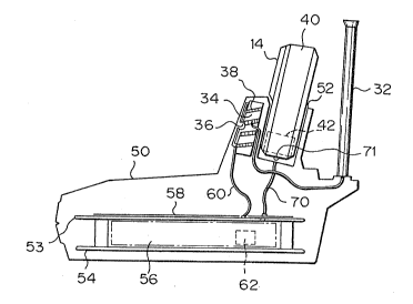
Fig. 2 is a partly sectional side elevation of a data
terminal embodying the present invention;
Fig. 3 is a block diagram schematically showing a
circuit arrangement of the data terminal as shown in Fig. 2; and
Fig. 4 is a front view of the data terminal of Fig. 2.
DESCRIPTION OF THE PREFERRED EMBODIMENT
To better understand the present invention, a brief
reference
C
30~688
will be made to a paging receiver in relation to a prior art data
terminal, shown in Fig. 1.
As shown in Fig. 1, a paging recei~er 10 includes an
antenna 12 which is used in a perpendicular position to an
antenna 2 2 which is located at a transmitting side 2 0, for the
reason as previously stated. SPecificallY, the electrornagnetic
wave from the antenna 22 of the transmitting side 20 is a
horizo~tally polarized wave with respect to a magnetic field so
that the receive sensiti~ity of the antenna 12 cannot be enhanced
unless the antenna 12 is used in such a manner as to traverse
the ma~netic flux of the horizontally polarized wave. In Fig. 1
the reference numeral 14 designates a display for displaying a
received message for information. A problem is that when the
receiver 10 is mounted on a data terminal, the onlY position
available is such that the receiver antenna 12 is oriented
horizontally, as shown in Fig. 4. This degrades the receive
sensitivity of the receiver antenna 12 to a critical extent.
Referring to ~igs. 2 to 4, a data terminal embodying the
present invention is shown which constitutes a solution to the
2 0 above-described problems. The data terminal, generally 5 0,
includes a whip antenna 3 2 which is located in a particular
position as shown in Fi~. 2. The whip antenna 32 is connected
to a resonance circuit 34 which is made up o~ a capacitor 36 and
a coil 38. As shown in Fig. 3, the whip antenna 32 and
resonance circuit 34 in combination serve as an external antenna
section 30. A paging receiver 40 is provided with an antenna 42
thereinside, whilc the data terminal 5 0 is provided with a
socket, or receiver accommodating section, 52 for
accommodating the receiver 4 0 thereinside. The socket i 2 is
positioned such that the receiver 40 put in the socket 52 causes
its antenna 42 to be coupled with the resonance circuit 34 of the
receiver 4 0 with respect to a magnetic field. Data is
interchanged between the receiver 4 0 and the data terminal 5 0
through a contact 71 and a connecting line 70, Fig. 3.
3 5 The whip antenna 3 2 seizes a desired electromagnetic wave
~3(~6~38
--4--
to cause the resonance circuit 34 to produce an induced current.
This induced current causes the coil 38 to develop a magnetic
flux which in turn induces a current in the antenna 42 of the
receiver 40. The current induced in the antenna 42 is fed as a
signal current to a reCeiViIlg section (RECEIVE) 44 as shown in
Fig. 3, whereby it is subjected to various kinds of processing
such as amplification and frequencY conYersion. The output
signal of the receiving section 44 is demodulated by a
demodulating section (DEMODULATE) 46 with the result that it
becomes a signal whose frequency lies in an audio frequency
band. The demodulated signal is delivered to an audio frequency
control section (AUDIO FREQUENCY CONTROL) 48 and therefrom
to the data terminal via the line 70.
As shown in Fig. 2, the data terminal 50 is provided with
two printed circuit boards 53 and 54 on which parts 56 are
mounted. A ground pattern 58 provided on the board 53 is
connected to the ground of the resonance circuit 34 by a
connecting line 60. A clock oscillating section 62 for clocking a
CPU is installed in a particular position of the data terminal, as
shown in Figs. 2 and 4. The socket 52 of the data terminal 50
is positioned sufficiently remotelY from the clock oscillator
section 62 so that the clock maY not influence the antenna 42 of
the receiver 40. In additiont the socket 52 is so positioned as
not to effect the attractive appearance of the data terminal.
The whiP antenna 3 ~ of the external antenna section 30
achieves a higher a~tenna gain than a loop antenna and others
since, as previously stated, the polarized wa~ve from the
transmit station is a horizontally polari~ed wa~e with resPect to
an electric field. The antenna gain is further enhanced by the
fact that the ground pattern 58 connected to the ground of the
resonance circuit 34 plays the role of a reflector of the whip
antenna 32. If desired, the inductance of the coil 38 of the
circuit 34 may be increased within a tunable range in order to
increase the magnetic flux which intersects the receiver antenna
35 42 and, thereby, the antenna gain. Because the antenna 42 and
~3~)~688
--5--
the clock oscillating section 62 are arranged as remote from each
other as possible, there is only a minimum of probability for tne
antenna 4 2 to pick up clock noise. Such offers an extra
improvement in the receiYe sensitivity of the antenna 42.
In summary, it will be seen that the present invention
provides a data terminal which enhances the receive sensitivity of
an antenna of a paging receiver by using a whip antenna and
connecting the ground of a resonance circuit of the terminal to
the ground pattern of circuitry which is mounted in the
terminal, the ground pattern serving as a reflector of the whip
antenna. The receiYe sensitivity is further enhanced because the
data terminal frees the receiver antenna from the influence of
clock noise.
Various modifications will become possible for those s~illed
in the art after receiving the teachings of the present disclosure
without departing from the scope thereof.