Note : Les descriptions sont présentées dans la langue officielle dans laquelle elles ont été soumises.
` ~3~7~
-l- RCA 85,045
~N ARR~NGEMENT FOR REDUCING RINGING
IN A FLYBACK TRANSFORMER
The invention relates to a high voltage power
supply of a television apparatus.
A conventional horizontal deflection circuit of a
television receiver typically includes a flyback
transformer. A high voltage such as, for example, an ultor
voltage, may be generated from a retrace pulse voltage in
the flyback transformer using a "diode split" arrangement.
In such arrangement, a segmented, tertiary high voltage
winding of the flyback transformer is coupled in series
with, for example, four rectifier diodes. One end terminal
of the tertiary or high voltage winding is coupled to an
ultor voltage terminal of a cathode ray tube (CRT). The
other end terminal of the high voltage may be coupled to a
filter capacitor that i.s coupled in parallel with a
resistor across which the average beam current is sampled.
The beam current representative voltage developed across
the resi~tor may be used for controlling, in a well known
manner, the operation of a beam current limiter.
The high voltage rectifier diodes conduct during
a short inter~al, close to the peak o~ the retrace pulse
voltage that is developed in the high voltage winding.
When the retrace pulse voltage starts sloping down, during
~5 the second half of retrace, the rectifier diodes become
abruptly n~nconductive, causing, disadvantageously, an
oscillatory ringing current to flow in the high voltage
winding, having initially a high amplitude with a gradually
decreasing envelope that may continue during the trace
interval.
The rinying current is generated by the energy
stored in the leakage inductance between a primary winding
and the tertiary winding of the flyback transformer. The
leakage inductance is required for obtaining a resonance
circuit that is tuned to, for example, the fifth harmonic
of the hoxizontal deflection frequency fH, in order to form
.
:~l30V74g~
-2- RCA 85,045
a low output impedance at the ultor voltage terminal. In
this way, a desirable high voltage stability versus beam
current is obtained.
As indicated before, the current in the tertiary
winding may, disadvantageously, continue in the form of
ringing current during trace. By transformer action the
parasitic ringing current appears also in the pximary
winding and affects voltages produced in other windings of
the flyback transformer. The ringing current may,
disadvantageously, disturb the deflection circuit,
resulting in dark vertical bars on the left side of the
displayed raster, particularly if an east-west raster
correction circuit is employed. Ringing voltage that is
produced in a secondary winding of the flyback transformer
may also disturb the phasing of the horizontal oscillator
resulting in distortion of a pattern of vertical raster
lines. Conse~uently, vertical lines of, for example, a
crosshatch pattern will not be perfectly straight. Such
dist.urbance in the horizontal oscillator synchronization
may occur in a deflection circuit in which a retrace
voltage in ~he secondary winding of the flyback transformer
is used for providing feedback synch~onization information
to the horizontal oscil].ator. It is, therefore, desirable
to reduce the amplitude and duration of the ringing current
in the tertiary, high voltage winding, during, for example,
the trace interval.
In some prior art circuits, a resistor coupled in
the current path of the current in ~he tertiary winding is
used to obtain sufficient damping action for the ringing
current. The added resistor may have a rather large value,
on the order o~ 20 to 40 kOhms. The narrow retrace current
pulse in the tertiary winding flows also through the added
ringing damping resistor. The result is a voltage drop of
between O.8kV and 1.5kV at, ~or e~ample, lmA average beam
current. Disadvantageously, this prior art solution also
increases signiicantly the output impedance at the ultor
voltage terminal. Furthermore, the added resistor,
disadvantageously, dissipates a high amount of power.
13(~
-3- RCA 85,045
A power supply, embodying an aspect of the
invention, o a television apparatus generates a high
voltage that is applied to a load of the television
apparatus. The power supply includes a source of an input
signal at a first frequency and a flyback transformer
having a high voltage winding. A high voltage that includes
a periodic flyback pulse having a period that is related to
the frequency of the input signal is generated in the high
voltage winding. The high voltage is applied to the load
during a flyback, first interval of the flyback pulse. The
high voltage is decoupled from the load following the first
interval. An impedance, coupled to the flyback transformer
conducts, during a second interval of the period of flyback
pulse, a ringing current that is produced in the
transformer such that during the second interval the
impedance dampens the ringing current. A switching
arrangement is coupled to the transformer for conducting a
portion of the ringing current through the switching
arrangement instead of through the impedance, that
substantially reduces the damping of the ringing current by
the impedance, during at least part of the first interval
of the flyback pulse.
In the Drawing:
FIGURE 1 illustrates a high voltage power supply
including a ringing current damper, embodying an aspect of
the invention;
FIGURES 2a-2c illustrate waveorms useful for
explaining the operation of the power supply of FIGURE l;
and
FIGURES 3a-3b illustrates waveforms of a power
supply without employing the ringing current damper of
FIGURE 1.
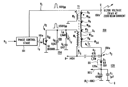
FIGURE 1 illustrates a high voltage power supply,
enbodying an aspect of the invention. In the power supply
of FIGURE l, a horizontal deflection circuit 250 that
provides horizontal deflection for a CRT, not shown,
includes a switching transistor Ql operating at a
horizontal frequency fH and an anti-parallel coupled damper
:~L30~'7fl~
-4- RCA 85,045
diGde DQl. A retrace capacitance CR is coupled in parallel
with transistor Ql and diode DQl. A deflection winding LH
is coupled in series with an S-shaping trace capacitance
Cs, forming a circuit branch that is coupled in parallel
with each of transistor Q1, diode DQl and retrace
capaitance CR to form a retrace resonant circuit 100
during horizontal retrace.
A phase-control stage 101 that includes a
horizontal oscillator and a phase detector, not shown in
the drawing, is responsive to a horizontal synchronizing
signal Hs. Signal Hs is derived from, for example, a video
detector of a television receiver, not shown in the
drawing. Stage 101 applies a drive signal lOla to a
base-emitter junction of a transistor Ql for producing a
base drive current ib at the horizontal frequency fH .
Current ib causes the switching operation in transistor Ql
that causes a deflection current iy to flow in windirlg LH.
A primary wind.ing W1 of a flyback transformer T1 is coupled
between a source o~ a B~ suppl~ voltage and the collector
of ~ransistor Ql. A secondary winding W2 oE -transormer Tl
is coupled to stage 101 to provide a eedback retrace
signal V1 produced by the switching operation of transistor
Q1. Stage lOl generates drive signal lOla, causing
horizontal deflection current iy to be exactly phased to
signal Hs.
A retrace voltage V2, generated at a junction
terminal between primary winding Wl of transformer T1 and
the collector of transistor Q1, is magnetically coupled to
winding segments W3a/ W3b/ W3C and W3d of g
tertiary, high voltage winding W3 of transformer T1. The
retrace pulse voltages in winding segments W3a - W3d are
rectified using rectifying diodes Da-Dd. Diodes Da-Dd and
winding segments W3a-W3d that are alternately coupled in
series, form a diode split arrangement 150 having an end
terminal 150b at which ultor voltage U is developed. The
other end terminal, a terminal 150a, is coupled to a
cathode of a diode D1 of a current ringing damping
arrangement 120, embodying an aspect of the invention. The
~3~
-5- RCA 85,045
anode of diode D1 is coupled to a terminal 120a of a beam
current sampling resistor Rl , coupled in parallel with a
filter capacitor C1. The other terminals of resistor R
and of capacitor Cl are coupled to a common ground
potential G.
Diode Dl is conductive close to the peak of the
retrace voltage developed in winding W3. Diode Dl is poled
in the same direction as diodes Da-Dd. A beam current
indicative voltage BCL at a low level is developed at
terminal 120a and applied to a conventional beam current
limiter, not shown. Current ringing damping arrangement
120 includes a damping resistor R2 coupled to receive the
B+ supply voltage of, illustrati~ely, ~145V and to apply
the B+ supply voltage to terminal 150a of Diode Dl.
FIGURES 2a-2c illustrates waveforms useful in
e~plaining the operation of the high voltage power supply
of FIGURE 1. Similar numbers and symbols in FIGURE 1 and
in 2a-2c indicate similiar items or functions.
At the beginning of each retrace interval,
designated as time tl in FIGUREs 2a-2c, transistor Q1 of
FIGUR~ 1 becomes nonconductive, causing a retrace voltage
V2 to develop across primary winding Wl of flyback
transformer Tl and a retrace voltage V1 to develop across
winding W2. The waveform of retrace voltage V2 is similar
in shape to that of voltage ~1 of FIGURE 2a. The
peak-to-peak amplitude of voltage V2 is approximately 1150V
and that of voltage V1, 60V. Similarly, corresponding
retrace voltages are developed across each winding segmen-t
W3 -W3d of tertiarY winding W3.
Throughout trace, and at time tl of FIGURES
2a-2c, the beginning of retrace, diode Dl of FIGURE 1 is
back biased by the +145V that is applied via resistor R2 to
the cathode of diode D1. As a result, a voltage V3 at
terminal 150a has an aveLage value that is equal to +145V
during trace and at the beginning time, tl, of retrace of
FIGURE 2c.
As the level of the retrace voltage at winding
segment W3d increases, during the first half of retrace, a
~3~7~4
-6- RCA 85,045
current i2, flowing in winding W3, increases. Current i2
that also flows through resistor R2 causes voltage V3 to
decrease until diode Dl becomes forward biased and clamps
voltage V3 to approximately zero volts, as shown at time t2
in FIGURE 2c. The further increasing current i2 of FIGURE
2b in winding W3 of FIGURE 1 flows mainly through forward
biased diode Dl and b~passes resistor R2, during interval
tc of FIGURE 2c. Therefore, advantageously, resister R2
does not increase the output impedance at ultor terminal
150b during interval tc of FIGURE 2c. During interval tc,
current i2 of FIGURE 1 charges the ultor capacitance formed
by the CRT, not shown.
During interval tc of FIGURE 2c, current i2 f
FIGURE 2b is not damped since conductive diode Dl of FIGURE
1 bypasses resistor R2. When diode Dl is conductive, the
impedance developed across resistor R2 is formed by the
series arrangement of the "ON" resistance of diode Dl and
the impedance of capacitor Cl that is low at the horizontal
frequency fH and its harmonics. Consequently, during
interval tc f FIGURE 2c, current i2 of FIGURE 2b is an
undamped oscillatory current. Current i2 oscillates at the
fif~h harmonic of the fundamental frequency fH of voltage
V1 o FIGURE 2a. The oscillation frequency is determined
in acc~rdance with ~he resonance ~re~uency to which a
resonance circuit that includes the leakage inductance of
transformer T1 is tuned. The resulk is that the output
impedance at ultor terminal 150b is advantageously low,
that provides better ultor voltage regulation as a function
of beam current than if resistor R2 were not bypassed.
During interval tc f FIGURE 2c, voltage V3 is
clamped to the small, negative level of voltage BCL
developed across resistor R1 and capacitor C1 of FIGURE 1.
As indicated before, voltage BCL is used by a beam current
limiter, not shown, for limiting excessive beam current in
the CRT. Thus, advantageously, damping arrangement 120 can
be used together with the beam current sampling resistor
R1. At the end of interval tc of FIGURE 2c, diodes Da, Db,
Dc, and Dd become non-conductive, and ringing current i2 f
~3C~0~7~4
-7- RCA 85,045
FIGURE 2b produces a high amplitude of ringing in voltage
V3 of FIGURE 2c, developed across damping resistor R2 f
FIGURE 1.
During the second part of retrace that follows
interval tc, current i2 of FIGURE 2b and the B+ supply
voltage cause diode D1 of FIGURE 1 to be back biased.
Therefore, during the second part of retrace and also
during trace, diode D1 is back biased, causing current i2
to flow mainly through damping resistor R2 that is coupled
in series with winding W3. Consequently, in accordance
with an aspect of the invention, energy dissipating
resistor R2 dampens the ringing component of current i2 f
FIGURE 2b. The result is that the potentially ill effects
of such current ringing, as explained before, axe
substantially reduced.
FIGURES 3a and 3b illustrate waveforms of a
modified arrangement of FIGURE 1 in which resistor R~ of
FIGURE 1 is removed, in which a larger resistor of lOKQ is
substituted for resistor R1 of FIGURE 1 having a value of
4.7 KQ and in which diode Dl of FIGURE 1 is replaced by a
jumper wire 55, all as shown by dash lines in FIGURE 1.
Such modi~ied arrangement does not include damping
arrangement 120 of the inve~tioll. Similar numbers and
symbols in FIGUREs 2a-2c and in FIGUREs 3a-3b indicate
similar items or functions.
In order to obtain a predetermined level of
voltage BCL at a corresponding level of current i2 that
are, each, the same in both the modified and the unmodified
arrangement of FIGURE 1, the value of resistor R1, in the
unmodified arrangement, is smaller. This is so because of
the higher DC voltage level developed in resistor R1 as a
result of the rectification caused by diode D1 in the
unmodified arrangement.
By comparing FIGUREs 3b and 2b, for e~ample, it
can be seen that the amplitude of the ringing current
component of current i2 of FIGURE 1 during trace is,
advantageously, significantly lower when damping
...... .. ..
.
13U~744
-8- RCA 85,045
arrangement 120 is included in the high voltage power
supply.