Note : Les descriptions sont présentées dans la langue officielle dans laquelle elles ont été soumises.
:13U;~
PHN 11.845
A method of manufacturing a display device and a display device made by
the method.
The present invention relates to a method of making a
display device, such as a cathode ray tube, a liquid crystal display
device and a solid-state electroluminescent display device, and to a
display device made by the method. More particularly the invention is
concerned with reducing the reflectance of a viewing screen.
Display devices have to be capable of being viewed under
varying lighting conditions. However since the brightness of an image
being displayed on a device is limited, the contrast must be as high as
possible, so that even under conditions of high-intensity ambient-light
levels a clearly visible picture is presented to the viewer.
Consequently display device manufacturers endeavour to increase the
contrast of such devices and one technique is to reduce the amount of
ambient light reflected by the glass faceplate, glass having a
reflectance of 4.9~.
As the sensitivity of the human eye (see Figure 3 of the
accompanying drawings) has a peak sensitivity at about 550 nm
(nanometers) and decreases to zero below 400 nm and above 700 nm, then
this is the part of the spectrum which is of interest.
There have been prior proposals relating to reducing
the reflectance from cathode ray tube faceplates. European Patent
Publication 0 131 341 (PHN 10.737) discloses mechanically roughening the
outer surface of a cathode ray tube faceplate and vapour depositing
a single layer of A/4 thick magnesium fluoride (MgF2), where A is the
peak sensitivity wavelength, that is about 550 nm. The refractive
indices of air, glass and MgF2 are respectively 1.0, 1.57 and 1.39.
Although such an arrangement reduces the reflectively at the faceplate,
it does have some disadvantages including (1) the reduction in
reflectivity is a maxima at the peak sensitivity wavelength and is
progressively less on either side of this peak sensitivity wavelength
and (2) in order to obtain a layer having the required degree of
hardness the MgF2 has to be deposited onto a heated substrate.
Typically the minimum temperature for the substrate, that is the
13(~31~9
PHN 11.845 2
faceplate, is 200C but a temperature of 250C is preferable. As the
heating of the faceplate takes place under vacuum, the heat transfer is
by radiation which is slow and takes about one hour. It is possible to
vapour deposit layers of MgF2 at lower temperatures but these layers
do not have the required degree of hardness to be of use as anti-
reflection coatings. Such layers cannot be hardened further by annealing
after deposition.
In the description and claims reference is made to
materials having low, medium and high refractive indices (n). These
relative terms are related to the refractive index of the material, for
example glass, forming an optically transparent faceplate panel. For a
glass having n = 1.5 then a low value for n may be equal to or less than
1.5, a medium value for n may lie in the range of greater than 1.50 and
less than 1.80, and a high value for n may be e~ual to or greater than
1.80.
The reflectivity characteristic of the anti-reflection
coating should be such that in the visible part of the spectrum it
has a substantially constant value and ideally be zero. In the case of a
laser it is known to use an interference filter comprising a first layer
having a relatively high refractive index applied to the faceplate and a
contiguous second layer having a relatively low refractive index. Such
an arrangement is known as a V-coating because the reflection
characteristic is of generally V-shape with the vertex or minimum
reflectance at the wavelength of the laser light. The flanks of the V-
characteristic can be modified using a three layer interference filtercomprising a first layer of a material, such as Al203, having a
medium refractive index, a second thicker contiguous layer of a
material, such as Tio2, having a relatively high refractive index and
a third contiguous layer of a lesser thickness than the second layer and
being of a material, such as MgF2, having a relatively low refractive
index. This coating is known as a W-coating because it has a wider
characteristic with two minima, one on either side of the centre
wavelength. As far as is known such anti-reflection coatings are vapour
deposited onto substrates heated to about 300C in order to obtain the
required degree of hardness and scratch resistance. The materials used
in making these layers cannot be hardened by subsequent annealing.
It is an object of the present invention to provide a
13~3115~
PHN 11.845 3
scratch resistant anti-reflection coating on a display device by a
method which does not require special heating of a substrate (or
faceplate) above the ambient temperature prevailing inside the
processing vessel.
Accoxding to the present invention there is provided a
method of making a display device, comprising providing a hardened anti-
reflection coating on an external surface of a faceplate panel, said
coating being provided by vacuum evaporating at least 3 filter layers on
to the faceplate panel in an evaporation apparatus which is at ambient
temperature, the material of one of said layers having a high refractive
index with respect to that of the material of the faceplate panel and
the material of another one of said layers having a low refractive index
with respect to that of the material of the faceplate panel, the
materials comprising said layers having a medium degree of hardness
after evaporation, and hardening said layers by annealing outside the
evaporation apparatus at an elevated temperature.
Although an acceptable anti-reflection coating can be
made from 3 layers, it is preferred that the coating comprises 4 or more
layers in order to be less dependent on the material choice.
~y selecting materials such as niobium pentoxide
(Nb205), silicon oxide (Si~2) and aluminium oxide (Al203) it
is possible to evaporate them at ambient temperatures, of the order of
80C, prevailing in the vacuum evaporation vessel, to produce layers
of a medium degree of hardness which can then be made to ha~e a high
degree of hardness by annealing at elevated temperatures outside the
evaporation vessel. Avoiding having to heat the substrate (or
faceplate) saves heating time in a vacuum. Additionally, if the
annealing step is part of the normal processing of the cathode ray tube
this time saving becomes effective.
Producing anti-reflection coatings this way has been
found to produce filter layers with little or no crazing.
If desired the outer surface of the faceplate may be
mechanically roughened in order to reduce the specular reflectance of
the faceplate.
In one embodiment of an anti-reflective four layer
coating the first and second layers applied to the faceplate are each
thinner than the outermost layer. The first layer has a high refractive
:1.~31~S~
- 4 - 20104-8361
index and may comprise Nb2O5. The outermost layer may comprise
SiO2 as may be the second layer which in any event comprises a
material having a refractive index of between 1.4 and 1.8.
In this embodiment of a display device made in accor-
dance with the present invention, the first and second layers of
a four layer anti-reflection coating each have a thickness of
the order of ~/8, the third layer has a thickness of the order of
~/2 and the outermost layer has a thickness of the order of ~/4,
where ~ is equal to a desired central wavelength selected from the
eye sensitivity curve.
The present invention also relates to a display device
having an optically transparent faceplate, an anti-reflection
coating on an external surface of the faceplate, the anti-
reflection coating comprising at least three layers of materials
which are depositable at ambient temperature and hardenable by
subsequent annealing, said layers having been hardened by annealing,
the material of one said layers having a high refractive index
with respect to that of the material of the faceplate and another
one of said layers having a low refractive index with respect to
that of the material of the faceplate.
The display device may comprise a cathode ray tube
such as a colour cathode ray tube, a projection television tube
in which case the centre wavelength is the wavelength of the phos-
phor, a data graphic display (D.G.D.) tube or an oscilloscope
tube.
The present invention will now be described, by way of
~3U311~
- 4a - 20104-8361
example, with reference -to the accompanying drawings, wherein:
Figure 1 is an elevational view of a cathode ray tube
with a portion of its wall broken away,
Figure 2 is diagrammatic cross-sectional view through
a portion of the faceplate structure having an anti-reflection
coating thereon,
Figure 3 is a sensitivity curve of a human eye,
Figure 4 shows a number of reflectance curves which
are useful for explaining the performance of different types of
anti-reflection coatings,
Figures 5 and 6 illustrate the reflectances of anti-
reflection coatings made by the method in accordance with the
invention and having 4 and 7 layers, respectively, and
Figure 7 is a diagrammatic view of an apparatus for
carrying out the method in accordance with the present invention.
13~3~1~
PHN 11.845 5
In the drawings, corresponding reference numerals have
been used to indicate similar features.
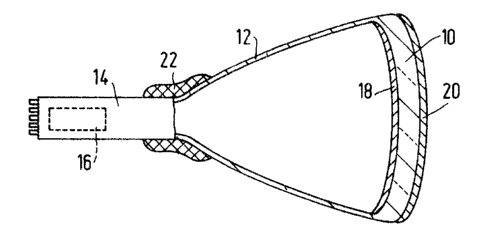
The cathode ray tube shown in Figure 1 comprises an
envelope formed by an optically transparent faceplate panel 10 which is
connected to a conical portion 12, a neck 14 is connected to the conical
portion 12. An electron gun 16 is disposed within the neck 14. A
cathodoluminescent screen 18 is provided on the inside of the faceplate
panel 10. An anti-reflection coating 20 is provided on the outside
surface of the faceplate panel 10 which is composed of a mixed alkali
glass substantially free of lead oxide (PbO). An electron beam (not
shown) produced by the electron gun 16 is scanned over the screen by a
deflection coil assembly 22 provided at the neck-conical portion
transition of the envelope.
The illustrated cathode ray tube may comprise a
monochrome tube, a PTV tube or an oscilloscope tube. However the
invention can be applied to a shadow mask display tube or to any other
display device because it is primarily directed to enhancing the
contrast of an image by reducing reflections from the outer surface of
the faceplate.
The faceplate structure and anti-reflection coating 20
shown in Figure 2 have not been drawn to scale. The illustrated anti-
reflection coating 20 comprises four contiguous layers 26, 28, 30, 32
applied by vacuum evaporation at ambient temperatures onto the faceplate
panel 10. The layers 26 to 32 have different thickness and the layers 26
25 and 30 are of a material, such as Nb205, having a relatively high
refractive index and the layers 28 and 32 are of a material, such as
SiO2 having a relatively low refractive index. Although the precise
thickness of each of the layers 26 to 32 is selected having regard to
the refractive index, n, of the material of each layer and the optical
performance required, the thickness of each of the layers 26, 28 is of
the order of A/8, that of the layer 30 is of the order of ~/2 and
that of the layer 32 is of the order of Al4, where A is equal to the
desired centre wavelength selected from the eye sensitivity curve shown
in Figure 3. One advantage of having layers of different thicknesses is
that interference effects are reduced. Materials such as Nb205 and
sio2 form medium hardness layers when evaporated on to the unheated
faceplate panel 10 at ambient temperature which is of the order of
13(~31~S~
PHN 11.845 6
80C. However unlike materials such as MgF2 these layers can be
hardened subsequently by high temperature annealing to make them scratch
resistant.
In fabricating such a 4-layer coating, it has been found
S desirable to deposit a layex of Nb205 onto the glass and have the
outermost low refractive index layer comprise SiO2. However such an
arrangement is not obligatory.
The second layer 28 may comprise a different material
from SiO2, such different materials including Al203, MgO,
or CeO2. Some of the criteria for the selection of the material for
this layer are that it has a refractive index between 1.4 and 1.8, and
that it can be evaporated as a relatively hard layer which can be
annealed to a harder layer subsequently.
Figure 3 is a sensitivity curve 34 of a human eye. The
abscissa is wavelength, A, in nanometres (nm.) and the ordinate is
calibrated in arbitrary units. The curve is generally Gaussian and has a
peak value at about 550 nm.
Figure 4 shows graphs of wavelength, A, against
reflectance (R1 in per cent of glass and the reflectances of coatings
having 1, 2 or 3 filter layers. The reflectance of glass is shown by a
horizontal line 36 having a reflectance value of 4.~%.
In order to eliminate reflections at least over the
range of wavelengths to which the eye is sensitive, an anti-reflection
coating would ideally have a rectangular characteristic 38 shown in
broken lines. A typical single layer anti-reflection coating has a
characteristic shown by the chain-dot line 39 which has a minimum
reflectance value at about 550 nm. A typical double layer V-coat filter
characteristic is shown by the chain-double dot line 40 and has a
minimum or zero reflectance over a short range of wavelengths which
makes such an anti-reflection coating suitable for use on lasers. The
characteristic of a 3-layer W coating is shown by the line 42. The
presence of a third layer has the effect of pulling the flanks of the V-
characteristic 40 sideways to produce a curve which is closer to the
idealised characteristic. By providing 4 or more layers the reflectance
curve obtained approximates closer to a rectangle. In the case of a 4
layer coating, the layer thicknesses are of the order of A/8, A/8, A/2
and A/4 beginning from the glass substrate.
13(~311~
P~N 11.845 7
Figure 5 is a graph of the reflectance (R) of a 4-layer
anti-reflective coating made by the method made in accordance with the
present invention. The anti-reflective coating comprises a first layer
of Nb205, which has a high refractive index t2.14) and an optical
thickness tn.d.lA) 0.079, applied to the faceplate panel, a second layer
of SiO2, which has a low refractive index t1.43) and an optical
thickness 0.092, a third layer of Nb205 which has an optical
thickness of 0.577 and an outermost layer of SiO2 which has an optical
thickness of 0.249.
Figure 6 is a graph of the reflectance (R) of a 7-layer
anti-reflective coating made by the method made in accordance with the
present invention. The coating comprises alternate layers of sio2 and
Nb205 whose refractive indices (n) after annealing are 1.45 and
2.10, respectively. The innermost and outermost layers are of SiO2.
The coating construction and optical thicknesses of the respective
layers comprise:
tnd/A)
Glass --
Layer 1 SiO2 0.534
2 Nb25 0 059
3 Si2 0 119
4 Nb25 0.491
SiO2 0.435
6 Nb25 0.376
7 SiO2 0.193
Air ~~
The illustrated curve is flatter compared to that shown
in Figure 5 and that over the wavelength range specifiedr the
reflectance is less than 1% and in this respect approaches the ideal
curve 38 more closely.
In the case of a 3-layer anti-reflective coating, an
exemplary filter has a first layer of Al203 tn=1.63) and having an
optical thickness of 0.25, a second layer of Nb205 and having an
optical thickness of 0.50 and a third, outermost layer of SiO2 and
having an optical thickness of 0.25.
Figure 7 illustrates diagrammatically an embodiment of
the evaporation apparatus in which the filter layers of the anti-
~L3(~311~
PHN 11.845 8
reflection coating are deposited on the faceplate panel 10. Theapparatus comprises a Balzers BA510 optical coater 44 which includes a
bell shaped cover 46 which is movable vertically relative to a base 48
for the introduction of, and removal of, faceplate panels 10 mounted in
a rotatable support 50. The optical materials, such as Nb205 and
SiO2, are evaporated from an~Airco - Temescal 8 kW four pocket
electron qun 52. The electron gun 52 is arranged eccentrically in the
space defined by the cover 46 in order to obtain a homogeneous thickness
distribution on the rotating faceplate panels 10.
A pumping system 54 consisting of a DIFF 1900 oil-
diffusion pump and a DUO 35 rotary are coupled to the interior of the
evaporation apparatus by way of an entry port in base 48. The effective
pumping speed for N2 is 600 l/s and the ultimate pressure is
5 x 10 7 Torr. A liquid N2 Meissner trap is built-in for extra
pumping speed for H20 during deposition.
The deposition rates are controlled with a quartz-crystal
thickness monitor 56 (for example a Leybold IC-6000). The optical layer
thicknesses nd is measured during evaporaton, using an optical monitor,
for example a monitor made by Dynamic Optics, which comprises a light
source 58 which shines its light through a window 60 in the bell cover.
This light is reflected by an inclined mirror 62 through a monitoring
glass 64 carried by the rotatable support 50. The light transmitted by
the monitoring glass 64 is filtered by a monochromatic filter 66 before
impinging on a detector 68 of the monitor. The monitor 56 follows the
transmission and its interference effects at chosen wavelengths.
An inlet 72 is provided in the cover 46 for the
introduction of a mixture of argon ~Ar) and oxygen (2) under reduced
pressure during substrate cleaning and of oxygen only during
evaporation. An aluminium rod 74 is mounted inside the cover 46 and is
connected to a power supply unit 76 in order to establish a glow
discharge during the substrate cleaning phase.
In carrying out the method in accordance with the present
apparatus, the faceplate panels, which may have had their external
surfaces mechanically roughened by a method as disclosed is European
Patent Publication 0 131 341, details of which are included by way of
reference, are mounted in the rotatable support 50. The bell cover 46 is
lowered onto the base 50.
I ~ ~a rk
13u311~
PHN 11.R45 9
Initially the system is evacuated to a pressure of the
order of 5 10 6 Torr. Then the faceplate panels are cleaned using a
glow discharge in an atmosphere of 900 Ar/10~ 2 at a pressure of
10 1 to 10 2 Torr. The glow discharge current is of the order of 100
mA and the cleaning operation lasted for 15 minutes.
Then the evaporation phases are carried out beginning
with Nb205 under a partial oxygen pressure of 3.10 4Torr at a rate
of 0.7 nmls (nanometres/sec). Once the desired thickness of Nb205
has been deposited, the actual thickness being monitored using the
thickness monitor 56, the electron gun 52 is switched to sio2 which is
deposited under a partial oxygen pressure of 3.10-4 Torr at a rate of
1 nm./s. At the completion of the evaporation phases the evaporation
apparatus is vented and the faceplate panels are removed.
Annealing of the coating 20 takes place subsequently at a
temperature of 450C in air for about 1.5 hours. It is advantageous
from the point of view of economising on the time required to make a
cathode ray tube to anneal the coating during the normal processing of
the cathode ray tube.
Annealing not only hardens the layers but also changes
their refractive indices. Accordingly when designing an anti-reflection
coating, the performance specification must be related to the filter
coating after annealing.
Although the coating 20 may comprise at least 3 layers,
four or more layers will provide a more practical anti-reflection
coating because the material choice is greater.