Note : Les descriptions sont présentées dans la langue officielle dans laquelle elles ont été soumises.
PHASE DIFFERENCE ADJUSTING CIR~UIT
BACKGROUND OF THE INVENTION
The present invention relates to a phase adjusting
circuit for adjusting the phase difference between
signals that are supplied through different transmission
lines.
A parallel transmission system for distributing
signals to a plurality of transmission lines improves
the reliability of communications. In -this sys-temr
delays differ from one transmission line to another so
that it requires to provide a phase adjusting circuit
on the reception side in order to adjust the delays 03^
phase difference.
One example of the conventional phase adjusting
circuit is described in Japanese Patent Publication
15 NoO 61-24852 (24852/86) by Nishiwaki. The Nishiwaki's
circuit comprlses memories each being associated with
the input line and read and write control circuits
wherein phase adjustment is performed~ by independently
writing input~data~ into each memory and orderly reading
data from each memory under control of the write and read
control circuits. Such a conventional phase adjusting
circuit, however, requires memories and read and
write control circuits for each input line, thus there
has heen a drawback that the circuit scale tends to
75~
66446-472
become large. In addition, there is al50 a drawback that the
writiny and reading operations of ~he memories have to be
controlled separately, resultlng in complicated operations.
SUMMARY GF THE INVENTION
It is an object of the present invention to provide a
phase adjusting circuit with small circuit scale and simplified
operations.
In accordance with one aspect of the present invention,
there is provided a phase adjusting circuit for adjusting the
phase relation between input data s~rings supplied via input
lines, comprising: sync detecting means provided for each of said
lines, for generating frame sync detection signals by detecting
frame sync signals of said input data strings; means for detecting
a firsk data string having a largest delay in the input data
strings; phase difference detecting means for detecting phase
differences between said first data string and remaining data
strings other than the first data strlng to produce phase
difference signals for said remaining data strings; line
connecting signal generating means responsive to said phase
difference signals ~or generating line ~onnecting signals;
variable delay means responsive to said phase difference signals
for outputting delayed data strings by giving delays to said
remaining data strings; first switching means responsive to said
line connecting signals for delivering said remaining data strings
to said variable delay means and for outputting said first data
string a.s it is; and second switching ~eans responsive to said
line connecting signals ~or delivering said first data string and
~3~S7~
66446-472
said delayed data st~ings into output lines ~orresponding to said
input lines.
According to another aspect of the present invention~
there is provided a phase adjusting circuit for adjusting a phase
difference between first and second input data strings supplied
through first and second input lines, comprising: sync detecting
means for generating a first and a second sync detection signals
by detecting sync signals ~rom said first and second input data
strings; phase relation signal generating means responsive to said
first and second sync detection signals for generating a phase
relation signal representing the phase relation between said first
and second input data strings; phase difference detecting means
for generating a phase di~ference signal indicative of the pha~e
difference between said first and second data strings; ~irst
switching means responsive to said phase relation signal for
switchiny said first and second input data strings to produce
first and second sw.ttched data s~rings; variable delay means
responsive to said phase difference signal for delaying said
second switchçd data s~ring to produce a delayed data string; and
second switching means responslve to said phase relation signal
for delivering said delayed data string and said switched first
data string to output llnes corresponding to said input lines.
BRIEF DE5CRIPTIO~ OF THE DRAWINGS
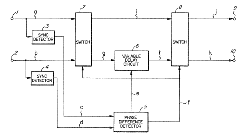
Fig. 1 is a block diagram showing an embodiment of the
present invention;
Fig. 2 is a circuit diagram showing an example of the
phase difference detecting circuit in Fig. 1;
5~
6~6-~72
Figs. 3a to 3k are waveform diagr~ms for explaining the
operation of Ihe circuit shown in Fig. 1; and
Figs. 4a to 4k are ~aveform diayrams for explaining the
operation of the circuit shown in Fig. 2.
DETAILED DESCRIPTION OF THE PREFERRED EMBODIMENT
Fig. 1 is a block diagram showing an embodiment of the
present lnvention, and Fig~. 3a to ~k are ~aveform diagrams for
explainlng the operation of Fig. 1. In the present embodiment the
case will be described in which both of the input and ou~put have
ld two lines. Further, reference letter in parentheses in the
caption to Flgs. 3a to 3k corresponds to the same letter appearing
on a signal line in Fig. .1, and it is assumed the phase relation
3a
b
~L3g:~5~5~
between the da-ta strings a and b is that the phase of the
data strlng a is in advance of the data string b.
In Fig. 1, a first inpu-t data string a (Fig. 3a)
from a first input terminal 1 is supplied to a firs-t sync
S detector 3 and a first switch 7, whereas a second input
data string b (Fig. 3b) from a second input terminal 2
is supplied to a second sync detector 4 and the first
switch 7. The first sync detector 3 detects the frame
sync signal or the frame pattern of the first input data
string _, and outputs a first frame detection pulse c
(Fiy. 3c) to a phase difference detec-tor ~PDD) 5. The
second sync de-tec-tor ~ detec-ts the frame sync signal of
the second input data string b, and ou-tpu-ts a second
frame detection pulse d (Fig. 3d) to the PDD 5. Both
lS the first and the~second frame detection pulses c and d
rise at the leading edge and fall at the midpoint of the
frame of the corresponding data strings ~Figs. 3c and 3d)~
The PDD 5 detects the phase dlfference between the flrst
and the second frame detection pulses c and d and outputs
a phase difference signal e (Fig. 3e) to a variable delay
CilCUit 6. ~ In addltion, the PDD 5 decides which of the
first~and the second input data strings a and b has a
lead in phase, and based on the phase difference, gives
a judging signal or switch control slgnal f tFig~ 3f) to
the first and the second switches 7 and 8. The judging
signal f goes to "H" level when the phase of the data
string _ is in advance with respect -to the phase of the
data string b, and goes to "L" level when the phase of
the data string b is in advance with respect to the phase
of the data string a. In response to the signal f, the
first switch 7 delivers a data s-tring having the lead
phase of the data strings a and b to the variable delay
circuit as a data string g (Fig. 3g), while it delivers
a data string having the lagged phase to the second
switch as a data string i (Fig. 3i~. That is to say,
the switch 7 produces the data strings a and b as the
data strings g and i when the judging signal E is at
"H" level, whereas it produces data strings b and a as
the data strings g and 1 when the signal f is at "L"
level. The variable delay circuit 6 delays the data
string g by a delay corresponding to the phase difference
signal e given by the PDD 5, and then outputs it to the
second switch 8 as a data string h (Fig. 3h) which is in
phase with the data string i. The second switch 8, in
response to the switch control signal f, produces the data
strings h and i as the output data strings ~ and k when
the signal f is at "H" level, whereas it produces the data
strings 1 and h as the output data strings ~ and k when
the signal f is at "L" level.
Referring to Fig. 2 and Fi~s. 4a to 4k, the PDD 5
will now be described morein deta.il~ As in
Fig. 1 and Figs. 3a to 3k, the reference letter in
~3~D~;i7~3
parentheses in the caption to Figs. 4a to 4k corresponds
to the same letter appearing on a signal line in Fig. 2.
Fig. 4a shows the frame detection pulse of the inpu-t
data string a produced by the sync de-tector 3 in Fig. l,
and Fig. 4b shows the frame de-tection pulse of the input
data string b produced by the sync detector 4 in Fig. 1.
A firs-t differential circui-t 51 differentiates the
first frame detection pulse c (E'ig. 4a), and outpu-ts a
first derivative pulse ~ (Fig. 4c) to a second regis-ter 54,
an AND gate 56 and a selector 57, respectively. A second
differential circuit 52 diEferentiates the second frame
detection pulse d ~Fig. 4b?, and outputs a second derivative
pulse m ~Fig. 4d) to a first register 53, the AND gate 56
and the selec-tor 57, respectively. The first register 53
samples the first frame detectlon pulse c with the second
deri~ative pulse m to produce the first judging signal f
(Fig. 4e). The first judging signal f goes to "H" level
when the phase of the data s-tring a is in advance of the
phase of the data string b, whereas i-t goes to "L" level
when the phase of the data string b is in advance of the
phase;of the data string a. The first judging signal f
is also used as the switch control signal of the switches
7 and 8 (Fig. l). The second register 54 samples the
second frame detection pulse with the first derivative
pulse Q to produce a second judging signal p (Fig. 4f).
Contrary to the -first judging signal f, the second judging
s~
signal p goes to "L" level when the phase of -the data
string a is in advance of the phase of the data string b,
whereas it goes to "H" level when the phase of the data
string b is in advance of the phase of the data s-tring a.
A NAND gate 55 decides whether the first and the second
judging signals f and p are in phase or not. When the
signals f and p are at the sa~e logic levell a phase
judging ~PD) signal q (Fig. 4g) is set at "L" level~
whereas -the PD signal q is set at "H" level when the
signals are at diEferent logic levels. An AND gate 56
gives the AND operation responsive to the first and the
second derivated pulses _ ana m and the PD signal q to
produce a counter control signal n More de:Einitely r
when the PD signal q is at "H" level that indicates the
presence of a phase difference, the counter 58 counts up
clock pulses between the signals n. On the contrary, whén
the phase judging siynal q is at "L" level, the counter :
.
control signal:n goes~to."L" level to stop the operation
of the counter 58. A.counter:.58, which is reset at the
~o traillng edge of the.counter control~signal n, coun.ts the
~ ; transmission line clock pulses (sampling clock pulses~
:~ which~are given by a clock supply source (not shown)O
:. :: : : : .
When the first and the second input data strings a and b
are in phase, -the counter control signal n. is at logic
_.
"L" level due to the PD signal q of ~L~i level, so that:
the counter value remains at zero. Using the first
~3~
-- 8 --
judging signal f as the selection signal, the selector 57
outputs the pulse with more delay of the first and the
second derivative pulses R and _ to a register 59 as a
timing signal r (Fig. 4j). The register 59 is responsive
to the timing signal _ to store a counted result o IFig. 4i),
and outputs it as a phase difference signal e (Fig. 4k).
As described in the forego;ng, the present invention
realizes a phase adjusting circuit with a circuit of
minimum scale by detecting the phase differences between
the input data strings and delaying the phases of only
those data strings with advanced phases.
'
~::: : : ~ : :~:
::: ` : ;