Note : Les descriptions sont présentées dans la langue officielle dans laquelle elles ont été soumises.
13()65()~
NE-94-MK
(008A/M4)
TITLE OF THE INVENTION
"Noise Detection By Sampling Digital Baseband Signal
At Eye Openings"
BACKGROUND OF THE INVENTION
The present invention relates generally to digital
radio communiCation and more specifically to a noise
detection circuit for noise measurement and/or local
oscillator fre~uency control.
In radio receivers, a noise detection circuit is
provided for operating a squelch circuit to prevent
production of unwanted signal. Such noise detection
circuits are currently designed for detecting thermionic, or
white noise from analog baseband signals. However, the
prior art noise detection circuit is not suitable for
detecting noise from digital baseband signals due to the
fact that the quality of a digital baseband signal is not
only determined by the white noise but by intersymbol
interference which is primarily caused by phase variations
during transmission. This is particularily accute when the
signal is affected by noise impulses or interfered with
unwanted signals.
SUMMARY OF THE INVENTION
It is therefore an object of the present invention to
provide a noise detection circuit which provides an accurate
measure of the quality of a received digital baseband
signal. The noise detection circuit of the invention is
also useful for controlling the frequency of a local
oscillator to effectively suppress time-axis jitter.
~306SV4
NE-94-MK
(008A/M4)
Specifically, the noise detection circuit of the
present invention comprises a sampling circuit for sampling
a baseband signal having a noise component when an eye
opening of the baseband signal is largest, and a waveform
generator connected to the output of the sampling circuit
for generating a waveform which is a replica of the baseband
signal and free from the noise component. A subtractor
circuit is connected to the outputs of the sampling circuit
and the waveform generator for generating a signal
representative of the noise component of the baseband
signal. The output of the subtractor circuit can be used
for various purposes including noise measurement, squelch
action and automatic local oscillator frequency control.
Preferably, the waveform generator comprises a
threshold comparator connected to the output of the sampling
circuit, the threshold comparator having a plurality of
decision thresholds corresponding respectively to
significant levels of the baseband signal for generating an
output signal when a signal at the output of the sampling
means exceeds each one of the decision thresholds, and
waveform recovery means connected to the outputs of the
sampling circuit and the threshold comparator for converting
a signal supplied from the sampling circuit into a signal
representative of a relica of the baseband signal free from
the noise component in response to the output signal of the
threshold comparator.
BRIEF DESCRIPTION OF THE DRAWINGS
The present invention will be described in further
detail with reference to the accompanying drawings, in
which:
Fig. 1 is a block diagram of a radio receiver
1306S0~
NE-94-MK
(008A/M4)
according to a first embodiment of the present invention;
Figs. 2a to 2g are illustrations of eye pattern
waveforms appearing in the diagram of Fig. l; and
Fig. 3 is a block diagram of a radio receiver
according to a second embodiment of the present invention.
DETAILED DESCRIPTION
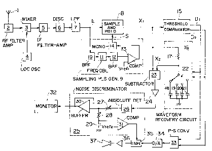
Referring to Fig. 1, there is shown a digital radio
receiver including a noise detection circui'c of the present
invention. The radio receiver is adapted to receive a
radio-frequency signal from a transmitter station in which
the original baseband signal is a binary digital signal
which is frequency modulated upon plural carriers having
four different frequencies or phase modulated upon a single
carrier into a quarternary phase shift keying (PSK) signal.
For porposes of error rate reduction, the baseband signal is
converted to an error-immune coded format prior to the
modulation in a manner well known in the art. The radio
receiver includes the antenna 1 which intercepts the RF
signal and drives a radio-frequency filter/amplifier 2 whose
output is connected to an input of a mixer 3 to which the
output of a local oscillator 4 is also applied. The output
of mixer 3 drives an intermediate frequency filter/amplifier
5, which in turn drives a discriminator, or angular
demodulator 6 to generate a signal as a replica of the
original baseband signal. For purposes of disclosure, it is
assumed that the transmitted signal is frequency modulated,
and so the the angular demodulator is a frequency
demodulator. The modulated baseband signal is applied
through a Nyquist lowpass filter 7 to produce a waveform E
which is applied to a sample-and-hold circuit 8 and a
sampling pulse generator 9.
1306~
NE- 9 4 -MK
( 008A/M4 )
Sampling pulse generator 9 is formed by a bandpass
filter 10, a frequeny doubler 11 and a bandpass filter 12.
Bandpass filter 10 has a center fre~uency corresponding to
one half of the symbol rate of the received signal and
bandpass filter 12 has a center frequency corresponding to
the symbol rate. The frequency of the output of the
bandpass filter 10 is doubled by frequency doubler 11 and
passed through the bandpass filter 12 to a comparator 13 for
comparison with a reference voltage Vrefl. When this
reference voltage is reached, the comparator 13 drives a
monostable multivibrator 14 to produce a narrow sampling
pulse S. As illustrated in Fig. 2a, the four-level digital
signal has an eye pattern having eye openings formed by
waveforms El, E2, E3 and E4 of the received signal E. As is
well known in the art, the eye pattern is a trace of the bit
stream on an oscilloscope which is set to trigger on the bit
rate with a sweep duration of a unit bit interval, and the
eye openings decrease with additive noise and bandwidth
limitations. The best time t~ sample the received signal is
when the eye openings are largest. Sampling pulse S (Fig.
2b) is generated so that it coincides with the timing at
which the eye openings are largest. Sample-and-hold 8
responds to the sampling pulse by sampling and holding the
input waveform E to produce an output signal Xl which forms
an eye pattern as shown in Fig. 2c. As indicated, the
sampled signal Xl assumes one of four voltage levels vll,
v12, v13 and v14 which correspond respectively to the
waveforms El, E2, E3 and E4. If the received signal is
contaminated with noise, the sampled voltages appear as
30 closely spaced parallel horizontal lines.
The output signal Xl of sample-and-hold 8 is applied
to a threshold comparator 15. Threshold comparator 15
essentially comprises four comparators having decision
1306~()4
NE-94-MK
(008~/M4)
-- 5
thesholds Vl, V2, V3 and V4 corresponding respectively to
the crossover points of the waveforms El, E2, E3 and E4 when
the center frequency of the output of mixer 3 is aligned
with the center frequency of the IF filter/amplifier 5.
Each comparator generates an output signal when the input
waveform exceeds its decision threshold. The outputs of the
comparators are connected to a logic circuit to convert them
into a pair of binary signals Dl and D2 such that they
assume one of combinations tl, 1), (1, 0), (0, 1) and (0, 0)
corresponding to the reference voltages Vl, V2, V3 and V4,
respectively. Figs. 2d and 2e illustrate the eye patterns
of the binary signals Dl and D2, respectively.
The binary outputs of threshold comparator 15 drive a
waveform recovery circuit 16 which comprises a resistor 17
connected at one end to the output of sample-and-hold 8, and
a plurality of storage capacitors 18, 19, 20 and 21 of equal
capacitance values. Each of the capacitors 18 to 21 has one
end coupled to ground and the other end coupled respectively
to terminals of a high speed electronic switch 22 which may
be implemented by semiconductor analog gates. Electronic
switch 22 is responsive to the binary signals Dl and D2 to
selectively establish a switched connection between resistor
17 and a selected one of the storage capacitors 18 to 21 so
that these capacitors respectively store charge packets of
the sampled voltages vll, v12, v13 and v14. Resistor 17 and
each of the switched capacitors 18 to 21 provide a time
constant which is much greater than the time interval
between successive symbols of the received signal. The
storage capacitors 18, 19, 20 and 21 build up charges which
result in voltages v21, v22, v23 and v24, respectively. By
virtue of the random occurrence of noise, voltages v21, v22,
v23 and v24 represent average values of voltages vll, v12,
v13 and v14, respectively, over time. Therefore, the eye
13~iS()4
NE--94--M~
( 008A/M4 )
pattern of a combined voltage X2 developed across the
storage capacitors appears as single horizontal lines
corresponding to voltages v21, v22, v23 and v24 as indicated
in Fig. 2f. As a result, the signal X2 can be considered as
a replica of the original four-level digital signal and the
signal Xl will have the same waveform as the signal X2 if
there is no noise in the received signal. In addition,
since the size of eye openings differs from one system to
another due to manufac~uring tolerances including
transmission and reception modulation indices and
frequencies of the transmitted carrier and receiver's local
oscillator, the averaging effect of the waveform recovery
circuit 16 allows the output signal X2 to assume a uniform
value independent of the manufacturing tolerances.
Signals Xl and X2 are applied to a subtractor 23 to
extract the noise from the signal Xl. As mentioned above,
the output of waveform recovery circuit 16 contains no
undesirable random factors caused by systems's tolerances,
and therefore the output of subtractor 23 is a true
representation of noise including white noise and a noise
impulse introduced from external sources. A further
advantage of the eye pattern sampling and switched capacitor
storage technique of the invention is that it allows
simplification of circuitry.
The extracted noise is amplified by an amplifier 24
and so the eye pattern of the amplified noise appears as
indicated by a waveform X3 in Fig. 2g. The output of
amplifier 24 is applied to a noise discriminator 25 which
comprises an absolute detector 26 to detect the absolute
value of the noise. The output of absolute detector 26 is
coupled by a variable resistor 27 and a buffer amplifier 30
to a monitor circuit 32 on the one hand and coupled by a
13C~6SO~
NE-94-MK
(008A/M4)
series circuit including a variable resistor 28 and a
capacitor 29 to ground on the other. A circuit node between
variable resistor 28 and capacitor 29 is connected to a
comparator 31 which compares the voltage at the circuit node
with a reference voltage Vref2. Comparator 31 generates a
squelch signal when the voltage at the circuit node exceeds
the reference voltage Vref2.
If resistor 27 is adjusted to a value much lower than
that of resistor 28, the output of buffer amplifier 30
represents the instantaneous value of the noise more
accurately than the average value of the noise. Whereas, if
resistor 27 is adjusted to a value much higher than that of
resistor 28, the output of buffer amplifier 30 represents
the average value of the noise more accurately than the
instantaneous value. If variable resistors 27 and 28 are
adjusted equal to each other, the buffer amplifier 30
produces a high voltage DC output when the field strength of
the received signal is low and produces an impulsive output
when a noise impulse is introduced to the signal.
The binary outputs of threshold comparator 15 are
further applied to a parallel-to-serial converter 33 where
the parallel outputs Dl and D2 are converted to a sequence
of binary signals and applied to a digital-to-analog
converter 34. A replica of the original analog signal is
thus obtained by the D/A converter 34. The output of D/A
converter 34 is applied to an inhibit gate 35 to the control
terminal of which is connected the output terminal of
comparator 31 to prevent the application of the output of
D/A converter 34 via power amplifier 36 to a loudspeaker 37
when the comparator 31 produces a squelch signal.
Frequency or phase jitter of the received signal is
1306~04
NE-94-MK
(008A/M4) - 8 -
another source of noise since it is translated by the
discriminator 6 into undesired amplitude variations. Since
the four-level digital signal which is the baseband signal
containing a DC component is cancelled by subtractor 23, the
output of subtractor 23 can be utilized to control the
frequency of the local oscillator to compensate for such
time-axis jitter. The advantage of this frequency control
resides in the elimination of the need to employ a lowpass
filter which would be required to reject the DC-containing
baseband signal if the frequency control signal is to be
derived directly from the discriminator 6. Otherwise, such
a lowpass filter would form part of a negative feedback loop
and introduce a substantial amount of delay into the closed
loop, which makes it unsuitable for a radio receiver which
is adapted to receive an RF signal whose baseband is a
digital signal.
Fig. 3 is an illustration of a radio receiver which
includes a variable frequency local oscillator 40. In Fig.
3, parts corresponding to those in Fig. 1 are identified by
the same numerals as used in Fig. 1. The output of
subtractor 23 is applied to a lowpass filter 41 to smooth
the noise extracted by subtractor 23 into a DC voltage,
which is applied through a switch 42 to the control terminal
of local oscillator 40. A negative feedback loop is
therefore formed in the receiver to compensate for time-axis
jitter which may occur in the input signal of the
discriminator 6. If the communication is interrupted and a
no-signal condition exists, a large amplitude voltage would
develop at the output of subtractor 23 and affect the local
oscillator 40 to such an extent that it remains unstable for
a certain period of time following the resumption of
communication. For this reason, the output of lowpass
filter 41 is applied to a comparator 43 for comparison with
~3Q6S()4
NE-94-MK
(008A/M4)
a reference voltage Vref3 which represents a no-signal
condition. Comparator 43 generates an output when the
output of lowpass filter 41 exceeds the reference. To
stabilize the local oscillator 4~, the comparator output is
coupled to the control terminal of switch 42 to apply a
reference, or ground potential to the control input of local
oscillator 40, instead of the output of lowpass filter 41.
The foregoing description shows only preferred
embodiments of the present invention. Various modifications
are apparent to thosè skilled in the art without departing
from the scope of the present invention which is only
limited by the appended claims.