Note : Les descriptions sont présentées dans la langue officielle dans laquelle elles ont été soumises.
~3U7~i3
-- 1 --
'h /Vl C f 7~ J/~c .B
Semiconductor device
The present invention relates to a semiconductor
device, and more particularly to a compound semiconductor
device with a high operating speed, such as a gallium
arsenide transistor.
Gallium arsenide semiconductor devices have been used
for high speed signal processing in a high frequency band
such as a GHz band.
To enable the prior art to be described with the aid
of diagrams, the figures of the drawings will first be
10 listed.
Fig. 1 (a), (b) and (c) are sectional views showing
the structure of a conventional gallium arsenic
semiconductor device,
Figs. 2 and 3 are perspective views showing examples
15 of a semiconductor device according to embodiments of the
present invention,
Fig. 4 is a sectional view showing a center portion of
the semiconductor device shown in Fig. 3, and
Fig. 5 (a) to (d) are sectional views showing each
20 process of manufacturing a semiconductor device according
to the present invention.
As shown in Fig. 1 (a), a gallium arsenide semi-
:13t~'7~ ~3
conductor chip is mounted in a cavity 2 in a centralportion of a base 1 that is made of a ceramic material
such as alumina. Electrodes (not shown) on the chip 3 are
connected to terminals formed in thick film printed
5 circuit patterns 4 on a peripheral portion of the cavity 2
using bonding wires 5 made of gold for example.
However, the surface of the ceramic base 1 is so rough
that it is difficult to form a circuit with high precision.
In order to form circuit patterns on the rough surface of
10 the base, the minimum width of the printed circuit 4 must
be approximately 100 ~m, making it impossible to form the
circuit patterns with high density. A]so, since it is
difficult to form ground conductors for isolation, proper
impedance matching cannot be achieved and the degrees of
15 the freedom of the circuit patterns are few.
Another example of a packaging type of conventional
semiconductor device is shown in Fig. l(b), in which thin
film circuit patterns 12 are formed on the flat upper
surfaee of a ceramie base 11, the patterns 12 being
20 connected by wires 14 to a gallium arsenide semieonductor
ehip 13 whieh ls secured to a eentral portion of the
surfaee of the base 11 by die-bonding.
Even in this ease, however, beeause of using ceramic
material a.s the base 11, the minimurn width oE eaeh of the
25 eireuit pattern.s 12 can be decrea~sed to only up
approximate]y 10 ~m, and integral multilayer Eilm circuit
patterns eannot be formed on the base 11. Therefore, the
arrangement shown in Fig. l(b) is not suitable Eor high
density mounting.
A further example of a paekaging type oE conventional
semieonduetor deviee is shown in Fig. l(c), in which there
is die-bonded a galliurn arsenide semieonductor chip 23 in
a eentral portion of the upper surfaee of a silieon
substrate 21 having thin film eircuit patterns 22 formed
1307~S3
3 --
on its surface. The patterns 22 are connected to the chip
23 by wires 24. In this case, since the flatness of the
surface of the substrate 21 is noticably improved by using
a silicon substrate, the minimum width of the circuit
5 patterns 22 can be approximately 3 ~m.
However, in any of these cases the heat discharging
characteristic of the semiconductor device is inadequate.
A large amount of heat will be generated in the semi-
conductor device during operation at a high frequency of
10 more than 500 MHz, and, since this heat cannot be
sufficiently radiated in the conventional arrangements,
the frequency characteristics of the semiconductor device
are badly effected. Hence these conventional semi-
conductor devices are not suitable for high frequency
15 operation. In addition, any arrangement for improving the
heat radiation characteristics is apt to deteriorate the
packing density of the device.
An object of the present invention is to provide a
semiconductor device that is capable of improving the
20 packing density, with a high heat radiation characteristic
and good operating characteristic at high frequencies,
such as the microwave region.
To this end, the invention consists of a semiconductor
device comprising a metallic base, a silicon substrate
having a circuit formed on or below the surface of the
substrate with a ho]e defined in the central portion oE
the .substrate, a semiconductor chip disposed in the hole
of the silicon substrate and fixed directly to said
metallic base, and circuit patterns formed on the surEace
of the silicon substrate for connecting to the semi-
conductor chip.
The heat generated in the semiconductor chip is
transmitted to the metallic base and can be efEectively
radiated, so that the temperature rise of the chip can be
effectively suppressed. Moreover, thin film circuit
~3~'7i~1 ~3
patterns can be precisely formed in the peripheral portion
of the silicon substrate surrounding the semiconductor
chip, so that the width of these patterns can be decreased
and the package density of the device can be increased.
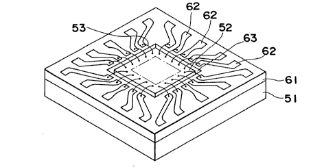
As shown in Fig. 2, a silicon substrate 61 of generally
rectangular shape is secured on the surface of a metallic
base 51 of a copper-tungsten alloy (20% tungsten and 80~
copper, for example) to facilitate heat radiation or heat
dissipation from a semiconductor chip 52 disposed in the
silicon substrate 61. The coefficient of thermal
expansion of the copper-tungsten alloy is 6.9 x 10 9C 1,
which is approximately equal to that of gallium arsenide.
Moreover, since the copper-tungsten alloy has a large
coefficient of thermal conductivity of 2.8 W/cmC, this
alloy is peculiarly suitable for use with a semiconductor
device according to the present invention.
There is a rectangular hole 63 at the central portion
of the substrate 61. A compound semiconductor chip, such
as a gallium arsenide semiconductor chip 52 having an
integrated circuit, is accommodated in this hole 63 and is
directly fixed to the surface of the metallic base 51.
There are a plurality of connecting patterns 62 extending
radially on the surface of the substrate 61 in the
periphera] area around the hole 63. The e]ectrodes (not
.shown) of the chip 52 are connected to the connecting
patterns 62 by wires 53.
Another embodiment of semiconductor device shown in
Figs. 3 and 4 uses a silicon substrate 71 secured on a
metallic base 51 similarly to that shown in Fig. 2. The
silicon substrate 71 comprises a circuit area 72 in which
a multilayer printed circuit is formed for connecting the
terminals of the gallium arsenide semiconductor chip 52 to
electrodes 73 disposed on the surface of the substrate 71
around the peripheral edge portion thereof. A circuit
arrar,gement of passive elements, such as capacitors or
~;~07(~53
-- 5
resistors, or active elements such as transistors, may be
provided in the clrcuit area 72. Provision of such
passive and/or active circuit elements may increase the
kinds of operation of which the semiconductor device is
5 capable. Such a circuit arrangement may be suitable for a
device operating in a low frequency zone.
In this arrangement, since the chip 52 is directly
attached to the metallic base 51, the heat generated in
the chip 52 can be efficiently dissipated through the
10 metallic base 51. Moreover, since it is possible to form
a circuit with high density on the silicon substrate, the
pack density of the circuit can be increased up to the
limit of the wire-bonding.
A process of manufacturing such a semiconductor device
15 will be explained with reference to Fig. 5.
First, there is prepared a silicon substrate 70 whose
surface is a crystal orientation (100) surface having a
connecting circuit (not shown) in a predetermined pattern
~ormed on or below the surface of the substrate 70. Then,
20 a mask layer 81 is formed on the surface of the substrate
70 by patterning, as .shown in Fig. 5(a). Subsequently, a
predeterrnined area of the substrate, corresponding to the
hole portion, is etched with an etchant of a mixed liquid
including ethylenediamine, pyrocatechol and water, whereby
25 a hole 74 with a side wall 74a of crystal orientation
(111) inclined at an angle of 54.7 to the horizontal
surface is formed, as shown in Fig. 5(b). After that, the
silicon substrate 71 is die-bonded onto the metallic base
51 in a known method, as shown in Fig. 5(c).
Subsequently, the gallium arsenide semiconductor chip
52 is disposed in the hole 74 and is die-bonded to the
metallic base 51, as shown in Fig. 5(d). In this example,
since the thickness of the chip 52 is equal to the
thickness of the substrate 71, the levels of the outer
surfaces of the chip 52 and the substrate 71 are coincided,
j7~?~3
.
-- 6 --
thereby facilitating the subsequent wire-bonding work.
Subsequently, the electrodes on the chip 52 are
connected to the circuit patterns 62 on the silicon
substrate 71 by wire-bonding, whereby a semiconductor
5 device can be made.
The present invention is not limited to the above
mentioned embodiments and various modifications can be
made. For example, in the present example, although an
etchant of the ethylenediamine group is used for forming
10 the hole portion, an etchant of the hydrazine group or an
aqueous solution of potassium hydroxide can also be used,
and the material of the mask can be selected among
photo-resist, silicon dioxide and silicon nitride, for
example, in accordance with the materials of the etchant.
Moreover, the material of the metallic base for
dissipating heat is not limited to the copper-tungsten
alloy described in the embodiment, and any material having
a large coefficient of thermal conductivity and a
coefficient of thermal expansion approximating that of
20 gallium arsenic can be used. Moreover, though the circuit
layer oE the silicon substrate is formed on the surface of
the .suhstrate, an integral multi-pack film can also be
Eormed.
Furthermore, the surface of the silicon substrate is
25 not ]imited to a crystal orientation (100), and, if the
surface of the silicon substrate is made to be a crystal
with orientation (110), a hole portion with a side wall
vertical to the horizontal surface can be formed by the
etching process.
As described above in detail, a silicon substrate with
a circuit is ~ixed onto a metallic base for dissipating
heat, and, since a compound semiconductor chip is fixed to
the metallic base for discharging heat in the hole portion
formed in the silicon substrate, the heat generated in the
1 3~ 23
. .
-- 7
chip can be efficiently discharged, and, since it is
possible to form a circuit with high density on the
surface of the silicon substrate, a semiconductor device
having a circuit with high density can be realized.