Note : Les descriptions sont présentées dans la langue officielle dans laquelle elles ont été soumises.
1309503
1 --
Field of the Invention
This invention relates generally to multiple
processor configurations and, more particularly, to
circuitry and associated methodology for enabling each
processor to receive selectively only pertinent portions
of data that is broadcast to the processor over a
communication bus interconnecting the processors.
Backqround of the Invention
A programmable digital computer provides a
readily adaptable environment to simulate physical systems
such as a communication network or a multi-layer protocol.
However, in order to make simulations tractable for
complex systems, oftentimes it is necessary that parallel
processing be utilized. With parallel processing, system
computations are subdivided into tasks that are suitable
for execution in parallel. The tasks are then distributed
among a plurality of synchronized processors for
autonomous execution. Conventionally, computation results
are stored in a single memory which is common to or shared
among the several processors via a multiple access memory
bus interconnecting the memory with the processors.
Traditional methods for accessing and then
storing computational data into the single memory possess
inherent deficiencies. Two prime areas of difficulty are
excessive loading of the memory bus and high overhead
manifested by e~ctra, unproductive processor cycles. Both
of these factors may lead to unsuccessful access to the
memory because of busy or blocking conditions exhibited by
either the bus or the memory, or both simultaneously~ The
main cause of these difficulties is the constraint induced
by the architectural arrangement, namely, the need to
request and then acquire two shared resources in series
with some probability that access to each resource may
fail. In the case of a failure because of a busy
condition, the entire access process must be continually
repeated until access succeeds. Tha failure rate is
exacerbated whenever the demand for memory access
~3~9~3
increases.
A so-called conflict, that is, a simultaneous update
of the same memory location by two or more processors, is another
situation that is difficult to handle in shared memory systems.
Multiple processors sharing the same data are called overlapping
processes and the prevention of other processors from accessing
shared data while one processor is doing so is called mutual
exclusion. Several conventional techniques for implementing
mutual exclusion, such as semaphores and test and set
instructions, ar~ detailed in the text entitled An Introduction
to Operating Systems, by H.M. Ditel, Addison-Wesley, 19~3,
Chapter 4. These techniques also suffer from similar performance
and overhead problems discussed above and, moreover, are
extremely error-prone when handled by user-written software.
Finally, standard shared memory systems employ a
destructive write process. Thus, when a memory location is
modified, the contents of that location are replaced with the
modified data and the original data is destroyed. This process,
when combined with traditional conflict resolution techniques,
basically obliterates the data history of each memory location,
thereby either limiting the processor to using only the single
data value presently stored in the memory location at the end of
each computational phase or requiring elaborate recompu$ation
procedures to reconstruct overwritten data.
Summary of the Invention
The above-identified shortcomings and limitations of
the conventional methods and associated circuitry for storing
data propagating on a bus interconnecting the processors in a
multiple processor system are obviated, in accordance with the
present invention, by providing each autonomous processor with
an arrangement to receive selectively only pertinent segments of
data propagating over the bus. Illustratively, this is achieved
by providing each processor with both buffer memory means and
means for selectively enabling the buffer means to accept data
on a first-in, first-out basis off the bus. The means for
enabling stores information which is indicative of those segments
of the data that are required by the associated processor. In
B
~L3~03
addition, all of the processors are interconnected with a pending
line which controls the processors as they move progressively
from processing state-to-processing state. The processors are
inhibited from advancing to the next processing state by
assertion of the pending line whenever any processor has state
data to transmit. All processors are released only after all
processors having state data to transmit have completed their
transmission of data; release is initiated by de-asserting the
pending line.
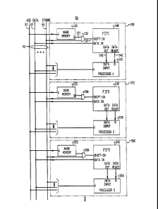
Brief Description of the Drawing
FIG. 1 is a block diagram depicting three processors,
and their associated shared address space circuits, from a
multiple processor system configured in accordance with one
aspect of the present invention;
FIG. 2 depicts, in block diagram form, one processor
and its associated shared address space circuitry from FIG. 1,
wherein the circuitry is shown to further comprise a control
arrangement for conflict resolution and flow control; and
FIG. 3 is a timing diagram for the embodiment in
accordance with FIGS. 1 and 2.
In the FIGS., reference numerals of like elements are
incremented by 100, 200 and so forth depending upon the
particular processor under consideration in the multiple
processor system.
Detailed Description
With reference to FIG. 1, three autonomous processing
entities 100, 200 and 300 in a multiple processor system 50 are
interconnected via common communication bus 60, which is
illustratively the VME-type bus well-known in the computer art.
All other processing entities not shown are connected to bus 60
in the same multiple-access manner.
Each processing unit 100, 200 or 300 includes
130~5~3
stand-alone processors 110, ~10 or 310, and each of these
processors is coupled to shared address space circuitry.
With reference to processor 110, for example, mask
memory 120, first-in, first-out (FIFO) buffer 140 and AND
5 gate 130 are circuits comprising the shared address space
circuitry of processor 110.
Moreover, memory 120, gate 130 and FIF0 140 each
are coupled to bus 60. In particular, memory 120 is
coupled to parallel address (ADD) sub-bus 61, whereas gate
10 130 is connected to STROE~E lead 63 and FIFO 140 has
parallel DATA sub-bus 62 as input. All other shared
address space circuitry associated with the remaining
processors are configured in essentially the same manner.
In addition, each processor 110, 210 and 310
15 operates in essentially an autonomous mode, that is, in
the sense that each processor is composed of an internal
clock (not shown) which is independent of the clocks in
all other processors. Although the processors operate
autonomously, the processors form a parallel processing
20 system having a need to interact such as, for example, by
transmitting information generated by or stored in one
processor to certain other processors requiring that
information; computational data from executed tasks is one
form of the information requiring transmission. This is
25 effected over bus 60 in the conventional manner; for the
VME-type arrangement, an interrupt signal is the indicator
of a transmit ready condition for the broadcasting of
information by one or more processors.
Broadly, as is indicated in FIG. 1, a separate
30 copy of the data broadcast over bus 62 may be stored by
FIFO's 140, 240 and 340. When data is written on bus 62,
the data is registered simultaneously in each enabled
FIFO. Hence, in contrast to the conventional single
memory implementation, the arrangement in accordance with
35 the present invention utilizes replicated, distributed
FIFO buffers that are selectively enabled to receive data
on bus 62. This makes it possible for each processor to
1309~0'~
-- 5 --
accept only the data that is pertinent to its tasks from
what is broadcast over bus 62. Once copied, reading of
the data by any particular processor 110, 210 or 310 may
occur asynchronously from its associated private copy
In particular, by way of a combined circuit and
operational description, the arrangement exemplified by
processing unit 100 is now considered. Other processing
units behave similarly. Mask memory 120 is illustratively
a one bit wide memory having its address input (A)
connected to bus 61. Memory 120 stores an enable bit at
each address which is pertinent to its associated
processor 110. The output (Q) of memory 120 serves as one
input to AND gate 130 via lead 121. The other input to
gate 130 is STROBE lead 63 of bus 60. The STROBE signal
indicates when data is stabilized and may be read off
bus 60. The output of gate 130, on lead 131, serves to
enable the SHIFT-IN input of FIFO 140. With this coupling
arrangement, the one bit of mask memory 120, when ANDed
with the STROsE signal, allows FIFO 140 to receive
selectively the data presented to its DATA IN port. Since
a given processor usually requires only a limited portion
of the broadcast data, the AND operation effectively
filters unwanted data under control of the contents of
memory 120. Moreover, this arrangement of FIFO 140
effects non-destruct write operations. Since every data
update is stored when received on a first-in, first-out
basis, processor 110 has available a history of variable
changes. For instance, it is supposed that there are two
successive writes to an enabled memory location by
processing units 200 and 300, respectively. Because of
interposed FIFO 140, the two data segments are stacked in
FIFO 140. Now, if a conflict is detected (as discussed
shortly), the fact that successive segments of data have
been written to the same address and, consequently, are
stored serially in FIFO 140, allows for conflict
resolution according to an algorithm that is appropriate
to the process being executed.
1309~03
-- 6
In discussing conflict resolution, reference is
made to FIG. 2. In FIG. 2, processor 110 and its
associated shared address space circuitry are shown
together with circuitry to control conflict resolution and
flow control. Conflicts are detected by supplying
"PENDING" lead 72 and connecting lead 72 to all processors
of processor system 50. Lead 72 is arranged to have a
"wired OR" characteristic, that is, one or more processors
can force PENDING to its dominant or asserted state. In
FIG. 2, the PENDING signal is transmitted from the P-OUT
port of processor 110 via inverter 154, and PENDING is
received at the P-IN port via inverter 156. PENDIN5 is
asserted by any processor 110, 210 or 310 at the start of
a standard contention cycle on bus 60, and PENDING is
released upon the release of bus 60 after the update
process is complete. If multiple processors are queued
and waiting to use bus 60, PENDING is asserted from the
beginning of the first bus request until the completion of
the last update; FIG. 3, discussed below, presents timing
information.
By way of an illustrative operational
description, the simple case of two processors both
scheduled to modify the same variable simultaneously is
considered. Both processors assert PENDING and contend
for bus 60. The processor that gains control of bus 60
through a standard bus contention mechanism then transmits
its data. The receiving processor receives an interrupt
from its associated FIFO and proceeds to process the data.
This occurs since an interrupt is issued by any FIFO
whenever data is entered. Thus, in FIG. 2, FIFO 140
issues an interrupt signal on lead 142 via the DATA READY
port whenever data is entered into FIFO 140. Upon
completion of processing by receiving processor 110, it
checks the state of lead 72. This lead is still in the
asserted state since the second processor has data to
transmit. Receiving processor 110 remains in the receive
mode until PENDING is cleared after completion of the next
13~9~03
data transmission. Finally, when lead 72 is unasserted,
the receiving processor may begin an appropriate conflict
resolution routine, being assured that all possible
conflicting data has been received. The conflict
resolution scheme, since it is not hard-wired, may be
implemented as appropriate to each simulation application.
For instance, one resolution scheme may deal with the
conflict by taking the first update and discarding all
others; another scheme may be to average the data.
In an~ simulation wherein the FIFO buffers may
be filled at a faster rate than they are emptied, a flow
control mechanism is provided to preclude FIFO overflow.
The FIFO's are configured to provide a signal on their
FLOW port (FIG. 2) whenever they are filled to a
predetermined threshold. The FLOW port is connected to
FLOW lead 71 via, for example, inverter 150 for FIFO 140.
In turn, lead 71 connects to all other processors via, for
example, the F port through inverter 152. Lead 71 is also
arranged to have a "wired OR" characteristic. Whenever
any FLOW port is asserted/ all processors receive an
interrupt through the F port. With lead 71 asserted, the
current transmission is completed and then all processors
process the contents of their associated FIFOs before
allowing additional data input.
To exemplify the timing required of the various
components comprising processing system 50, FIG. 3 is
considered. It is presumed that processors 210 and 310
are propagating ~ariable changes to processor 110
simultaneously. on line (i) of FIG. 3, bus 60 transmits
an INITIATE transfer of data signal to processors 210 and
310. This is shown as TIME POSITION 1 and line (i). Both
processors 210 and 310 assert PENDING on lead 72, as shown
as TIME POSITION 2 on line (ii); also, these processors
request use of bus 60 in order to transmit their data
information. If it is assumed that processor 210 acquires
bus 60 first, then processor 210 begins to transmit its
data; this is depicted as beginning at TIME POSITION 3 on
1309~03
-- 8
line (iii). The data is received by processor 110 through
its shared address space circuitry; in particular, since
FIFO 140 receives data, an INTERRUPT is issued to
processor 110 via the DATA READY port of FIFO 140. This
INTERR~P~ signal is shown as commencing at TIME POSITION 4
of line (v~. In response to the INTERR~PT signal,
processor 110 begins to read the data. TIME POSITION 5 on
line (Yi) depicts the start of the read phase. At TIME
POSITION 6 on line (iii), processor 210 has completed its
write operation. As then indicated by TIME POSITION 7 on
line (vi), processor 110 completes its read phase and
checks the PENDING lead. Since it is still asserted by
processor 310, processor 110 awaits more data. Processor
310 now acquires bus 60 and may begin to write the data
onto bus 60; TIME POSITION 3 on line (iv) indicates the
time that processor 310 begins data transmission. When
data transmission is complete, PENDING is unasserted, as
per TIME POSITION 9 on line (ii). When data processor 110
detects that PENDING is released, it may begin to process
the total data now in its local storage. ~TIME POSITION 10
on line (vii) depicts the start of the processing by
processor 110 and TIME POSITION 11 shows the completion
time. Processors 110, 210 and 310 are now prepared to
proceed with the next phase in the simulation process.
It is to be understood that the above-identified
arrangements are simply illustrative of the application of
the principles in accordance with the present invention.
Other arrangements may be readily devised by those skilled
in the art which embody the principles of the present
invention and fall within its spirit and scope. Thus, for
example, it is possible to configure each shared address
space circuitry (e.g., elements 120, 130 and 140 of FIG.
1) so that an address translation may be effected between
addresses on bus 60 and local memory in processor 110. In
this situation, mask memory 120 is an N+1 bit wide memory
wherein one of the bits is used in conjunction with gate
130 for activating data copying and the remaining N bits
D _~
~309~
g
indicate the address in local memory allocated to store
the data.
Also, whereas the contents of mask memory 120 as
described are static, it is possible to alter dynamically
its contents by also arranging memory 120 with an enable
input so as to receive data off bus 60 to alter its
contents.
Therefore, it is to be further understood that
the circuitry and methodology described herein is not
limited to specific forms disclosed by way of
illustration, but may assume other embodiments limited
only by the scope of the appended claims.