Note : Les descriptions sont présentées dans la langue officielle dans laquelle elles ont été soumises.
~ 3~0~
QUANTIT~TIVE LENSE AN~LYSIS TEC~INIQUE
Background of the Invention
This invention relates generally to a method
and apparatus for quantitatively determining various
characteristics of lense or optical systems1 and more
particularly to a method and apparatus for quantitatively
determining such characteristics of a lense or optical
system as focal position, focus surface or curvature of
the system~ and relative depth of focus throughout the
field of the system. The method and apparatus are
particularly useful in optical systems used in photo
microlithography for the production of semiconductor
integrated circuit chips and wafers, although the use is
not so limited to these systems.
In photo microlithography, a lense system is
used in conjunction with a reticle or mask having the
desired object pattern formed thereon corresponding to
the object pattern which is to be exposed on the wafer
surface. In some cases a single object pattern is
utilized to imagewise expose the entire wafer, whereas in
other cases a step and repeat technique is utilized to
imagewise expose the wafer in successive steps. In
either case, it is necessary to have the entire image as
precisely in focus as possible on the wafer in order to
achieve acceptable line patterns which will be properly
developed and crisply delineated by subsequent
development processing techniques.
As smaller and smaller line sizes are being
used, the criticality of accurate focusing of the optical
system increases. The requirement of accurate focusing
is compounded by the fact the optimal focal position and
the depth of focus of various positions or areas of the
lense or optical system may vary with respect to other
~U~-~7-024
~3102~
positions or areas thus further complicating the task of
trying to obtain optimum focal distance of the wafer from
the lense or optical system. It thus becomes
increasingly critical to precisely determine these
characteristics at various positions or ]ocations on the
lense or optical system. Even further complicating the
task is the necessity to test or i'characterize" the lense
system after it is installed as a part of the
microlithographic system as a whole thus limiting the
nature of test tools tha~ can be used.
In the past, the focal position or "optimum
focal distance" in this type of system has generally been
determined by qualitative evaluations performed by
trained technicians. While the precise techniques vary
slightly they involve a trained operator looking at a
series of lines, or other shapes exposed at various focal
distances to determine which images appear to be the
"sharpest" or "clearest." These images are taken at
various locations on the optical system, and by
repeatedly looking at and qualitatively evaluating such
images, the technicians "decide" which images are the
best, according to their judgement. One variation of
such a technique is described in "Research Disclosures,"
April, 1986, Number 264, Disclosure Number 26,433,
published by Kenneth Mason Publications, Ltd., England.
For certain types of lense systems, forms of
quantative evaluation have been suggested; e.g. in U.S.
Patent 4,435,079, dated March 6, 1984, and entitled
- "Apparatus for Testing Lenses by Determining Best Focus,"
a system is described wherein the intensity of PIXEL
signals is measured at various locatons and focal
distances of a lense and those exceeding a certain
magnitude are counted. This gives an indication of best
focus, but has several drawbacks. First, expensive
BIJ9 87-024
~3~ ~2~:3
precision equipment is required, having
complicatedelectronic circuits. Because of this and
other factors, it is not suited to tesk a lense system in
place in a lense system for a photolithographic tool.
Another tool for evaluating lenses using photo diodes is
shown in U.S. Patent 4,585,3ll~, dated April 29, 1986,
entitled "System for Real-Time Monitoring the
Characteristics, Variations and Alignment Errors of
Lithography Structures." This also requires specialiæed
equipment and gauges to determine received radiation.
Summary of the Present _nvention
According to the present invention, a method
and apparatus are provided for determining the best focal
position of any given location within the exposure field
Of an optical system, and preferably also for determining
the focus surface or curvature of the optical system, and
the relative depth of focus throughout the field. The
invention utiizes a test vehicle having at least one
object group having a large object and a small object,
the small object having a size approximating the
resolution limit of the optical system and the large
object being significantly larger than said resolution
limit~ Preferably there is an array of object groups at
spaced locations on the test vehicle corresponding to
various locations of the optical system to be measured,
the object groups being separated by substantial opaque
regions. The test vehicle is set at a selected distance
from an image snesor so as to allow the large image for
each group to be sensed but not the small image.
Thereafter, the image sensor is moved orthogonally with
BU9-87-02~
~ 3 ~
respect to the optical system and the focus distance of
the optical system is changed and the image groups are
again projected onto the image sensor.The orthogonal
movement, the focus distance change and projecting steps
are repeated successively until the large object and the
small object of each group are sensed as images on the
image sensor, and the orthogonal movements, change of
focus and projecting steps are further repeated
successively until only the large object of each group is
sensed as an image and not the smaller object on the
image sensor. This will produce a series of large object
images and a series of small object images less in number
than the series of large object images. The focal
distance at the median point of the image series
containing the small object image at each location
represents the best focal position of that location of
the optical system, and the number of small object images
in any given series of small object images with respect
to the number of small object images in any other small
object image series represents the relative depth of
focus therebetween.
Description of the Drawings
Figure 1 is a plan view of a test vehicle (not
to scale) according to the invention;
25Figure la is a detail view on an enlarged scale
of one object group on the test vehicle;
Figure 2 is a representation (not to scale) of
a series of imges made from the test vehicle of Figure 1
according to this invention;
30Figure 2a is a detail view on an enlarged scale
of one series of images shown in Figure 2;
~U9-~7~024
~ 3 ~
Figure 3 is a three-dimensional graphic
reproduction of the focus surface o~ an optical system
plotted from data derived from the image of Figure 2;
Figure 4 is a topographical plot of the focus
depth variation plotted from date derived from the image
of Figure 2; and
Figure 5 is a plan view of a wafer, showing in
broken outline the approximate exposure area when the
wafer is used as a sensor.
Description of the Preferred Embodiment
_ __.__
Referring now to the drawings, and for the
present to Figure 1, a test vehicle for characterizing a
lense or optical system on a step and repeat
micorlithography tool according to this invention is
shown. While the invention finds uses in other optical
systems, it is particularly adapted for use in step and
repeat microlithographic tools such as a model 6000
manufactured by GCA Corp. In these tools 9 a mask or
reticle is provided which has the desired pattern formed
thereon which pattern is to be exposed on the wafer
surface which has been coated with photo resist. The
pattern is exposed onto a portion of the surface of the
wafer through a lense or optical system, which reduces
the pattern to the desired size. The wafer is then moved
incrementally and another portion of the surface is
exposed. This "step and repeat" is continued until the
entire surface of the wafer has been exposed, after which
the wafer surface is developed and processed in a
conventional manner.
BU9-87-02~
6~ 3
In this type of tool, it is necessary to have
quite a precisely focused pattern on the wafer surface to
provide satisfactory results, and to this end it is
necessary to very carefully characterize the lense or
optical system. In characterizing the lense or optical
system, it is necessary to determine several parameters,
one of the most important of which is the focal position,
i.e. optimum or "best" focal position, of various
locations in the field of the lense. This is necessar~
since even in the most precise optical system there is
some variation of best focal position at various
locations within the exposure field, the largest
variations normally occurring around the edges or
periphery of the field. It is also desirable to
determine the relative depth of focus of various
positions or areas of the field as well as the focus
surface or curvature of the lense or optical system. The
use of the test vehicle in conjunction with a wafer as an
image sensor according to this invention allo~s the
characterization of a lense or optical system as to focal
position of various locations of the field as well as
determining relative depth of focus of various locations
within the field, and a determination of the focus
surface or curvature of the field.
The test vehicle comprises an array of object
groups, each group comprised of a large object 10 and a
small object 12. The objects are actually openings in an
opaque film such as a chrome layer on a glass plate which
allow transmission of light or other energy therethrough.
The object groups are separated from each other by
substantial opaque regions. The object groups are also
arranged in a pattern such that when the test vehicle is
inserted into the path of the optical system, the image
groups are located at different positions of the field
BU9-87-024
~3~2~
such that they intercept not only the center of the lense
or optlcal system, but also the intermediate and edge
portions of the field. The small objects 12 which
preferably are symmetrical have a dimension that is about
equal to the resolution limit of the lense or optical
system, and the large objects 10, which are preferably
rectangles, have their smallest dimension significantly
larger than the resolution limit of the lense or optical
system. The resolution limit of microlithography tools
is normally defined as that size which when exposed and
developed will provide clear, sharp images in which all
developed material will be removed. However, a size
slightly smaller may actually be sensed and developed at
least enough to be visually observable under a microscope.
Hence, the term resolution limit as used herein is
intended to include a size which can be visibly observed
upon development, which may be slightly smaller than the
rated resolution limit of the tool. Current
microlithography tools, such as the GCA Model 6000,
typically have a rated resolution limit of about 1.0
micron but an object as small as .8 micron can develop
enough to be visually observed. Hence, the smaller
object 12 should be about .8 micron square. The large
object 10 can optimally be about 5x1.2 microns in size
for the purpose of practicing this invention.
To utilize the test vehicle according to the
invention, the test vehicle is inserted in to
microlithography machine in the position where the
reticle or mask residesO A conventional wafer of the
type shown in Figure 5, having been conventionally
prepared with photo resist is located at its normal
position in the tool. Any one of a number of photo
; resist materials can be used, depending upon many factors
BU9 87-02~
including the light source, and light intensity. One
particularly useful resist is AZ1350J, manufactured by
Shipley Corp. The nominal focal distance of the tool is
determined. This will normally be defined by the
manufacturer, or can be calculated from the parameters of
the optical or lense system, or can be roughly determined
by routine experimentation. A typical optimum focal
length for a GCA 6000 series machine is about 251 unitsO
(Each unit is equal to 1/4 micron.) If this were exactly
accurate for the entire surface of the lense or optical
system and the focus system stable, then one could always
use this setting and the best focus would be obtained.
However, due to inherent variations within the exposure
field and the instability of the focus system, the actual
best focus for various locations on the lense or optical
system may differ, and that is what this invention
determines. To make this determinakion, the nominal or
published best focus of the lense or optical system is
determined. This is normally published by the
manufacturer. However, if for some reason it is not
available, it can be established by conventional
techniques of repeated exposure and developing of objects
having a size near the focal resolution limit of the
lense or optical system changing the focal lengths by
incremental amounts until an image is resolved. This is
a well known technique.
Once the nominal focal length of the lense or
optical system is determined, the focal length is changed
(either shortened or lengthened) by a selected number of
units on a tool. For example, on the GCA ~odel 6000, an
initial change of an increase of 14 units is
conventionally usedO A portion of the wafer,
corresponding to the size shown in broken outline in
Figure ~, is then exposed through the test vehicle. The
BU9-~7-02~
131~2~ ~
wafer is then moved orthogonally a very small distance.
This distance should be about 2 times the dimension of
the large object. This movement is not to be confused
with the gross movement for step and repeat exposure in
production of wa~ers, but is of a much sma]ler nature.
The focal distance is then decreased. A typical change
in focal distance is 0.25 micron. The wafer is then
exposed again through the test vehicle. The wafer again
is moved orthogonally, the focal distance clecreased by
0.25 micron, and the wafer exposed again. This movement
and change of focal distance is repeated a number of
times each time the wafer is moved, and the focal
distance shortened. Typically 13 to 15 exposures are
made. If this step and expose sequence is followed, and
fifteen exposures are made, the focal distance of the
lense or optical system will have moved from 1.75 microns
out of nominal best focus on one side through nominal
best focus to 1.75 microns out of nominal best focus on
the other side.
After all the exposures have been made, the
photo resist on the wafer is developed in a conventional
manner. (Shipley*AZ2401 is a good developer for AZ1350J
resist). At the location of each object group a seriesof
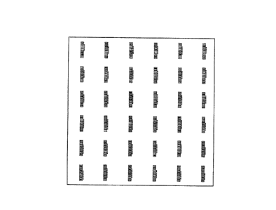
images will be developed as shown in Figure 2 containing
both large object images 1~ and small object images 16.
(These are permanent images that can be preserved and
studied under a microscope.) These im-~ges will appear at
each location as a series of large images 14, with a
corresponding set small images juxtaposed with respect to
some of the large images. The reason that all of the
large object images are developed, but only some of the
small object images are developed9 is that the large
objects can be resolved by the lense or optical system
and sensed on the wafer through a relatively large range
* Trade Mark
BU9-87-02~ ~`
~3~L~2~
of focal distances, whereas the smaller objects, which
are close to the resolution limit of the lense or optical
system can be resolved and printed on the wafer through a
very small range of focal distances. ~ence, at least one
large object is resolved at the start of the sequence
where a small object is not resolved, the sequence
continues wherein both large and small objects are
resolved, to a point when again only the large objects
and not the small objects are resolved. The function of
the large objects is to define the exact setting wherein
the exposure started. If only small objects were used,
one could not tell at which focal distance the objects
were first resolved. Other techniques for identifying
which small objects are resolved without the use of a
large object are also possible. For example, the small
objects could be exposed in some definitive pattrn, such
as a circle such that any 2 or more small objects
resolved would have a unique relationhip to each other,
and thus identify where in the sequence of exposures they
occurred.
One of the benefits of the present invention
over prior art techniques is that with this invention the
entire series of images at each given location of the
exposure field can be viewed simultaneously, and the
count made. with prior art techniques, each expsoure of
the object pattern has to be viewed separately, so the
operator does not have a series of exposed object images
in view simultaneously, but must view them serriatum, and
try to remember their characteristics from one view to
another and make subjective judgemental comparisons.
The best focus distance for the locations on
the lense or optical system represented by each series of
images is the mid-point, or median point, of the series
of small object images. ~s can be seen in Figure 2a, the
BU9-87-02~
~3~2~
11
best focus setting for the location represented by that
series of images is 240 units on the instrument scale;
i.e. four small objects were resolved at settings closer
than 240 units, and four small objects were resolved at
settings greater than 240 units. Hence there is no
qualitative judgement or comparison required by an
operator. The operator or technician doing the
evaluation need only count the number of small objects
resolved on the wafer at each location and the mid point
of the number represents the best focus for that location.
As can be seen in Figure 2, the best focus position of 36
different locations on a lense system can be determined
utilizing this particular test vehicle. This information
can be graphed then to show the focus surface or
curvature of the lense or optical system as shown in
Figure 3. Another advantage of the technique according
to this invention over that of the prior art, is that the
entire method is carried out within a very small area of
the wafer (as shown in Figure 5), rather than over the
entire wafer surface; and the less area involved, the
less chance there is of wafer surface and resist film
variations.
The series of images also can be used to
determine the relative depth of focus variation of the
exposure field at the various locations. The relativ~e
depth of focus of any location with respect to any other
is the ratio between the number of small object images
resolved at one location with respect to the number of
small object images resolved at the other locaiton. Thus
the relative depth of focus of a locaiton in which 7
small object images are resolved to that where 8 small
object images are resolved is 7/8 or o875~ A graph of
focus depth variation of the lense system based on the
resolution shown in Figure 2 is shown in Figure 4. In
BUp~87-02~
12
this Figure, a topographical "map is shown representing
those positions in the field where 6, 7, 8, and 9 small
objects are resolved.
If it should happen that when the wafer is
developed after 15 exposures as described above, there
are some series where only large object images are not
resolved on both sides of where large and small object
images are resolved, the process can be repeated with
some adjustments. It may be sufficient to change the
starting point distance of the lense or optical system
from the wafer, based on the patterns of images, or it
may be necessary to either increase the incremental
changes in f`ocal length or add to the number of exposures
in the series. In any event, minor e~perimentation will
yield a series of object images patterns which can be
used to quantitatively determine best focus position of
various locations of a lense or optical system, as well
as determining the relative depth of focus of the
positions and to determine the focus surface or curavture
of the lense or optical system.
While the invention has been described using 36
object groups, more or less can be used as needed. In
fact, just a single object group in some cases may be
sufficient if only one location is characterized.
BU9~87-02~