Note : Les descriptions sont présentées dans la langue officielle dans laquelle elles ont été soumises.
``` ~3~3~
Ti~le of the Invention:
INFORMATION ~ARD WITH PRINTED BAT~ERY
Field of the Invention:
The present invention relates to a thin
electronic device having an integrated circuit chip and
a power battery for supplying electric power to the
integrated circuit chip, as well as a method for
producing same~
Descrip~ion of the Prior Art:
~ ecently, with the tendency to thinning of
~mall-sized electronic devices, there have been
developed card-type electronic calculators having an
integrated circuit chip between resin sheets and a power
battexy for supplying electric power to the integrated
circuit chip, as well a thin electronic devices such as
IC card having a memory functil)n.
Heretofore, a button- ox coin-shaped battery
has been used in small-sized electronic devices. The
thickness of such thin electronic devices is defined to
be a maximum of 0.80 mm by JIS. But the use of a
~k
~. ~
button- or coin-shaped battery in a thin electronic
device has heretofore made it difficult to fabricate the
electronic device within the said rated value of
thickness.
Recently, moreover, applications of such IC
card have been considered, for example, to a theft
detecting system or an automatic goods sorting system,
as disclosed in Japanese Patent Publication No.
22997/84. However, since it is necessary to use a large
number of IC cards as consumables, there has arisen the
necessity of mass-producing IC cards inexpensively.
According to the prior art, the body of a thin
electronic device and a battery are produced separately
and thereafter the battery is inserted into the body.
This method, however, is very troublesome and poor in
productivity, leading to increase of cost.
Summary and Object of the Invention:
Accordingly, it is one object to provide a
card-type elçctronic device and its manufacturing method
which overcomes the above-described disadvantage.
It is another object to provide a card-type
electronic device and its manufacturing method which
enables the device to be thinner than the conventional
- ~ 31~3~
one.
It is still another object to provide a card-
type electronic device and its manufacturing method
which makes it easy and low in cost to manufacture the
device.
According to one aspect of the present
invention there is provided a method for producing an
information card, comprising:
a first printing step of forming by printing
an electroconductive pattern and a first electrode
surface of a battery on a first cover sheet;
a first application step of applying a battery
activator onto the first electrode surface;
a resting step of resting an electrolyte-
impregnated separator onto the first electrode surface;
a fixing step of fixing an IC chip to the
electroconductive pattern in a predetermined position;
a second printing step of forming by printing
a second electrode surface of the battery on a second
cover sheet;
a second application step of applying a
battery activator onto the second electrode surface; and
a cutting step of lapping and sticking the
first and the second cover sheet together and cutting
-- 3 --
~ 3 ~ 3 ~l
them into a predetermined size.
According to another aspect of the present
invention there is provided a method for producing an
information card, comprising the steps of:
printing an electroconductive pattern and
first and second electrode surfaces of a battery onto
integrally-formed first and second cover sheet portions;
applying an anodic active material and a
cathodic active material onto the first and second
electrode surfaces, respectively;
fixing an IC chip to the electroconductive
pattern in a predetermined position;
resting an electrolyte-impregnated separator
onto one of the first and second electrode surfaces; and
folding the first and second cover sheet
portions so as to be superposed one upon the other and
cutting them into a predetermined size.
According to a further aspect of the present
invention there is provided a thin electronic device
including:
a first cover sheet with a first electrode
surface of a battery formed thereon;
a second cover sheet with a second electrode
surface of the battery formed thereon;
. : i'
~3~31
an anodic active material applied onto the
first electrode surface;
a cathodic active material applied onto the
second electrode surface;
a separator impregna-ted with electrolyte;
a circuit member positioned between the first
and the second cover sheet and operated by the battery;
and
a connecting conductor formed on the first and
the second cover sheet to connect the first and the
second electrode surface with the circuit member,
the anodic active material and the cathodic `
active material being opposed to each other through the
separator, the first and the second cover sheet being
integrally laminated together to hold the circuit
member.
Brief Description of the Drawings:
Fig. 1 is a schematic explanatory view of a
method for producing an information card according to
the present invenkion;
Figs. 2(a), 2(b) and 2(c) are a plan view, a
sectional side view and a separated side view,
respectively, of the information card;
-- 5 --
3 1
Figs. 3(a) to (g) are plan views of the
information card in the course of manufacturing steps;
Fig. 4 is an enlarged view of an IC chip; and
Figs. 5(a) to (c) are process charts showing
another embodiment of the present invention.
Description of the Preferred Embodiments:
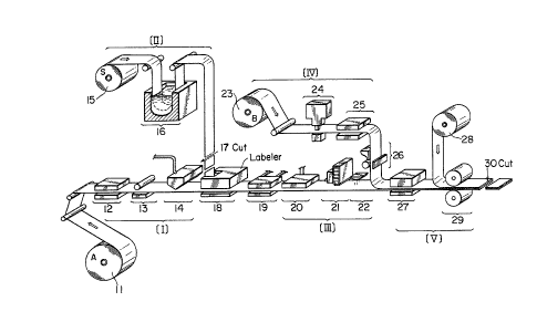
Fig. 1 is a schematic view for explaining the
method for producing an information card accordiny to
the present invention. An example of a concrete
structure of the information card thereby produced is
shown in a plan view of Fig. 2(a), a sectional view of
Fig. 2(b) and a separated side view of Fig. 2(c).
Patterns on the information card surface in
the manufacturing steps of [I] to [V] are shown in
Fig. 3.
For example, as shown in the plan view of
Fig. 2(a) and sectional view of Fig. 2(b), the
information card comprises a back-side cover sheet
(hereinafter referred to also as the first cover sheet)
1 and a surface-side cover sheet (also as the second
cover sheet hereinafter) 2. In the card of this
embodiment, an adhesive sheet 3 is stuck on the upper
surface of the surface-side cover sheet 2 to display the
~3~3~
kind of card.
Between the first and the second cover sheet
there are provided an electroconductive pattern 4, a
flat battery 5 and an IC chip 6, and for thinning
purpose, a hole 2A is formed in the second cover sheet 2
so that tAe IC chip 6 is fitted therein when the first
and the second cover sheet are lapped together.
Part of the electroconductive pattern 4, which
is connected -to the IC chip 6, serves as a pair of
antennas (dipole antenass) 4A2 which change in
characteristic impedance according to the data stored in
the IC memory, while wider area portions thereof serve
as positive and negative electrode surfaces 4Al, 4Bl.
As best seen in Fig. 2(c), the battery 5 is
formed by applying active materials 5A and 5B (Zn, MnO2)
of the battery in the state of gel onto the electrode
surfaces 4Al and 4Bl which are formed by the printing
technique or the like on the first and second cover
sheets 1, 2, and then sandwiching an electrolyte-
impregnated separator 5C in between the cover sheets 1
and 2.
On the outer surface of the first cover sheet
1 there may be formed a magnetic film 7 according to ISO
standards as in ordinary magnetic cards~
~ 3~3~L
An embodiment of the present invention ~or
producing such information card as mentioned above will
be described hereinunder with reference to Fig. 1.
In Fig. 1, the numeral ~1 denotes a band-like
cover sheet (A) formed of pol~ethylene terephthalate
(PET) or polypropylene (P-P) and having a thickness of
about 50 ~m. The cover 11 is drawn out by a roll in the
illustrated direction and fed to a magnetic stripe
printing section, wherein a magnetic film area according
to ISO standards is formed on the lower surface of the
cover sheet ll(A).
Numeral 13 denotes a screen printing section
(A) for forming a wiring pattern on the upper surface of
the cover sheet 11. In the screen printing section 13,
such a wiring pattern as shown in Fig. 3(a) is printed
to the cover sheet 11, using an electroconductive
coating material such as, for example, pasty carbon,
copper which has been made pasty, or pasty mercury.
The portion 4Al of this wiring pattern
represents an electrode surface [4Al in Fig. 2(c)]
serving as a negative (-) pole of the battery in the
information card, while the portion 4A2 represents an
electroconductive surface serving as antenna.
Numeral 14 denotes an active material applying
~ ~ ~ D ~ 3 Jl
section for applying zinc (Zn) gel acting as an
activator in the battery to the portion 4AI which serves
as an electrode surface as in Fig. 3(a), and in the
portion indicated by rightwards oblique lines in Fig.
3(b), Zn gel 5A is applied onto the upper surface of the
wiring pattern 4Al in a thickness of about 50 ~m.
Numeral 15 denotes a separator sheet in the
battery which sheet is formed by kraft paper for
example. The separator sheet 15, which is rolled,
passes through an electrolyte impregnating section 16,
whereby it is impregnated with electrolyte, e.g. ZnCl2.
The thus electrolyte-impregnated separator 5C
is cut into a predetermined size in a cutting section
17, then in a separator sticking section 18 it is placed
on the electrode surface 4Al of the wiring pattern, as
shown in Fig. 3(c).
sy the above continuous steps there is
constituted the first cover sheet 1 (surface A).
Then, in a mask mounting section 19, as shown
in Fig. 3(c), a frame 8 is stuck to the first cover
sheet having the surface A so as to slightly raise the
peripheral portion of the wiring pattern. Further, in a
hardener applying section 20, a small amount of a
hardener 9 is applied to the first cover sheet in a
~3.~3~
position in which the IC chip 6 is to be fixed.
At this time, a polyester-based hot melt
adhesive is screen-printed -to the outer peripheral
portion of the electrode surface 4AI.
Numeral 21 denotes an IC chip packaging
machine. IC chips 6 extruded one by one from the IC
chip packaging machine 21 are each pushed against the
wiring pattern in a predetermined position. For
example, as shown in the enlarged view of Fig. 4, lead
terminals of the IC chip 6 are formed as bumps 6A, which
are pushed against the wiring ~attern 4 in
predetermined positions. Then, infrared ray is
radiated from an infrared ray radiating section 22 to
the pre-applied hardener 9 to thereby fix the firs-t
cover sheet 1 and the IC chip 6 together.
Since the hardener 9 hardens and contracts
upon radiation of infrared ray, the bumps 6A and the
wiring pattern 4 are held in a good electrically
conducted state.
The cover sheet of the surface A shown in
Fig. 3(d) with the IC chip 6, battery active material
and separator formed thereon is then lapped with a
cover sheet 23 which serves as the second cover sheet 2
and both are stuck together.
-- 10 -- ,
~L3~3~
More specifically, the cover sheet (B) IPET or
P-P) 23, which is rolled, is drawn out in the arrowed
direction and fed to a puncher 24, in which there are
formed an aperture sl for IC chip and apertures s2 for
antenna contact, as shown in Fig. 3(e).
The aperture Bl is formed in the position
corresponding to the mounted position of the IC chip
fixed to the cover sheet of the surface A as mentioned
above, while the apertures B2 are formed in the
positions corresponding to the antenna areas (4A2, 4A2).
The cover sheet (s) thus formed with the
apertures Bl and s2 is then fed to a screen printing
section (B) 25, in which an electroconductive wiring
pattern such as that shown in Fig. 3(f) is printed to
the cover sheet.
The greater part of the wiring pattern is in
corresponding relation to the electrode surface (4Al) of
the surface A, forming a positive (+) electrode surface
[4B~ in Fig. 2(c)] of the battery.
Then, in an active material applying section
(B) 26, for example zinc oxide 5s (ZnO2) which is in the
state of gel is applied as a depolarizer to the
electrode surface of the surface B in a thickness of
about 50 ~m to form the cover sheet of Fig. 3(g).
~1 3 ~ 3 ~
Preferably, at this time, a polyester-based
hot melt adhesive is screen-printed also to the outer
peripheral portion of the electrode surface l4Bl).
This cover sheet (B) of the surface B and the
foregoing cover sheet (A) of the surface A are lapped
together and united, for example by h~at-treating -the
two at 130C for about 15 minutes or by an ultrasonic
fusion-bonding technique. At this time, the batter~
electrode surfaces are completely sealed by the ho~ melt
adhesive.
In this case, it goes without saying that both
sheets should be lapped together and united for
registration between the pattern on the surface A and
that on the surface B and in such a position as to
permit the IC chip 6 to be embedded in the aperture B1.
Numeral 28 denotes an adhesive tape, which is
stuck to cover the apertures Bl and B2 of the cover
sheet (B) which has been rendered integral with the
other cover sheet by fusion-bonding for example.
Lastly, the integral sheet member is cut into
a predetermined size (e.g. a size according to ISO
standards) by means of a cutter 30 to obtain such
information card as shown in Fig. 2.
Although in the information card manufacturing
- 12 -
3 ~
method described above the cover sheets (11, 23) of the
surfaces A and B which constitute the information card
are fed separately, there may be used cover sheets (A)
and (s) which are in a united state from the beginning.
More specifically, as shown in Fig. 5(a), a
cover sheet 31 serving as both surfaces A and B has a
groove G which permits folding upwards and downwards
with respect to a central line. The surface of the
cover sheet 31 is divided into surfaces A and B on both
sides of the groove G, and wiring patterns 4A and 4B are
printed on the surfaces A and B, respectively, using an
electroconductive coating material.
As previously noted, Zn gel is applied to an
electrode surface 4Al of the wiring pattern 4A, while
ZnO2 gel is applied to an electrode surface 4B1 of the
surface B. And as shown in Fig. 5(b), a separator 5C
impregnated with electrolyte is put on the surface B,
and apertures Bl and B2 are formed on the same surface.
Further, an IC chip 6 is fixed to the wiring
pattern on the surface A using a hardener as noted
previously and there is formed such cover sheet as shown
in Fig. 5(b). The wiring patterns on the surfaces A and
B of this cover sheet are connected together through an
electroconductive path 4C extending across the groove G.
The cover sheet of Fig. 3(b) is folded along
the groove G as shown in Fig. 3(c), to superpose the
surfaces A and B together to form an information card.
Also in this second embodiment there are used
most of the devices used in the manufacturing method
illustrated in Fig. 1. The secon~ embodiment is
advantageous in that the screen printing sections 13, 25
and the active material applying sections 14, 26 can be
gathered at one place, thus permitting further
simplification of the manufacturing system.
- 14 -