Note : Les descriptions sont présentées dans la langue officielle dans laquelle elles ont été soumises.
1 BACKGROUND OF THE-lNvrN-rIoN ' ~ ) 62
2 1 Field of the Invention
.
3 The invention generally relates to
4 scanning antennas and, in particular, to microwave
landing systems using a signal format which requires
6 multiple antenna functions to provide the signals over
7 wlde coverage sectors.
8 2. Description of the Prior Art
9 Antenna techniques are known which
lû use the phased array scanning beam antenna of a
11 microwave landing system (MLS) to broaden its
12 radiation pattern to satisfy the data antenna
13 requirements. Such techniques generally employ phase
14 spoiling of the phased array aperture. The
fundamental limitation of this technique is that it
16 cannot provide the out-of-coverage indications (OCI)
17 signals and the 360 data signals without employing
18 a single thread multiple port rf switch. This
19 technique is deficient because it is subject to slngle
point failures within the phased array which can cause
21 substantial radiation pattern minima when used in the
22 data antenna mode (low gain - broad pattern). These
23 minima are very difficult, if not practically
24 impossible, to monitor and detect. In addition,
single point system failures also exist and can create
1 3 ~ 2
1 significant sa-~ety risks in certain operational
2 scenarios.
3 The MLS signal format requires multiple
4 antenna functions to provide the signals over wide
coverage sect.ors. The format also provides -for signal
6 transmission outside the normal coveraqe volume, e.g.,
7 out-of-coverage indication signals (ûCI). Inherent
8 growth capabilities in the system such as 360 data
9 link coverage, also require additional antennas in
many practical applications. Because of the multiple
11 antennas required for MLS, an antenna switch is used
12 to connect a transmitter sequentially in time to each
13 antenna port. Although redundant transmitters and
14 control electronics can be enacted on line to provide
signal continuity in the event of a failure, the
16 switching components (rf and logic) are a limiting
17 factor in supporting the requirements for signal
18 continuity in high reliability applications.
19 SUMMARY OF THE INVENTION
It is an object of this invention to
21 provide an MLS employing redundant rf switching of
22 dual signal sources to minimize the effect of switch
23 failures.
24 It is another object of this invention to
provide an MLS system with dual signal sources
--3--
~31~62
1 connected to a primary element array via a passive
2 circulator and switch cornbination which perrnits
3 continued operation even during failure (i.e.
4 fail-operational).
It is ano-ther object of this invention to
6 provide an MLS system with rf and beann steering logic
7 switch arrays for eliminating single point failures.
8 It is another object of this invention to
9 provide a microwave landing system with a recombining
network and switch array for driving auxiliary wide
11 sector antennas with fail-soft performance.
12 The antenna system according to the
13 invention radiates wave energy signals into a selected
14 region of space and in a desired radiation pattern.
The system includes means for supplying wave energy
16 signals and a primary aperture comprising an array of
17 primary antenna elements. An auxiliary aperture
18 comprising an array of auxiliary antennas is also
19 provided. Recombining means may be used for
recombining supplied wave energy signals and for
21 supplying the recombined signals to the auxiliary
22 aperture. First means phase shifts the supplied wave
23 energy signals. Second means selectively couples
24 phased signals provided by the first means to either
the primary antenna elements or to the recombining
26 means. The first means provides a beam radiated by
--4--
~ 3 ~
1 the primary array in accordance with a predeterrnined
2 pattern when said second means couples phased signals
3 to the primary array. The second means also provides
4 a beam which is radiated by at least one of the
auxiliary antennas when the first means couples
6 supplied wave energy signals to the recombining means.
7 The means for supplying may be comprised
8 of means for supplylng first wave energy signals and
9 means for supplying second wave energy signals. The
means for supplying second wave energy signals is
11 independent of the means for supplying first wave
12 energy signals. Third means selectively couples one
13 of either the first wave energy signals or the second
14 wave energy signals to the first means. The first
means may be comprised of an array of phase shifters,
16 a first beam steering unit for controlling the phase
17 shifters and a second beam steering unit, independent
18 of the first beam steering unit, for controlling the
19 phase shifters. Fourth means selectively couples one
2û of either the first beam steering unit or the second
21 beam steering unit to the array of phase shifters.
22 For a better understanding of the present
23 invention, together with other and further objects,
24 reference is made to the following description, taken
in conjunction with the accompanying drawings, and its
26 scope will be pointed out in the appended claims.
~31~2
1 BRIEF DESCRIPTION OF THE DRAWINGS
2 Figure 1 is a block diagram of a microwave
3 landing sys-tem (MLS) according tû the invention
4 including dual signal sources and a recombining
network for driving auxiliary antennas.
6 Figure 2 is a detailed block diagram of
7 one preferred embodiment of the MLS illùstrated in
8 Figure 1.
9 Figure 3 is a schematic illustration of a
Butler matrix for use as a recombining network
11 according to the invention.
12 Figure 4 is a functional block diagram of
13 a microwave landing system (MLS) according to the
14 invention including dual signal sources and antenna
switches for supplying dual auxiliary antennas.
16 Figure 5 is a functional block diagram of
17 an MLS according to the invention including dual
18 signal sources fed through a circulator and antenna
19 switches for supplying dual auxiliary antennas.
Figure 6 is a functional block diagram of
21 an MLS according to the invention including dual
22 signal sources fed through a circulator and a
23 recombining network for driving auxiliary antennas.
,
1 DETAILED DESCRIPTION OF Tl-lE INVENTION ~ g ~2
.
2 The standards specified by the Federal
3 Aviation Administration and the International Civil
4 Aviation Organization (ICAO) define the operational
reliability requirements for the various levels of
6 MLS. The mûst reliable level defined by the standards
7 is known as category IIIo In category III systems it
8 is necessary to have redundant operation of various
9 subsystems in order to meet the operational
lû requirements and avoid a break in the signal
11 continuity because of critical failures. The MLS
12 signal format requires multiple antenna functions to
13 provide the signals over the nominal coverage limits.
14 The format also provides for signal transmission
outside the normal coverage volume, for example, ûCI -
16 out-of-clearance indication. Inherent growth
17 capabilities in the system, such as 36û data
18 transmission, also require additional antennas in
19 practical applications. The multiple antennas
2û required for MLS result in the use of antenna switches
21 for connecting the transmitter sequentially in time to
22 each antenna port. Redundant transmitters and control
23 electronics can be employed on line to provide signal
24 continuity in the event of a failure. However, a
switching component (rf and logic) is a fundamental
26 aspect which cannot be practically duplicated. This
1 presen-ts a limiting factor in supportinq the 13 ~ 2
2 requirements for signal continuity in Category III
3 applications.
4 In accordance with the invention, this
dependency on the need to use a switching component to
6 connect auxiliary antennas may be minimized by using a
7 recombining network. rhe network recombines the power
8 which would have been radiated by each element in the
9 phased array of the primary aperture. The power is
lû recombined into a multiplicity of beam ports which are
11 connected to auxiliary antennas such as data antennas,
12 OCI antennas, clearance antennas and C-Band
13 synchronization antennas. The technique employs a
14 single-pole, double-throw (SPDT) switching component
at the output of each phase shifter in the array in
16 order to create a switch mechanism which is inherently
17 redundant and which fails soft.
18 Furthermore, it is necessary to have
19 independent, redundant transmitters and beam steering
units (BSUs) in order to meet operational
21 requirements. In the past, such transmitters and BSUs
22 were each connected through a single switch so that
23 when one ~ailed, the other would be selected. An
24 inherent flaw in this connection approach is that even
though the transmitters and BSUs are redundant, the
26 switch is not and a switch failure results in a
1 critical system failure. The invention distributes
2 the switching of the redundant transmitters and of the
3 BSUs so that such switching is not dependent on any
4 one switch. Alternatively, a circulator and switch
may be used to link the redundant transmitter to the
6 phased array in a fail-operational confiquration.
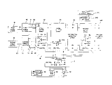
7 Referring to Figure 1, the redundant
8 transmitters are illustrated by the first signal
9 source lû and second signal source 2û which is
lû independent of the first signal source 10. The first
11 signal source 10 provides its signal via line 30 to
12 first power divider 40 which distributes the signal to
13 various outputs 51, 52, 53, 54 of the first power
14 divider 40. Similarly, second signal source 20
provides its signal via line 6û to second power
16 divider 70 which distributes the provided signal to
17 its various outputs 81, 82, 83, 84. The outputs of
18 power dividers 40 and 70 are provided to a first
19 switch array 90.
Switch array 90 is a group of single-pole,
21 double-throw switches 100. Each SPDT switch 100 has
22 inputs 101 and 102 with a single output 103. The
23 position of each switch is controlled by either the
24 main beam steering unit (BSU) 150 or standby BSU 140.
Generally, each input 101 of each SPDT switch 100
26 would be connected to one of the outputs 51, 52, 53,
~31~ 2
1 54 of ~irst power divide:r 40. The correspondinq input
2 102 of SPDT switch 100 would be connected ko one of
3 the corresponding outputs 81, 82, 83, 84 of second
4 power divider 70. In normal operation, the firs-t
signal source would be selected and would provide
6 power to the system via the first power divider 40 and
7 all SPDT switches 100 would be in the UP position so
8 that each input 101 would be connected to switch
9 output 103. Upon detection of a failure in the first
signal source 10, BSU 150 would operate the SPDT
11 switches 100 via control 104 and move each switch 100
12 to the DOWN position so that input 102 would be
13 connected to switch output 103. This would result in
14 the second signal source 20 via power divider 70
providing the necessary rf power to the MLS. As a
16 result, failure of one of the SPDT switches 100 does
17 not totally disable the MLS and would only affect the
18 particular port through which the failed switch is
19 connected.
The outputs of first switch arra~/ 90 are
21 connected to phase shifter array 120 for controlling
22 the scanning of the radiated beam in response to
23 controls provided by either BSU 130 or standby BSU 140
24 via third switch array 131. Switch array 131 is a
group of single polej double throw switches 132. Each
26 SPDT switch 132 has inputs 133, 134 with a single
-10-
~ 3 ~
1 output 135. The position of each switch is controlled
2 by either the main BSU 13û or standby BSU 14û.
3 Generally, each input 133 of each SPDT switch 132
4 would be connected to one of the outputs of main BSU
13û. The corresponding input 134 of SPDT switch 132
6 would be connected to one of the corresponding outputs
7 of standby BSU 14û. In normal operation, the main BSU
8 130 would be selected and would provide control
9 signals to phase shifter array 120. All SPDT switches
132 would be in the LEFT position so that each input
11 133 would be connected to switch output 135. Upon
12 detection of a failure of the main BSU 130, monitor
13 and switchover logic 150 would operate the SPDT
14 switches 132 and move each to the RIGHT position so
that input 134 would be connected to switch output
16 135. This would result in the standby BSU 14û
17 providing control signals to phase shifter array 120.
18 As a result, failure of any one of the SPDT switches
19 132 does not create a single point system failure and
cannot totally disable the MLS. A switch failure
21 woùld only affect the particular phase shifter with
22 which the failed switch is associated.
23 Generally, control of the system operation
24 would be un~er main BSU 13û in coordination with
monitor and switchover logic 150. Logic 150 is
26 constantly analyzing various monitor outputs provided
~ 3 ~
1 by one or more rnonltors (not shown). As shown in
2Figure 1, each BSU 1~0, 140 controls ~he first switch
3 array 9û, the second switch array 170 (described
4 below) and the third switch array 131. The controls
are illustrated in this manner because, as shown in
6 Figure 2, this facilitates a modular configuration.
7 There may also be a requirement for redundancy (not
8 illustrated) with regard to monitors 15û.
9The outputs from phase shifter array 12û
lû which include phase shifted signals are then provided
11 via distributed amplifier array 160 to second switch
12 array 17û. Amplifier array 160 is a plurality of
13 in-line amplifiers, one for each output port of the
14 phase shifter array 120. Switch array 17û is a group
of single pole, double throw switches 180. Each
16 switch has an input 181 and two outputs 182, 183.
17 Each output 182 is connected to a corresponding
18 element of the primary element array 190 to power the
19 primary antenna elements for providing a scanning MLS
2û beam. Each output 183 is connected to the
21 corresponding input of recombining network 2ûO for
22 powering the auxiliary antenna elements. The position
23 of each SPDT switch 180 of second switch array 170 is
24 controlled by BSU 130 or BSU 140 via third switch
array 131. In the DOWN position, each SPDT switch 180
26 powers the primary element array l9û via output 183.
-12~
~ 3 ~ 2
1 In the UP position, each SPDT switch 180 powers the
2 recombining network 200 via output 182.
3 As with the -firs-t switch array 9û, the
4 second switch array permits supplied energy signals to
be either supplied to the primary element array l9û or
6 to the auxiliary element array 21û without the
7 supplying of such signals being dependent upon any one
8 single-pole, double-throw switch or being subject to
9 any single point failure.
lû An MLS generally has several modes o-f
11 operation. In one mode, a Tû-FR0 beam is scanned in
12 order to provide aircraft within the scanning beam
13 azimuth or elevation information. In other modes of
14 operation, auxiliary antennas radiate signals which
provide supplemental landing information. Primary
16 element array 190 includes a plurality of antenna
17 elements which, when supplied by wave energy signals,
18 provide a beam of radiated energy. The beam is
19 electronically scanned Tû and FR0 by varying the phase
2û of the input signals to the antenna elements. The
21 phase is varied by phase shifters 120.
22 During auxiliary operationJ one or more
23 auxiliary antennas radiate information. Auxiliary
24 element array 210 is a grouping of various auxiliary
antennas which are used to provide the supplemental
26 information to aircraft within the range of the MLS.
-13-
~ 3 ~
1 In the prior art, auxiLiary antennas are generally
2 powered directly by the siqnal source. As indicated
3 abûve, an antenna switch is used to select the
4 particular antenna or group of antennas which are
connected to the signal source. As a result, the
6 reliability of the auxiliary antenna operation is
7 dependent upon the single antenna switch which selects
8 the antenna and connects it to the signal source.
9 In contrast, the invention employs a
second switch array 17û which supplies power to a
11 recombining network 2ûû to feed the auxiliary element
12 array 210. During auxiliary operation of the MLS,
13 each SPDT switch 180 is in the DOWN position so that
14 supplied signals are provided to recombining network
2ûû. The number of inputs to recombining network 2ûO
16 equals the number of inputs to primary element array
17 110. The number of outputs for recombining network 200
18 depends upon the number of elements in the auxiliary
19 element array and may be, for example, four or eight.
2û Recombining network 20û is any standard network, such
21 as a Blass or Butler array, which recombines the
22 signals at the input according to a predetermined
23 coupling arrangement and provides the combined signals
24 at the outputs of the network 200.
During auxiliary operation, the beam
26 steering unit 130 controls the phase shifters 120 so
-14-
$ ~ 2
1 -that the phase o~ the signals input into the
2 recombining network 2ûû result in illuminating the
3 partlcular output of network 200 which is connected to
4 the particular auxiliary antenna of array 210. For
example, assume that the OCI auxiliary antenna mus-t be
6 illuminated. Also, assume that the ûCI antenna is
7 connected to the first output port of recombining
8 network 2ûO. Since the characteristics of the
9 recombining network are known and the coupling
lû arrangement within the network preset, appropriate
11 illumination of the inputs of network 20û will result
12 in output 1 being primarily illuminated. In this way,
13 the operation of each auxiliary antenna is not
1~ dependent on any single antenna switch.
Figure 2 illustrates one preferred
16 embodiment of the invention of Figure 1. Dual signal
17 sources 300 and 301 separately feed dual power
18 dividers 302, 3û3. In particular, a first transmitter
19 (TXl) feeds the first power divider 302 and a second
transmitter (TX2) feeds the second power divider 303.
21 The outputs of each of the power dividers is connected
22 to the input to one of the modules 305-308 which
23 includes a single pole, double throw switch 3û5a-308a,
24 a phase shifter 305b-308b, a second single pole,
double throw switch 305c-308c and a third single pole,
26 double throw switch 3û5d-3û8d. Modules 3û5-308
~15-
~ 3~ '2
1 comprise the combination o~ ~irst switch array 90,
2 phase shifters 120, second switch array 170 and third
3 switch array 131 as illustrated in Figure 1. Main ~SU
4 bus 311 provides the control signals between main BSU
309 and each of the SPDT switches. Main BSU bus 311
6 also provides one of the input signals to SPDT
7 305d-3û8d. Standby BSU bus 312 provides switch
8 control signals and the other input signal to SPDT
9 305d-308d. For simplicity, connectors to the switches
lû from the BSUs are illustrated as buses. However, each
11 SPDT may be directly connected to a separate port of
12 the BSU.
13 Single pole, double throw switches
14 305a-308a correspond to the first switch array 90 of
Figure 1. Switches 305c-308c correspond to the second
16 switch array 170. Switches 3û5d-308d correspond to
17 the third switch array 131. Phase shifters 305b-308b
18 correspond to phase shifter array 120. Amplifiers
19 3û5e-308e correspond to the distributed amplifier
array 160. Elements 33û-333 correspond to the primary
21 element array 19û.
22 ûperation of the preferred embodiment
23 illustrated in Figure 2 is as follows. During
24 scanning cycles, main BSU 309 instructs the switches
via bus 311. Switches 305a-308a are placedjin the UP
26 position, switches 305c-308c are placed in the ûOWN
-16-
~ 3 ~ 2
1 position and switches 305d-308d are olaced ir~ the UP
2 position. This results in transmitter 300 providing
3 signals via the first power divider 302 to -the primary
4 antenna elements 33û-333. In addition, phase shifters
305b-308b receive control signals frorn the main BSU
6 309 via bus 311 which result in the scanning of the
7 beam ra~iated by elements 33û-333. During auxiliary
8 modes, main BSU 309 would place switches 305c 308c in
9 the UP position. This would result in supplied wave
energy signals being provided to recombining network
11 350. In addition, main BSU 317 would control phase
12 shifters 305b-308b so that the phased signals being
13 provided to recombining network 350 would illuminate
14 the appropriate auxiliary antenna port. This aspect
of the invention is described in more detail below.
16 In contrast, during scanning modes, main BSU is
17 adjusting the phase shifter 3û5b-308b to radiate a
18 scanning beam via the primary array of elements
1~ 330-333.
In the event of a failure, monitor and
21 switchover logic 320 would evaluate the failure and
22 correct the problem. Logic 320 may be advised of a
23 failure via field monitors, inherent monitors within
24 the system, information derived from built in test
equipment or from information provided by external
26 sources. For example, if prlmary signal source 3ûO
1 were inoperative, main BSU 309 would instruct SPDT
2 switches 305a-308a -to switch to the DOWN position.
3 This instruction would be provided via main bus 311 so
4 that power divider 303 would be supplying the input
signals via secondary source 301. If a failure in the
6 main beam steering unit 317 is detected, standby BSU
7 310 controls switches 305d-308d and places the
8 switches in the DOWN position so that standby BSU 310
9 is providing control signals via bus 312 to phase
shifters 305b-308b.
11 Figure 3 illustrates one embodiment of
12 recombining network 350 in the form of a Butler
13 (factorial) array matrix having 100% circuit
14 efficiency. Recombining network 350 has input ports
1, 2, 3 and 4, linked by phase shifters 351 and
16 couplers Cll, C12, C13, C21 and C22 to
17 output ports A and B. This forms a four element, two
18 beam matrix. Providing signals of phase Ell, E12,
19 E13 and E14 to input ports 1-4, respectively, will
result in illuminating output port A. On the other
21 hand, providing signals of phase E21, E22, E23
22 and E24 to input ports 1-4, respectively, will
23 result in illurnination of the output port B. For a
24 more detalled description of the operation of such
arrays see Microwave Scanning Antennas edited by R. C.
26 Hansen, Chapter 3, Academic Press, 1966.
-18-
1 For example, a data antenna rnay be ~ 3~ ~g 6
2 connected to output port A and an OCI antenna to
3 output port B. During ûCI cycles, main BSU places
4 switches 305c-308c in the UP position and provides
signals to the input ports l-ll having phases E21,
6 E22, E23 and E24, respectively. During data
7 cycles, main BSU 309 places switches 305c-308c in the
8 UP position and provides signals to the input ports
9 1-4 of recombining network 350 at the phases Ell,
E12, E13, E14, respectively. This results in
11 illumination of only port A and transmission of such
12 information by the data antenna. The selection of the
13 data and OCI antennas, therefore, does not depend upon
14 any single rf switch.
Figures 4, 5 and 6 illustrate various
16 alternative embodiments of the invention. The same
17 reference characters have been used for the same
18 structure which appears in Figures 1, 4, 5 and 6.
19 In Figure 4, the recombining network
becomes unnecessary if the data antenna is the only
21 auxiliary antenna which is considered critical to the
22 operation of the system. Antenna switch 400 is
23 located between power source 10 and first power
24 divider 40. A second antenna switch 401 is located
between power source 20 and second power divider 70.
26 During auxiliary modes of operation, the controlling
19-
~ 3 ~ 2
1 beam steering unit activates the apPrOpriate antenna
2 switch to provide a signal for radiation by the
3 selected data antenna. Durinq normal operation in the
4 scanning mode, antenna switch 4ûO would connect pûwer
supply lû to first power divider 40. During normal
6 operation in the auxiliary mode, antenna switch 400
7 would connect power supply 10 to first data antenna
8 411. During the back-up scanning mode, antenna switch
9 401 would connect power supply 20 to second power
lû divider 70. During back-up operation of the auxiliary
11 mode, power supply 20 would be connected to second
12 data antenna 411 via antenna switch 401. In Figure 4,
13 main BSU 130 is shown as having control bus 412
14 connected to phase shifter array 120, first switch
array 90 and antenna switches 400 and 401 to control
16 the operation of these subsystems. Similarly, standby
17 BSU 140 is connected by standby bus 413 to the same
18 subsystems. Alternatively, the main BSU 130 and
19 standby BSU 140 may be connected to the subsystems via
a third switch array as illustrated in Figure 1 or by
21 an array of OR gates or other logic circuits which
22 would function as switches.
23 Figure 5 illustrates another alternative
24 embodiment of the invention in which a passive ferrite
circulator 402 is used to interconnect the alternative
26 power sources to power divider 403. Circulator 402 is
-20-
1 a standard passive ferrumagrlekic device such as a
2 passive waveguide junction. Each port A, B, C of
3 circulator 402 is -related to the other such that when
4 power is fed to any one port, it is transferred to the
next port as indicated by the arrow. The invention as
6 illustrated in Figure 5 would be useful when it is
7 unnecessary to employ switching arrays such as
8 switching array 90, 131 or 170. Although circulator
9 402 and power divider 403 can be considered single
point failures, both these devices are passive and
11 have a very high reliability rate.
12 In the normal scanning mode, antenna
13 switch 400 would connect power supply 10 to circulator
14 port A. Single pole, single throw switch 415 would be
closed so that the circulator would transfer power
16 from port A to port C which is connected to power
17 divider 403. During normal operation of the auxiliary
18 mode, antenna switch 400 would connect power supply 10
19 to first data antenna 410. During back-up operation
in the scanning mode, power supply 20 would be
21 connected to power divider 403 via antenna switch 401
22 and circulator 402. Switch 415 would be open so that
23 the circulator would view port A as an open circuit
24 and would transfer the power supplied to port B to
port C by bypassing port B. In the back-up auxiliary
26 mode, antenna switch 401 would interconnect second
27 data antenna 411 to power supply 20.
-21-
~ 3 ~ 2
1 A short circuit failure of` switch 415 does
2 not cause a signal critical failure because it
3 continues -to connect primary power source 10 to power
4 divider 403 via circulator 402. An open circuit
f`ailure of switch 415 would automatically cause
6 switchover to the back up supply 20 which in fact
7 requires an open circuit switch 415 to transfer the
8 amplified carrier to the array power divider 4û3.
9 Therefore, the combination of circulator 402 and
switch 415 provide a fail-operational configuration.
11 Figure 6 illustrates another alternative
12 embodiment of the invention wherein circulator 402 is
13 used in the same manner as Figure 5 to alternatively
14 connect the signal sources to power divider 403. In
addition, second switching array 170 and third switch
16 array 131 are used as described above.
17 While there have been described what are
18 at present considered to be the preferred embodiments
19 of this invention, it will be obvious to those skilled
in the art that various changes and modifications may
21 be made therein without departing from the invention
22 and it is, therefore, aimed to cover all such changes
23 and modifications as fall within the true spirit and
24 scope of the invention.
-22-