Note : Les descriptions sont présentées dans la langue officielle dans laquelle elles ont été soumises.
132420~
SYSTEM FOR DETECTING SURROUNDING ENVIRONMENTAL
CONDITIONS USING A MULTIPLE NUMBER OF INCOMING SIGNALS
BACKGROUND OF THE INVENTION
.
The present invention relates to a detection system for
receiving incoming signals coming from many di~ferent directions
and presenting indications of the direction and/or range of a
source of incoming signals. More particularly, it relates to a
detection system which comprises ~i) means for receiving incoming
signals in a manner that the Doppler effect is produced to vary
J,.'
the carrier frequency of the incoming signals, ~ii) a matched
filter coupled to the receiving means to pulse-compress output
,~ 10 signals therefrom, and (iii) an indicator for displaying output
signals from the matched filter, and which forms a plurality of
reception beams successively in angular directions. This type
of detection system is disclosed in U.S. Patent No. 4,425,634.
Prior art detection systems will be described hereinbelow
in conjunction with the drawings.
;
SUMMARY OF THE INVENTION
Accordingly, an object of the present invention is to
provide a detection system which is greatly reduced in size
without degrading the performance of the system, so that it is
easy to handle and to be maintained.
B
,
. -
,
` 132~2~3
Another ob~ect of the invention is to provide a detection
system which is capable of successively deriving output signals
of each of the ultrasonic transducers with lesser number of
preamplifiers, thereby reducing the dimensions of the receiving
unit, manufacturing cost thereof and the electric power
-
consumption thereof.
Another ob;ect of the invention is to provide a detection
:~ system which derives the reception signals produced by the
~ ultrasonic transducers by means of a switch incorporated between
; 10 the transducers and the input terminals of the preamplifiers and
another switch incorporated between the output terminals of the
preamplifiers and the input terminal of a beamformer.
In accordance with one aspect of the invention there is
provided a detection system for receiving incoming signals from
~` 15 a plurality of directions in a manner such that a Doppler effect
~ is produced to vary a carrier frequency of the incoming signals
`. and for presenting a display resulting from the received incoming
} signals on an indicator, comprising: a plurality of ultrasonic
transducers for receiving incoming signals; a plurality of
preamplifiers for amplifying reception signals produced by said
ultrasonic transducers; first coupling means for connecting at
least two ultrasonic transducers to a single preamplifier; a
filter for pulse-compressing said reception signals produced by
` 132~2~
sa d ultrasonic transducers; second coupling means for
successively coupling output terminals of said preamplifiers to
an input terminal of said filter; and an indicator for displaying
; output signals from said filter.
t:
` 5 BRI~F D~SCRIPTION OF THE DRAWINGS
In the drawings:
Fig. 1 shows a schematic block diagram of a relevant
principle portion of an embodiment according to the present
~` invention,
'~:
10Fig. 2 shows a time sequence diagram illustrating how the
~- switches in Fig. 1 are operated, and how the ultrasonic
transducers and th~ input terminal of the beamformer are coupled,
Fig. 3 shows a circuit configuration of a portion of a
switch SWa of an embodiment according to the invention shown in
15Fig. 6,
s Fig. 4 shows a circuit configuration of a signal generator
producing control signals for controlling field effect
transistors as shown in Fig. 3,
Fig. 5 shows a time sequence diagram illustrating how
20switches SWa, SWbl and SWb2 shown in Fig. 6 are operated, i.e.,
how the input terminal of the beamformer is coupled to
transducers,
Fig. 6 shows a block diagram of an embodiment according to
the invention,
132420~
.. .
Fig. 7 shows amplitude variations of input signals applied
at the two input terminals of the multipliers 11 and 12 shown in
Fig. 6,
~" Figs. 8, 9 and 10 show response characteristics of a filter
., .
included in each of the preamplifiers shown in Figs. 1, 3 and 6,
Fig. 11 shows a block diagram of each of the preampli~iers
used in an embodiment of the invention,
^s`~ Fig. 12 shows a schematic block diagram of a relevant part
of a prior art detection system, and
Fig. 13 shows another circuit configuration of the signal
~.~
`; generator producing control signals for controlling field-effect
transistors as shown in Fig. 3.
Throughout the drawings, the same reference numerals and
symbols are given to like components.
lS Hereinafter, the invention will be described as embodied in
~ .
a scanning sonar for receiving incoming signals from many
different directions in a wide range of angles to indicate the
direction and range of objects on the face of an indicator.
Referring to Fig. 12 in which a relevant portion of a prior
art detection system is shown, one hundred and twenty ultrasonic
¦ transducers lCH through 120CH are disposed on an imaginary circle
¦ as equidistantly spaced, which forms one row of transducers.
Preamplifiers P1 through P120 amplify reception signals caught
by the ultrasonic transducers lCH through 12OCH respectively.
ZS A sel-ctor S- succ-sniv-ly conn cts, at a pred-termlned speed,
,~
,~
i
13242~
the output terminal of each of the preamplifiers Pl through P120
to the inpUt terminal of a beamformer BM to supply the beamformer
with the output signals of each of the preamplifiers Pl through
Pl20. As a result, the Doppler effect is produced to vary the
carrier freguency of the incoming signals received. The
;~ beamformer comprising a matched filter pulse-compresses the
received signals to produce signals having come in a desired
direction and detected. The reception signals produced by each
of the transducers lCH through 120CH are selected and derived at
the output terminals of the preamplifiers P1 through P120 to be
supplied to the input terminal of the beamformer.
With the prior art detection system, six rows of ultrasonic
transducers are disposed in parallel with each other on the
surface of a cylinder along the circumference thereof, with each
row comprising one hundred and twenty ultrasonic transducers.
Thus, seven hundred and twenty ultrasonic transducers are
disposed on the surface of a cylinder, and the same number of
preamplifiers are required to be incorporated in the receiving
unit of the detection system, since all the ultrasonic
transducers are separately and respectively connected to the
corresponding preamplifiers. The switch SW is incorporated
between the output terminals of the preamplifiers P1 through P120
and the input terminal of the beamfor~er, and the reception
signals produced by each of the transducers lCH through 120CH are
selected by the switch SW to be applied at the input terminal of
- , l32~2a~
tho beamformer BM. Accordingly, the dimensions of the receiving
unit and the electric power consumed by the receiving unit are
determined by the number of the preamplifiers. Manufacturing
cost of the receiving unit is substantially determined by the
- 5 cost of the preamplifiers.
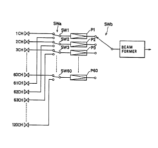
Referring to Fig. 1 and Fig. 2, the principle of the present
invention will be explained hereinafter. one hundred and twenty
reception transducers lCH through 120CH are disposed on a circle
;~ as equidistantly spaced. These transducers are divided into two
groups, with one group including the transducers lC~ through
; 60CH, and with the other group having the transducers 61CH
through 120CH. The input texminal of each of preamplifiers P1
through P60 is alternately connected by means of a switch SWa to
corresponding one transducer of the two transducer groups, i.e.,
the transducers lCH through 60CH and the transducers 61CH through
~` 120CH. The switch SWa comprises sixty switch elements SW1
through SW60. A switch SWb successively connects the output
terminals of the preamplifiers P1 through P60 to the input
terminal of a beamformer BM. The switch SWb is comprised of
digitally controlled analog switches, for example, of analog
multiplexers the MC14051Bs manufactured by Motorola Inc. Thus,
the reception signals amplified by the preamplifiers Pl through
P60 are successively derived and supplied to the beamformer BM.
.~
i32~2G~
Referring to Fig. 2, the portions designated as (a) through
(e) illUstrate how the switeh SWa eomprising sixty switch
elements SWl through sw60 is operated. Symbols lCH through 120CH
in brackets are the ones assigned to the ultrasonic transducers.
Thus, there is illustrated the way how the ultrasonic transducers
are conneeted to the input terminals of corresponding
preamplifiers. The portions designated as (f) through (j)
illustrate how the switeh SWb is operated, i.e., how the output
terminal o~ a preamplifier corresponding to transdueer is
" 10 eonnected to the input terminal of the beamformer. Symbols lCH
-through 120CH are also the ones assigned to the transducers. It
will be apparent from the time sequenee diagrams that the
ultrasonic transducers lCH through 120CH are suceessively coupled
to the input terminal of the beamformer BM by means of the
;~ 15 switches SWa and SWb whieh are controlled by a controller.
~- Referring to Fig. 6, one hundred and twenty ultrasonie
i'
.electrostrictive transducers lCH through 120CH are disposed on
a circle as equidistantly spaeed. These transducers are divided
into two groups, with the one group ineluding the transducers lCH
through 60CH and the other group eonsisting of the transducers
61CH through 120CH. The input ter~inal of each of the
preamplifiers Pl through P60 is connected by means of a switch
SWa to corresponding one of the transducers of each of the two
.groups lCH through 60CH and 61CH through 120CH. The switch SWa
comprises sixty switching elements SWl through SW60.
. ~ .
132~2~
The switching element SW1 alternately connects the input
terminal of ~he preamplifier P1 to one of the transducers
lCH and 61CH. The switching element SW2 connects the input
terminal of the preamplifier P2 to one of the transducers
2CH and 62CH. In the same way, each of the switching
elements SW3 through SW60 alternately connects the input
terminal of one of the preamplifiers P3 through P60 to one
transducer of each corresponding pair of the transducers
3CH and 63CH through 60CH and 120CH. A s~itch SWbl
comprises thirty switching elements which successively
connect the output terminals of the odd-numbered
preamplifiers P1, P3, , P59 to the input terminal of
a multiplier 11. A switch SWb2 comprises thirty switching
elements which successively connect the output terminals
of the even-numbered preamplifiers P2, P4, , P60 to
the input tenminal of a multiplier 12. A switch select
control circuit 10 controls the switches SWa, SWbl and
SWb2 to select switching elements to perform connecting
and disconnecting operations as desired. me switch SWa
firstly and successively connects the input terminal of
each of the preamplifiers P1 through P60 to corresponding
one of the ultrasonic transducers 1CH through 60CH, and
then successively connects the input terminal of each of
the preamplifiers P1 through P60 in the order of P1, P2,
. . , P60 to corresponding one of the transducers 61CH
through 120CH. me switches SWbl and SWb2 successively and
respectively connect the output terminals of the odd-
-` 132~2~
numbered and even-numbered preamplifiers P1 through P60 to
the input terminals of the multipliers 11 and 12 so that
the output terminals of the preamplifiers P1 through P60
are successi~ely coupled to the input terminal of the
beamformer. A signal generator 13 produces triangular
waveform signals which are shifted in phase from each
other, and supplies the multipliers 11 and 12 with these
shaped signals designated as ~c~ and ~d~ (shown in Fig. 7)
at the other inputs thereof respectively. The multiplier
11 multiplies the reception signals designated as ~a~
(shown in Fig. 7) supplied from the preamplifiers at the
one input thereof by triangular wave signals desiqnated as
c~ (shown in Fig. 7) supplied at the other input terminal
thereof, and supplies an adder 14 with the resultant
signals at one input terminal thereof. The multiplier 12
~i multiplies the reception signals designated as ~b~ (shown
in Fig. 7) supplied from the preamplifiers at the one
input terminal thereof by triangular wave signals
designated as ~d~ (shown in Fig. 7) supplied at the other
input thereof, and supplies the adder 14 with the
' resultant signals at the other input thereof. The adder 14
adds the signals supplied to the two input terminals to
one another, and supplies the resultant added signals to a
signal input terminal of an analog-delay circuit 15.
The relationship between the signals desiqnated as
~a~, ~b~, ~c~ and ~d~ is as shown in Fig. 7. In Fig. 7a
and Fig. 7b, the numerals qiven to each block correspond
_ g_
'
- , l32~2a~
to the numbers assigned to th~ ultrasonic transdu~ers 1CH
through 120CH. As will be apparent, the reception signals
produced by two adjacent transducers are increasingly or
decreasingly weighted with time to average the reception
}
s signals, thereby obtaining the same signals as received by
one ultrasonic transducer mechanically rotated at a
~, constant speed.
The analog-delay circuit 15 has a plurality of
i.e., n output terminals as equidistantly spaced, and
stores the reception signals produced by ultrasonic
' transducers of a group used for forming a reception beam.
Resistors rl, r2, r3, rn are inserted between the
corresponding output terminals of the analog-delay circuit
15 and one input terminal of operational amplifiers 16 and
` 17. To the one input of the operational amplifier 16,
r signals obtained by sampling the positive portions of the
input signals applied at the input of the analog-delay
circuit 15 are supplied. To the one input of the
operational amplifier 17, signals obtained by sampling the
negative portions of the signals inputted to the delay
circuit 15 are supplied. me output terminal of the
operational amplifiers 16 and 17 are connected to the two
input terminals of an operational amplifier 18
respectively. me input signals applied at the signal
input of the delay circuit 15 are ad~anced therein each
time a clock pusle is applied at the clock input of the
circuit 15, and the signals stored therein appear at the
--10-- .
.
corresponding output terminals. m ~se output signals of
the analog-delay circuit 15 are weighted by the resistors
rl, r2, r3, , rn and resistors R1 and R2 inserted
between the one input terminals of the operational
amplifiers 16 and 17 and the output terminals thereof
respectively to produce resultant signals which are added
to one another by the operational amplifier 18. The values
of the resistors rl, r2, r3, , rn and resistors R1
and R2 are respectively determined in such a way that the
amplitude of the signals from a sound source in a desired
direction becomes maximum with respect to that of other
incoming signals from the other directions when a first
signal supplied at the signal input of the analog-delay
circuit reaches the right end thereof and all the output
signals appear at the respecti~e output terminals thereof.
Thus, a matched filter is formed by the analog-delay
circuit 15, resistors rl, r2, r3, , rn, operational
amplifiers 16, 17 and 18, and resistors Rl, R2, R3 and R4.
An amplifier 21 amplifies the output signals from
the operational amplifier 18 containing only the incoming
signals having come from a desired direction, and supplies
the resultant amplified signals to the input terminal of
an indicator 22 comprising, for example, a cathode-ray
tube. A deflection circuit 23 produces deflection signals
for deflecting the electron beams of the cathode-ray tube
concentrically. A controller 20 produces timing control
signals, and supplies the switch select control circuit
.
13242`~g
10, signal generator 13, analog-delay circuit 15 and
deflection circuit 23 with the respective control signals.
Referring to Fig. 3, one output terminal of the
~; ultrasonic transducer lCH is connected to the source
ri terminal of a depletion-mode p-channel junction field-
effect transistor (hereinafter called as ~FET~) Q1 such as
" .
2SJ103 manufactured by Toshiba. The drain terminal of the
~' FET Q1 is connected to the input terminal of the
~' preamplifier Pl. One output terminal of the ultrasonic
`~ transducer 61CH is connected to the source terminal of a
':~
FET Q61. The drain terminal of the FET Q61 is also
connected to the input terminal of the preamplifier P1.
e gate terminals of the FETs Q1 and Q61 are respectively
supplied with control signals having a m amplitude level
from the switch select control circuit 10 to switch the
FETs on and to pass therethrough reception signals caught
by the transducers 1CH and 61CH. Two pairs of diodes shown
in Fig. 3 form limiting circuits to limit the amplitude
levels of the input signals supplied to the FETs Q1 and
Q61.
; Fig. 4 shows a circuit diagram for producing the
control signals supplied to the gate terminals of the FETs
such as Ql and Q61 shown in Fig. 3. Referring to Fig. 4,
shift-registers 30 and 31 are connected in series with
each other to have thirty output terminals. To one input
terminal of the shift-register 30, there are supplied FS
signals determining on-off periods of the FETs such as the
-12-
_ !
- ` 132~2~
FETs Q1 and Q61 shown in Fig. 3, while clock pulses are
supplied to the clock input terminal thereof. At
respective output terminals of the shift-registers 30 and
31, there are produced FS signals which are successively
shifted by a time equivalent to the recurrence period of
the clock pulses. A waveform conversion circuit 32 is
comprised of an operational amplifier, a condenser, a
resistor and zener diodes, and functions to convert an FS
signal shaped in a rectangular form into a substantial
trapezoid waveform. A signal level lowering circuit 33 is
comprised of an operational amplifier and resistors. A
signal level conversion circuit 36 functions to raise the
voltage level of the output signals of the signal level
lowering circuit 33 to the"pinch-off voltage of the FET. A
polar'ity inversion circuit 34 is comprised of an
operational amplifier and resistors, and functions to
inverse the polarity of the output signals of the signal
level lowering circuit 33. A signal level conversion
circuit 35 is constructed in the same way as the signal
level conversion circuit 36. The output signal of the
signal level conversion circuit 35 is supplied to the gate
terminals of the FETs Q1 and Q2. The output signal of the
signal level conversion circuit 36 is supplied to the gate
terminals of the FETs Q61 and Q62. In the same way, the
output terminals of the other signal level conversion
circuits are respectively coupled to the gate terminals of
a corresponding pair of the FETs . m us, the switching
-13-
` ` 132~2û,~
~ . .
elements i.e., the FETs are driven b~ rectangular waveform
signals, the leading and trailing edges of which are
rounded off at the upper and lower points thereof. The use
of such modified signals suppresses high frequency
components included in the control signals, thereby
drastically reducing noises produced when switching
operations are performed by the FETs.
Referring to Fig. 5, the portions desiganted as
(1) through (10) illustrate how the switch SWa is
operated. Numerals in brackets correspond to the numbers
assigned to the ultrasonic transducers 1CH through 120CH.
The portions designated as (11) through (20) illustrate
how the switches SWb1 and SWb2 are switched on and off.
Numerals in this part of the figure respectively
correspond to the transducers supplying their output
signals to the corresponding preamplifiers. In this
embodiment of the invention, as shown in Fig. 5 (1)
through (10), pairs of two adjacent transducers such as
lCH and 2CH, 3CH and 4CH are connected to or disconnected
from corresponding preamplifiers P1 through P4 at the same
time. This arranqement reduces the number of the drive
circuits shown in Fig. 4 for the switching elements by
one-half.
Some aspects of the filter included in the
preamplifier will be explained hereinafter. In the
foregoing embodiment of the invention, for example, to the
input of the preamplifier P1, the reception signals caught
-14-
:` 132~2~53
by the transducers 1CH and 61CH are alternately supplied.
When the FETs Q1 and Q61 are respectively switched on and
off for connecting the transducers 1CH and 61CH to the
input terminal of the preamplifier P1 and disconnecting
the transducers therefrom, noises are produced and are
also applied at the input terminal of the preamplifier.
The noises are prominent in terms of amplitude with
respect to the reception signals applied at the input
terminal of the preamplifier, since the reception signals
transmitted from the transducers thereto are weak and
small ones. Further, the reception signals in rectangular
shapes applied at the input terminal of the preamplifiers
are rounded off thereby at the leading and trailing edges
of the signals, since the frequency characteristics of the
preamplifiers are of narrow bandwidth. The phenomena are
illustrated in Fig. 8. Referring to Fig. 8, "Ta~ shows an
instant at which the reception signals produced by the
transducer 1CH are sampled, while ~Tb~ shows an instant at
which the reception signals produced by the transducer
61CH are sampled. If a noise tail resulting from the
switching operation in relation to the transducer 61CH is
still existing at the instant ~Ta~, the noise tail becomes
noises having directional information, thereby decreasing
the S/N ratio. While, if a noise tail resulting from the
switching operation in relation to the transducer lCH is
still existin~ at the instant ~Tb~, the noise will be
crosstalk to the signals produced by the transducer 61CH.
-15-
` ~`` 132~!2~
Accordingly, effects caused by the noise tail have to be
reduced in designing the filter included in the
preamplifier.
Referring to Fig. 11, a mixer 40 is supplied with
:
the reception signals with their frequency ~fi~ from the
corresponding transducers at one input terminal thereof,
and with signals ha~ing their frequency "fl~ from a local
oscillator at the other input terminal thereof, and
performes frequency conversion to produce output signals
with their frequency ~fo = fi - fl~ to the input terminal
of an amplifier 41 for amplifying the input signals. A
bandpass filter 42 passes the signals having frequencies
within a predetermined frequency range. The effects
explained above are reduced by appropriately designing the
frequency characteristics of the filter 42.
With regard to noises produced by a
corresponding FET when switched on and off, impulse
response is first analyzed which is possessed by the
filter. Fig. 9 shows a waveform illustrating an impulse
response for the filter. The time ~ts~ represents a period
from a time instant at which a switching noise is produced
to another time instant at which signals are sampled. The
filter is designed to have an impulse response, the value
of which becomes smaller than a predetermined value with
respect to the amplitude of the reception signals at the
time instant when the signals are sampled.
With regard to a signal tail resulting from the
-16-
.
,
` `` ` 1324l2~
reception signals, the filter response to a burst signal
is analyzed. Fig. 10 shows burst signals and resultant
~.
response waveforms. Here, ~to" represents delay time, and
~`- is given by phase spectrum inclination in the frequency
~` range of the filter. ~tr~ is rise time, and is inversely
~;;
proportional to the frequency bandwidth of the filter.
Further, the amplitude of ripples included in a tail
portion is obtained by analysing the variation of a
`~ sinusoidal integral function. In this way, the filter
, characteristics are determined in such a way that the
impulse response of the filter against burst signals is
analyzed, and th difference between the amplitude of the
reception signals produced by the transducer 1CH and that
of the reception signals produced by the transducer 61CH,
i.e., crosstalk ratio becomes greater than a predetermined
level.
` Reduction of the switching noises and improvement
of decoupling the crosstalk are attained by widening the
freguency bandwidth of the preamplifiers. But, improper
i widening of the bandwidth results in decreasing the S/N
ratio. mus, the frequency bandwidth of the filter is
required to be made as narrow as possible. A desired
frequency bandwidth of the preamplifiers is determined
based on the frequency bandwidth in relation to the
Doppler-shift with the carrier freguency and the freguency
bandwidth in relation to the pulse-width of the search
pulse signal radiated into the water. With regard to the
-17-
_ _ .. ... . . _ _ .
132~2~'~
Doppler-shift, the following approximate eguation to
` obtain the frequency bandwidth is used:
+ ~ f1 = 0.7 m f [ Hz ]
`` Herein, m : Ship's relati~e speed with respect
~` to objects detected [ Xnot ]
f : center frequency [ KHz ~
With regard to the pulse-width of the search pulse signal,
the following approximate equation to obtain the frequency
i- bandwidth is used:
x + ~ f2 = 1.3~2~ T
Herein, ~T : pulse-width of the search pulse
signal
;~ It should be noted that although the signal
generator producing control signals for controlling the
FETs is used in the foregoing embodiment, another signal
generator shown in Fig. 13 is also used. Referring to Fig.
13, the signal generator comprises a counter 130, a memory
131, a selector 132, thirty digital-to-analog converters
~ereinafter referred to as ~D-A converters~) 133, 140.
me D-A converter 133 comprises a latch circuit 134
comprising D-type flip-flops, resistors, two operational
amplifiers 135 and 136, two resistors and two condensors.
The operational amplifier 135 produces control signals
supplied to the gate terminals of the FETs Q1 and Q2,
while the operational amplifier 136 produces control
signals supplied to the gate terminals of the FETs Q61 and
Q62. The control signals are formed with the upper and
-l8-
```` ~32~
.
lower flat level portions and curved portions between the
upper and lower levels, with the cur~ed portions being
shaped in sine waveforms. Four output signals appearing at
four output terminals of a group of the latch circuit 134
are respectively welghted with the four respective
resistors, the values of which are respectively
represented as R, R/2, R/4 and R/8. m e resultant weighted
signals are supplied to one input terminal of the
operational amplifier 135. Four output signals appearing
at four output terminals of the other group of the latch
circuit 134 are respecti~ely weighted with the four
resistors. m e resultant weighted signals are supplied to
one input terminal of the operational amplifier 13B. Clock
pulses are supplied to one input terminals of the counter
130 and the selector 132. The counter 130 successively
produces varying count values supplied to the fifteen
input terminals of the memory 131 which comprises a read-
only-memory. The memory 131 stores thirty kinds of digital
signals each representative of two portions of a sine
waveform corresponding to the curved portions of the
signals produced by the D-A converter. The memory 131
supplies digital signals of a group representative of
portions of sine waveforms to the four input terminals of
the latch circuit 134, and also supplies digital signals
of the other group to the selector 132 comprising a
decoder. The selector 132 successively selects the thirty
D-A converters and supplies the latch circuits of the D-A
--lg--
132~2Q~
converters with pulses at the clock input terminals
thereof. The latch circuit 134 produces output signals in
response to the pulses applied at the clock input
terminals thereof.
It should be noted that although the signal
generator 13 produces triangular waves for the multipliers
11 and 12 in the foreqoing embodiment, it can also produce
and transmit sine or cosine waves thereto to obtain the
same result as in the above embodiment.
It should be noted that although only a row of one
hundred and twenty ultrasonic transducers disposed on an
imaginary circle is used in the foregoing embodiment
according to the present invention, a plurality of the
rows of transducers can be arranged vertically as
equidistantly spaced between adjacent two rows of
transducers. miS arrangement enables one to direct the
reception beams in any desired tilt direction by
controlling the phase of the reception signals caught by
transducers disposed on an imaginary vertical line with
respect to one another.
It should be noted that although the number of the
preamplifiers is reduced by one-half in the foregoing
embodiment according to the invention, the number of the
preamplifiers can be reduced by two-thirds by dividing the
ultrasonic transducers into three groups.
While, the invention has been described in detail
nd with reference to specific embodiments thereof, it
-20-
.
132~2~(~
will be apparent to one skilled in the art that variouschanges and modifications can be made therein without
departing from the spirit and scope of invention.
:'
, .
.
~ .
.
Z ~ .
-21-
. .
~' '' ' " . . .