Note : Les descriptions sont présentées dans la langue officielle dans laquelle elles ont été soumises.
~`~
1 326266
--1--
.
PULSE OXIMETER PLETHYSMOGRAPH SYSTEM
This invention relates to osimeters which measure
levels of blood osygenation and, in particular, to a
plethysmograph system for pulse oximetry.
A pulse o~imeter measures the osygen level of blood by
transmitting two different wavelengths of light through a
portion of a subject's body where arterial blood is
flowing. Conveniently this may be a finger or earlobe.
The light which has been transmitted through the body is
detected by a photodetector, which produces a current that
is a function of the pulsatile blood flow. The current
produced in response to each wavelength of light is
measured, and these measurements may be combined by
well-known algorithms such as Bier's Law to produce a
quantification of the osygen content of the blood.
Since the sensor used in the measurement is an
electro-optic device, it can respond to interfering
signals from the other electrical and optical energy
sources. The sensor must respond to changes in light
transmissivity through the body. These physiological
effects contain frequency components in the DC to 50 Hz
band. However, it is desirable that the sensor not
respond to ambient light. Accordingly, the plethysmograph
system should reject ambient light while detecting
physiological signals i~ the bandwidth of interest.
A second category of sources of interference is other
electrical apparatus. Other electrical devices in
hospitals, such as electro-surgical instruments, can
generate radio freguency signals that a plethysmograph
system can pic~ up. It is desirable then to minimize the
sensitivity of the system to interfering signals from
:-96 - ~ ~ ~
-2- 1 326266
sources of this nature.
A known technique for eliminating the interfering
signals descri~ed above is to drive the light sources by a
signal having a frequsncy which is not present in
artificial light or characteristic of other medical
instrumentation. Received signals are then passed through
a bandpass filter to reject siqnals outside the band of
interest, and the filtered signals are then detected by an
en~elope detector. While effective for rejecting unwanted
signals, the energization of the light sources in
alteration hy the driving signal mandates that the
detector be synchronized with the driving signal for ;
correct demodulation. As the following discussion will
show, this arrangement requires undesired widening of the
receiver bandwidth, or electrical connections which
complicate electrical isolation of the light sources and
optical sensor.
In accordance with the principles of the present
invention, the response of a plethysmograph system to
interfering signals is reduced through modulation of the
sensor light sources. The light sources are each
modulated with a characteristic that distinguishes
received signals from each other and that can be
distinguished from ambient light contributions to the
detected signal. The deodulation is performed over
selective bandwidths which further immunizes the system
against radio frequency interference.
In the drawings:
FIGURES 1-3 illustrate spectra resulting from use of
the wa~eform of FIGURES la, lb, 2a, 3a and 6 in freguency
multiplesing in accordance with the principles of the
96 - --
:,
~3~ 1 326266
present invention;
FIGUaE 4 illustrates a bandpass filter response ~or
the waveforms of FIGURES 2 and 3;
FIGURE 5 illustrates a back-to-back configuration of
~EDs;
FIGURE 7 illustrates a preferred embodiment of the
preæent invention; and
FIGURE 8 illustrates waveforms used to esplain the
arrangement of FIGURES 7a-7b.
In a conventional pulse osimeter sensor a light
emitting diode (LED) is used as the light source which
transmits light through tissue. Use of an LED is
desirable due to its dependa~ility, low voltage
reguirement, and narrow optical bandwidth of light
emission. In accordanc~ with the principles of the
present invention, the LED is switched on and off at a
frequency which is subætantially higher than the frequency
range of ambient light (DC) and the physiological signals
of interest ~DC to 50Hz). A photodetector receives the
transmitted light which further contains a component
representative of pulæatile blood flow, the physiological
sign~l, and also receives any ambient light present. The
photodetector signal is passed by a bandpass filter which
is tuned to a significant component freguency of the
switched escitation signal and eshibits a bandwidth
similar to that of the physiological signal. The narrow
bandwidth enables the system to reject interfering signals
at frequencies outside the filter passband, included the
substantially constant (DC~ component resulting from
detection of ambient light. The filter output i5 a
-96
_4_ 1 326266
sinusoidal wave, amplitude modulated with the
~ physiological signal. An amplitude demodulator is
employed to recover the physiological signal.
The freguency multiplesing technique is a significant
improvement over the commonly employed technique of time
division multiplesing. In time division multiplesing the
LED is similarly switched on and off, and the
photodetector signal received when the LED is off, which
0 i8 caused by ambient light, is subtracted from the signal
received when the LED is on. However, due to the need to
preserve the phase relationship between the on and off
states, the receiver bandwidth must estend from DC to
above the escitation signal frequency. Thus, the receiver
employing time division multiplesing is responsive to
wideband noise over this full bandwidth.
.
Referring now to FIGWRE 1, the spectrum of a square
wave Fl of FIGURE la is shown. The spectrum is seen to
fl 20 consist of only odd harmonics of sguare wave Fl, i.e., Fl
3Fl, 5Fl, etc. If the square wave Fl is modulated with a
square wave F0, shown in FIGURE lb, the result is the
f, modulated waveform FO s Fl shown in FIGURE 2a. This
modulated waveform ha8 a spectrum shown in FIGURE 2. The
spectrum of FIGURE 2 consists of the same odd harmonics of
the Fl sguare wave, each with upper and lower sidebands
spaced at odd harmonics of F0 from Fl, i.~. Fl-F0, Fl+F0,
etc. Neither the harmonics of Fl nor the modulation
sidebands occur at frequencies which are even harmonics of
Fl.
In pulse osimetry it is necessary to use LEDs of two
wa~elengths in order to gather signal components which can
be used to compute blood osygenation. Conventionally, one
LED transmits light at a red wavelength, and the other LED
~-96
, , .
.
, .
~r~
~5~ 1 326266
transmits light at an infrared (IR) wavelength. It is
convenient to connect the two LEDs in an o~imeter sensor
in a back-to-back configuration as shown in FIGURE 5,
allowing either LED to be selectively energized by
reversing the applied current and requiring only two
connecting conductors. If a differential voltage drive is
used, capacitive coupling of the LED drive signals to the
detector circuitry, the cable of which is generally in
close prosimity to the LED conductors, can be minimized.
In accordance with the principles of the present
invention, one LED will be driven by a signal with the
spectrum shown in FIGURE 2. The second L~D in the sensor
is switched by a sguare wave F2 of a second frequency,
which is modulated by the F0 sguare wave of FIGURE lb.
The result of this modulation is the F0 s F2 waveform
shown in FIGURE 3a. This waveform has a spectrum as shown
in FIGURE 3. The spectrum shows the odd harmonics of F2
and and 3F2, each with upper and lower sidebands spaced at-
odd harmonics of F0 from F2.
Since the spectrum of FIGURE 2 has no components at F2
and the spectrum of FIGURE 3 has no components at Fl, two
bandpass filters can be used to separate the Fl and F2
signal components from the received signal. FIGURE 4
shows the responses of two filters that may be used to
separate the two desired signals. A bandpass filter -
centered at Fl will respond to the transmission of light
from the LED modulated by the F0 s Fl waveform, and a
bandpass filter centered at F2 will respond to the
transmission of light from the LED modulated by the F0 x
F2 waveform. Each filter must have a bandwidth of at
least twice the bandwidth of the pfflsiological signal,
that is, two times 50Hz - lOOHz, since this information is
contained in sidebands of the center frequency. The
filter must be narrow enough to esclude the nearest
CRK-96
-6- 1 32 62 ~6
- modulation sidebands of the FO square wave, which are F0
above and below the respective center frequencies of the
filters. This is representatively shown in FIGURE 4a,
which is an espansion of a portion of the spectrum of
FIGURE 2. This spectrum shows the center frequency Fl of
the bandpass filter and the filter bandwidth in the range
indicated by the bracket. The Fl-F0 and FllF0 sidebands
are outside the filter pass~and, and the physiological
information signals, indicated as PI, are sidebands of the
center frequency and contained within the passband.
The e~citation signal waveforms o~ FIGURES 2a and 3a
are not suitable for use by back-to-back configured LEDs,
shown in FIGURE 5. This is because the times that the
LEDs are on are time coincident, a physical impossibility
when the LEDs are so connected. FIGURE 6 shows waveforms
that eshibit the spectral characteristics of FIGURES 2 and ,
3 while illuminating only one LED at a time. The sguare
waves Fl, F2, and F0 of FIGURES 6a-6c are combined to
produce the escitation waveforms of FIGURES 6d and 6e.
Specifically, the F0 sguare wave is used to modulate the
Fl square wave such that an escitation pulse is produced
each time F0 and Fl are coincidentally high. This
produces the escitation waveform F0 s Fl shown in FIGURE
6d. The i~verse of the F0 square wave, F0, is used to
modulate the F2 sguare wave to produce the escitation
waveform FO s F2 shown in FIGURE 6e. Thus, the modulating
FO waveform interleaves .the Fl and F2 escitation signals
such that there is no time when the two L~Ds must be
simultaneously turned on.
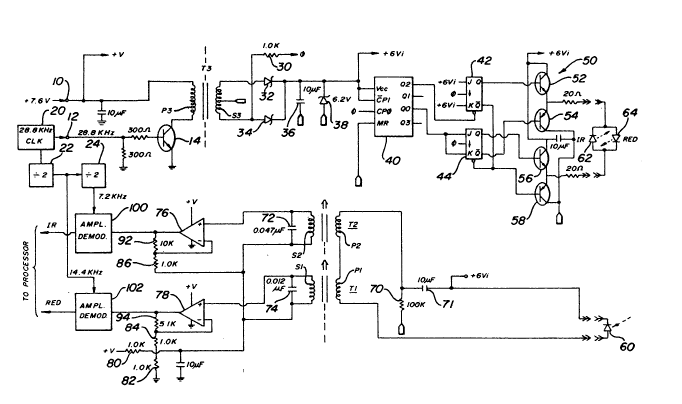
Referring to FIGURE 7, the modulation and demodulation
section and sensor of a pulse o~imeter constructed in
accordance with the principles of the present invention
are shown. In order to minimize electrical hazards to the
CRK-96
-'- 1 326266
patient, the sensor electronics are electrically isolated
from the electronics of the processor by three
transformers Tl, T2 and T3. To energize the sensor
electronics a 28.8kHz clock signal is supplied by a source
20 of clock signals to a terminal 12. The 28.8kHz clock
signal switches a transistor 14, which drives the primary
I winding P3 of transformer T3 . A 7 . 6 volt reference
potential is connected to the other end of the primary
winding P3 to provide a DC voltage ~V for transistor 14
and amplifiers 76, 78, and associated circuits.
The 28.8kHz signal is transformer coupled to the
secondary winding S3 of the transformer T3, which is
center-tapped to the isolated ground of the sensor
electronics. A resistor 30 is coupled to one end of the
secondary winding S3 and provides a 28.8kHz clock
reference signal ~ for the sensor electronics.
~ectifying diodes 32 and 34 are coupled to opposite ends
of the winding S3 to produce a DC supply voltage ~6Vi or
the sensor electronics. The rectified supply voltage ~6Vi
is filtered by a capacitor 36 and stabilized by a Zener
~ diode 38, and is applied at various points to the sensor
'! electronics.
The 28.8kHz reference signal ~ is applied to the
input of a three stage binary counter 40 and to the clock
inputs of J-X flip-flops 42 and 44. These digital
elements cooperate to produce the modulated waveforms
which energize ~EDs 62 and 64 by way of drive transistors
50 in accordance with the present invention. The counter
40 changes state on the positive-going transitions of the
signal and produces square waves at its outputs which
are seguentially divided by two. FIGURE 8 shows waveforms
A occurring during one cycle of LED energization. The
28.8kHz reference signal ~ is shown at the top of the
C~K-96
-8- 1 326266
FIGURE. The output signal at the output Q0 of the first
counter staqe, a 14.4kHz signal, is shown immediately
b~low in the FIGURE, followed by the 7.2kHz waveform at
ths Ql (second stage) output and the 3.6kHz waveform at
the Q2 (third stage) output. The Q0, Ql, and Q2 output
waveforms are all seen to switch on positive-going
transitions of the ~ signal.
The Q2 output of the counter 40 is coupled to the
reset input of J-K flip-flop 42, and the Q0 output of the
counter i8 coupled to the J and the K inputs of the
flip-~lop 44. The J and X inputs of flip-flop 42 are
coupled to the ~6Vi supply voltage, and both flip-flops
will accordingly toggle under predetermined conditions.
Tha reset input of flip-flop 44 is coupled to the Q output
of flip-flop 42. The J-K flip-flops change state on
negative-going clock signal transitions.
Consider first the Q output of flip-flop 44, which is
to produce a 7.2kHz waveform as shown at the bottom of
FIGURE 8. At ths beginning of the LED energization cycle
both flip-flops 42 and 44 are reset. The Q output of
flip-flop 42 is high, and this high signal at the reset
input of flip-flop 44 permits the flip-flop 44 to be
toggled. The first ~alling edge of the clock signal ~
at time to will not toggle the flip-flop 44 because the
Q0 signal at its J and K inputs is low. However, at time
tl the Q0 signal is high, and the negative-going edge of
the clock signal ~ will toggle the flip-flop 44 to its
set condition. At time t2 the flip-flop will not change
state because the Q0 signal is again low. But at time
t3 the Q0 signal is again high, and the clock signal ~
toggles the flip-flop 44 to its reset condition. This
toggling of flip-flop 44 produces the waveform shown at
the bottom of FIGuKE 8 at the Q output of flip-flop 44,
~-96
~, ~ . , . . ~ , , .
,. . . . .
.
1 326266
and the inverse at the Q output.
,~
During the time that flip-flop 44 is being toggled,
flip-flop 42 is inhibited from switching ffl reason of the
low Q2 signal at its reset input. This condition ends at
time t4 when the Q2 signal goes high, whereafter the
flip-flop 42 may be toggled. Flip-flop 42 is to produce a
14.4kHz waveform, interleaved in time with the 7.2kHz
pulses of flip-flop 44, as shown in the penultimate line
of FIGURE 8.
At time t5, the clock signal ~ toggles flip-flop
; 42 to its set condition. The flip-flop 44 will not set at
this time because the Q0 signal is low. When flip-flop 42
is set, the low signal at its Q output holds flip-flop 44
in its reset condition. At time t6 the clock signal ~
toggles flip-flop 42 to its reset state. Although the Q0
signal is high at this time, the flip-flop 44 cannot be
set because the low Q signal of flip-flop 42 holds
flip-flop 44 in its reset condition during the transition
of the clock signal ~. The simultaneous clocking of the
flip-flops by the clock signal ~ sets up a controlled
race condition whereby the clock signal ~ cannot toggle
flip-flop 44 at the moment of the clock transition by
reason of the low siqnal still at the reset input of
flip-flop 44.
.
At time t7 the flip-flop 42 i8 toggled again as it
was at time tS and at time t8 the flip-flop 42 is
toggled to its reset state as it was at time t6. The
flip-flop 44 does not switch at these later times for the
same reasons that applied at times t5 and t6. Finally
at time tg the Q2 signal goes low. Flip-flop 42 is once
again inhibited and the cycle repeats.
96
-lo- 1 326266
The Q output of flip-flop 42 is coupled to the base of
drive transistor 52, and the Q output is coupled to the
base of drive transistor 58. The Q output of flip-flop 44
is coupled to the base of drive transistor 56 and the Q
output is coupled to the base of dri~e transistor 54. The
~6Vi supply voltage is applied to the collectors of
transiætors 52 and 56, which are source transistors for
the drive current to LEDs 62 and 64. The collectors of
transistors 54 and 58 are coupled to the isolated ground
of the sensor electronics so that these transistors may
sink LED current. The emitters of transistors 52 and 54
are coupled to each other and to a connector for the
LEDs. The emitters of transistors 56 and 58 are coupled
to each other and to another LSD connector. The
back-to-back coupled LEDs 62 and 64 may thus be detachably
connected to the respective joined emitters.
In operation, when the Q output signal of flip-flop 42
goes high to drive one of the ~EDs with a modulated
14.4kHz waveform, the Q output signal turns on transistor
52 to provide a current path to the anode of LED 64 and
the cathode of LED 62. Transistor 54 is turned off at
this time by the high signal from the Q output of
flip-flop 44, and transistor 56 is turned off by the low Q
signal of flip-flop 44. The low Q signal at the Q output
of flip-flop 42 turns on transistor 58 at this time, and
transistor 58 will thus sink the current provided by
transistor 52. The flow of current thus is from the ~6Vi
supply, through transistor 52, the LEDs and transistor 58
to the isolated ground. This direction of current flow
will forward bias LED 64, turning it on, and will reverse
bias LED 62 and keep it off. LED 64 is accordingly
illuminated at the modulated 14.4kHz rate.
In a similar manner, when the Q output of flip-flop 44
CRK-96
.. . . .
-11- 1 326266
goes high to drive LED 62 with the modulated 7.2kHz
waveform, transistor 56 turns on to source current to the
anode of LED 62 and the cathode of LED 64. Transistors 52
and 58 are not conducting at this time by reason of the
low and high signals at the Q and Q outputs of flip-flop
42. The low signal at the Q output of flip-~lop 4~ turns
on transistor 54 to sink current from the LEDs. This path
of current will forward bias LED 62 into conduction and
reverse bias LED 64, thereby illuminating $ED 62 at the
7.2kHz rate.
The light emitted by the LEDs passes through the
tissue of the patient and is received by a photodiode 60.
Photodiode 60 is also detachably connected to the sensor
electronics by a connector. The photodiode 60 is
energized by application of the ~6Yi supply voltage to one
side of the connector, with the other side of the
connector providing a DC path through the series coupled
primary windings Pl and P2 of transformers Tl and T2 and a
resistor 70 to the isolation ground. The voltage supply
to the photodiode connector is filtered by a capacitor 71.
The photodiode 60 produces an alternating signal in
response to the light pulses produced by the LEDs 62 and
64. The alternating signal has two components modulated
by physiological information: a 7.2kHz component developed
by the light pulses from LED 62, and a 14.4kHz component
developed by light pulses from LED 64. These two
frequency components are separated by transformers Tl and
T2. A capacitor 72 is coupled across the secondary
winding S2 of transformer T2 to form a tuned circuit
resonant at 7.2kHz. A capacitor 74 iB coupled across the
secondary winding Sl of transformer Tl to form a tuned
circuit resonant at 14.4kHz. Thus, the composite
alternating signal from the photodiode 60 is applied to
~6
1 326266
-12-
the primary sides of the two transformers, but their
secondary tuned circuits are responsive only to the
freguency components corresponding to their respective
resonant frequencies. In the preferred embodiment the
bandwidth of each tuned circuit is appro~imately 60Hz to
respond to those signals in the physiological band of
interest while providing immunity to out-of-band
interference. The transformer coupling provides DC
isolation between the sensor electronics and the processor
10 electronics. I
The two tuned circuits are coupled to the noninverting
inputs of respective amplifiers 76 and 78. The amplifiers
have gain determining resistoræ 84, 86, 92, and 94 coupled
to provide negative feedback, and the two amplifiers are
DC biased by resistors 80 and 82, coupled between the +V
voltage supply and processor ground. The resistor network
-also provides a DC reference to the side of each tuned
circuit opposite the inputs to the amplifiers. The
amplifier 76 provides amplified 7.2kHz signal components
and physiological information signals at its output, and
the amplifier 78 provides amplified 14.4kHz signal
components and physiological information signals.
The amplified signal components are then demodulated
by amplitude demodulators 100 and 102 to recover the
physiological information. The 2B.8kHz clock signal is
divided by a divider 22 to produce a 14.4~Hz mising signal
for demodulator 102, thereby enabling detection of the
amplitude modulated physiological information signals from
LED 64. The signal provided by divider 22 is aqain
;~ divided by two by divider 24 to produce a 7.2kHz reference
x signal for demodulator 100. This enables demodulation of
the amplitude modulated physiological information signals
3S from LED 62. The demodulated information signals, termed
RK-96
--` 1 326266
-13-
RED and IR in the drawing, may then be further filtered to
remove the mising signals and transmitted to the o~imeter
processor for calculation of the level of blood
osygenation.
It is seen that the arrangement of FIGURE 7 provides
the modulated LED dri~e signals on the DC isolated
(sensor) side of transformer T3. Separation of the two
desired signal components is done through the tuning of
transformers Tl and T2, which likewise provide DC
isolation for the sensor. It may be appreciated that if
the states of the LED drive signals ~specifically Q2) were
known on ths proce~sor side of the transformers, a single
demodulator could be used to demodulate the received
15 signals in a time division multiplesing manner. However, .
coupling this information back to the demodulator would
undesirably require a further transformer. The
arrangement of FIGURE 7 preferably provides all signal
requirements and DC isolation with only three
transformers. Insofar as the processor side is concerned,
transformer T3 provides an energization signal and a free
running clock signal to the isolated sensor electronics.
The LED drive siqnals are modulated in asynchronism with
respect to the processor sida of the system, and LED
wavelength discrimination i~ performed by the resonant
secondaries of transformers Tl and T3. No other decoding
or di wrimination between the isolated sections of the
arrangement is required.
96
,