Note : Les descriptions sont présentées dans la langue officielle dans laquelle elles ont été soumises.
-`` 1 327855
LIQUID CRYSTAL DISPLAY DEVICE
BACKGROUND OF THE INVENTION
Field of the Invention
The present invention relates to an improvement of a
liquid crystal display device for displaying images of
: improved contrast ratio.
Description of prior art liquid display devices will be
discussed hereinbelow in conjunction with the drawings.
SUMMARY OF THE INVENTION
10A first object of the preferred embodiment of the present
invention is to provide a liquid crystal display device which
: ~ can improve contrast by changing a virtual contrast ratio
without using an analog switch.
.
It is a second object of the present inYentiOn to provide
a liquid crystal display device which automatically adjust
~: contrast corresponding to the level of image signal and attain
1: .
clear and optimum image display even when an image is dark by
preventing a saturation of black level on the display screen.
: It is a third object of the present invention to provide
a liquid crystal display device which ensures an excellent
oontrast ratio in comparison with that of the prior art and
can be manufactured rather economically than the prior art.
It is fourth object of the present invention to
;~:automatically compensate for contrast o~ display screen by
2~ utilizing the digital processing technique for image signal.
-- 1 --
/~J
A
1 327855
In view of attaining the objects of the prese~t
invention, the liquid crystal display device of the present
invention detects the most signi~icant bit obtained in the
output side of an A~D converter with a brightness detector and
controls the reference voltage of the A/D converter for the
predetermined period using a divided voltage.
Accordingly, the brightness detector detects the most
significant bit of the output of the A/D converter, judges
brightness and darkness of image signal based on such detected
signal and thereby automatically adjusts contrast of display
screen.
The aforementioned and other objects and a novel feature
of the present invention will become apparent by thorough
understanding of following detailed explanation with re~erence
to the accompanying drawings. However, the drawings are
accompanied only for the convenience of explanation and do not
specify the scope of the present invention.
BRIEF DESCRIPTION OF THE DRAWINGS
Fig. 1 is a block connection diagram indicating a liquid
crystal display device in the prior art.
Fig. 2 is a block connection diagram indicating the
liquid crystal display device as an embodiment of the present
invention.
DescriE~tion of the Prior Art
Fig. 1 is a block connection diagram indicating a
conventional liquid crystal display. In this figure, a
A~
.~'
1 327855
reference numeral l designates an analog switch; 2, an
autolevel control circuit; 3, an analog/digital converter
(hereinafter referred to as A/D converter); 4, a multiplexer
working as a signal processing circuit for supplying separated
signals of red, green and blue to a drive circuit for image
display.
Operations will be explained. In Fig. ~, a video signal
input from an input system not illustrated is separated to
three primary-color signals of red, green and blue
~hereinafter referred respectively as R, G, B~ by a color
demodulation circuit (not illustrated), these separated analog
primary-color signals are time-multiplexed by an analog switch
1 and these are supplied to an autolevel control circuit 2 as
an S-RGB signal. The autolevel control circuit 2 clamps the
S-RGB signal to the lower limit reference voltage Vr-- of the
A/D converter 3 and generates an upper limit reference voltage
Vr~+. Next, a multiplexer as a signal processing circuit
separates again the output of the A/D converter into the three
primary~color signals of R, G, B.
Though depending on resolution of the A/D converter 3, a
dynamic drive type liquid crystal display device cannot obtain
sufficient contrast ratio generally, and therefore it has been
in such a tendency as generating a saturated white or black
display. Considering such tendency, is naturally possible to
detect the maximum value of the image signal and use such
value as the upper limit reference voltage of the A/D
converter 3 in the order to improve such tendency. However,
e~
,~
, ~, ,' ,
:.
-- 1 327855
,
the three primary-color signals must be time-multiplexed to
the one signal by the analog switch 1. As a result, the prior
art has been accompanied by a problem that the analog switch
cannot follow the high speed operation in case the resolution
of liquid crystal display screen, namely the number of pixels,
particularly the number of pixels in the horizontal direction
increases.
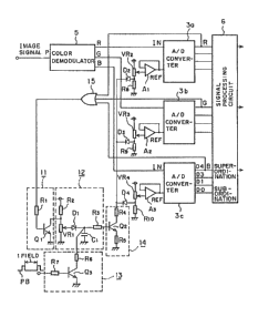
An embodiment of the present invention will be explained
with reference to the accompanying drawings. In Fig. 2, 3a,
3b, 3c designate A/D converters; 5, a color demodulator; 6, a
signal processing circuit; 11, a brightness detector
consisting of a resistor R1 and a transistor Ql to detect
brightness of image signal; 12, an integrator consisting of
~ resistors R2, R3, a capacitor Cl, a diode Dl and a variable
15 resistor VR1; 13, a discharge circuit by a blanking pulse PB
consisting of resistors R6, R7 and a transistor Q3; 14, a
voltage dividing circuit consisting of resistors R4, R5 and a
transistor Q2; R8, R9, R10, voltage dividing resistors; VR2,
VR3, VR4, voltage dividing variable resistors; Al,
. ..
- 4 -
.,
, ' .
, .
1 327855
A2, A3, reference voltage output amplifiers; 15, OR gate
for logical OR of the most significant bits of the A/D
converters 3a, 3b, 3c; D2, D3, D4, reverse current
shut-off diodes.
Operations will be explained below. An image signal
input to the input terminal P is first separated to
three primary-color signals of R, G, B in the color
demodulator and the primary-color signals are then
supplied to the A/D converters 3a, 3b, 3c. These A/D
converters 3a, 3b, 3c convert the R, G, B signals to
quantized digital signals. The most significant bits of
these digital signals, R, G, B are calculated on logical
OR in the OR gate 15 and then an output at the OR gate
lS is input to the brightness detector 11 for detection
of brightness of image signal. For example, in the case
- of a dark image signal, the most significant bits of ,
digital outputs of the A/D converters 3a, 3b, 3c are all
set to lcw level. Therefore, the transistor Ql turns
OFF. In this case, a capacitor Cl of integrator 12 is
charged with the voltage set by the variable resistor
VRl and th~n a base voltage of transistor Q2 is held to
this voltage during the one field period of the vertical
blanking pulse PB, As a result, the transistor Q2 turns
ON and a voltage determined by the variable resistor VR2,
and resistors R4, R5, R8 is supplied to ~he A/D converter
3a as the reference voltage for example. ~he similar
operations are carried out for the A/D converters 3b, 3c.
.: . -, ,:
.
1 327855
In this case, the resolution of the A/D converters 3a,
3b, 3c virtually increase because the reference voltage
becomes lower. On the other hand, in the case of a
bright image signal, the output of OR gate 15 becomes
high level, the transistor Ql turns ON and the capacitor
Cl is not charged. Accordingly, the transistor Q2 turns
OFF and a voltage determined by the variable resistor
VR2 and voltage dividing resistor R8 is applied to the
A/D converter 3a as the reference voltage input, for
example. The reference voltages of the A/D converters
3a - 3c can take two kinds of values depending on the
quality of image signal input, namely the brightness of
the image signal. If the image is dark, the virtual
contrast can be raised by setting such two kinds of
voltage values to the optimum value and high quality
image can be obtained by preventing the saturated black
image of display screen~
In this embodiment, the A/D converters 3a - 3c of 4
bits are used but the converters are not limited only to
them.
As explained previously, the present invention has
the constitution that the reference voltage of the A/D
converter is controlled with the most significant bit
output signal of the A/D converter and therefore provides
the effect that if an image is dark, the contrast can be
adjusted automatically depending on the level of image
signal, and thereby saturated black image on the display
. .
`:
1 327855
screen can be prevented and clear and optimum display
image can be obtained.
~;:
: -