Note : Les descriptions sont présentées dans la langue officielle dans laquelle elles ont été soumises.
1 ~ 3 ~
TITLE OF THE INVENTION
Superconductive Material
BACKGROUND OF THE IN~ENTION
Field of the Invention
The present invention relates to a novel
superconductive material, and more particularly, it
relates to a superconductive material of ceramics which is
employed for a power product to which a superconducting
magnet is applied, a Josephson device for a computer or an
infrared sensor, etc.
Description of the Prior Art
The most significant property of a superconductive
material is that the same enters a superconductive state
at a higher critical temperature. This is because the
obtained critical temperature decides a cooling medium to
be employed and the range of practical use.
The critical temperature of a conventional
superconductive material has been at about 23 K at the
best, while a cooling medium therefor has been generally
prepared by liquid helium, the temperature of which is
sufficiently lower than the critical temperature.
However, such liquid helium is high-priced, while a
costly vacuum adiabatic vessel has been inevitably
required in order to prevent evaporation thereof.
1 ~3~7i2
It has recently been recognized that a ceramics
material shows a superconducting phenomenon. Such a
material is prepared by an oxide which is in K2NiF4 type
layer perovskite crystal structure generally expressed in
a chemical formula (A1 xBx)2CO4 y. It has been confirmed
that such a material shows a critical temperature of about
40 ~. However, this material still requires a cooling
medium of high-priced liquid helium. On the other hand,
an extremely low-priced cooling medium is prepared by
liquid nitrogen, which has a boiling point température of
77 K. Thus, such low-priced li~uid nitrogen can be
employed in place of li~uid helium for a superconductive
material having a critical temperature of at least 77 K,
to extremely widen the range of practical superconduction.
SUMMARY OF THE INVENTION
An object of the present invention is to provide a
superconductive material which has a critical temperature
higher than 77 K, in such view that a ceramics material
shows a superconducting phenomenon.
The present invention provides a superconductive
material of ceramics which is in composition generally
expressed in a formula Aasbcc, where a, b and c are so
selected as to satisfy a relational expression ax (mix
valence of A) + bx (mix valence of B) = cx (mix valence of
C), _ represents at least a single sort of element
selected from those belonging to the groups Ia, IIa and
IIIa of the periodic table, B represents at least a single
sort of element selected from those belonging to the
groups Ib, IIb and IIIb of the periodic table, and C
represents at least either oxygen or fluorine.
The elements belonging to the group Ia of the
periodic table are H, Li, Na, K, Rb, Cs and Fr. The
elements belonging to the group IIa of the periodic table
are Be, Mg, Ca, Sr, Ba and Ra. The elements belonging to
the group IIIa of the periodic table are Sc, Y, La, Ce,
Pr, Nd, Pm, Sm, Eu, Gd, Tb, Dy, Ho, Er, Tm, Yb, Lu, Ac,
Th, Pa, U, Np, Pu, Am, Cm, Bk, Cf, Es, Fm~ Md, No and Lr.
The elements belonging to the group Ib of the
periodic table are Cu, Ag and Au. The elements belonging
to the group IIb of the periodic table are Zn, Cd and Hg.
The elements belonging to the group IIIb of the periodic
table are B, Al, Ga, In and Tl.
A superconductive material obtained according to the
present invention is expressed in the aforementioned
general formula. Such a ceramics superconductive material
can be obtained by a powder sintering method of sintering
powder which is mixed to be in prescribed composition, for
example. Alternatively, the inventive material can be
formed as a thin film by sputtering or CVD.
7 :L 2
It has been confirmed that the superconductive
material obtained in the aforementioned manner is in layer
perovskite structure, and has a high critical temperature
which cannot be obtained by a conventional metal
superconductive material such as niobium-titanium alloy or
niobium-tin alloy.
It has been also confirmed that the superconductive
material obtained according to the present invention shows
a high critical temperature exceeding the boiling point
temperature of 77 K of liquid nitrogen.
Further, it is recognized that a most preferable
superconductive material showing high critical current is
obtained when C in the above chemical formula is expressed
as follows:
C = (Ol_zFz) ~O < z < 0.5]
where O represents oxygen and F represents fluorine.
If the value z exceeds 0.5, fluorine is larger in
amount than oxygen. Thus, a larger number of electrons
contributing to current are captured by fluorine, to
reduce the critical current.
As hereinabove described, a cooling medium can be
prepared by liquid nitrogen by employing the inventive
superconductive material. Thus, the cost for the cooling
medium can be reduced to about 1120, while adiabatic
structure for a cryovessel is simplified, leading to
13 ~ 9
overall reduction in cost for an apparatus utilizing a
superconducting phenomenon.
The present invention is effectively applied to a
Josephson computer device through the high-speed property
of such an effect, and an infrared sensor of high
sensitivity.
These and other objects, features, aspects and
advantages of the present invention will become more
apparent from the following detailed description of the
present invention when taken in conjunction with the
accompanying drawings.
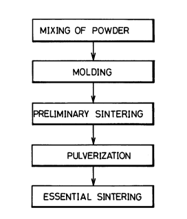
BRIEF DESCRIPTION OF THE DRAWINGS
Fig. 1 is a process drawing showing a powder
sintering method for obtaining a superconductive material
according to the present invention; and
Fig. 2 illustrates electric resistance temperature
dependency of the superconductive material according to
the present invention.
DESCRIPTION OF THE PREFERRED EMBODIMENTS
Example 1
Y203, BaCO3, CuO and CuF2 were employed as raw
materials and sintered by a general powder sintering
method in accordance with steps as shown in Fig. 1. The
mixing ratio was Y203:BaCO3:(CuO+CuF2) = 1:4:6, CuO:CuF2 =
1:0.1 in mole ratio. Preliminary sintering was performed
7 1 ~
at a temperature of 900~C for 10 hours. Then essential
firing was performed on a cylindrical compact of 10 mm in
diameter and 5 mm in thickness at a temperature of 950~C
for two hours.
The cylindrical sample thus obtained was subjected to
measurement of a critical temperature in liquid nitrogen
by a general four-terminal method, to obtain electric
resistance temperature dependency as shown in Fig. 2. As
obvious from Fig. 2, transition from normal conduction to
superconduction started at a temperature of 100 K, and a
superconductive state was attained at a temperature of 91
K. It has been confirmed by measurement that the critical
current was 1100 A/cm2.
Example 2
A target for sputtering was prepared by the
essentially sintered material obtained in Example 1. This
target was employed to perform sputtering in an atmosphere
obtained by supplying fluorine gas into Ar gas. A thin
film could be generated under sputtering conditions of a
substrate temperature of 600~C and Ar gas pressure of 10 1
Torr. Thereafter heat treatment was performed on the thin
film at a temperature of 900~C. As the result of
examination on superconductivity, the thin film as
obtained showed a critical temperature of 85 K.
Further, it has been confirmed through measurement
that critical current density of the thin film was Jc =
150 A/mm .
Example 3
La203, SrC03, CuO and CuF2 were employed as raw
materials and sintered by a general powder sintering
method in accordance with steps as shown in Fig. 1. The
mixing ratio was La203:SrC03:(CuO+CuF2) = 1.85:0.15:1,
CuO:CuF2 = 1:0.1 in mole ratio. Preliminary sintering was
performed at a temperature of 900~C for 10 hours. Then
essential firing was performed on a cylindrical compact of
10 mm in diameter and 5 mm in thickness at a temperature
of 950~C for two hours.
The cylindrical sample thus obtained was subjected to
measurement of a critical temperature in liquid nitrogen
by a general four-terminal method, to obtain electric
resistance temperature dependency as shown in Fig. 2. As
obvious from Fig. 2, transition from normal conduction to
superconduction started at a temperature of 35 K, and a
superconductive state was attained at a temperature of 32
K. It has been confirmed by measurement that the critical
current was llOO A/cm2.
Although the present invention has been described and
illustrated in detail, it is clearly understood that the
same is by way of illustration and example only and is not
~.397 12
to be taken by way of limitation, the spirit and scope of
the present invention being limited only by the terms of
the appended claims.
-- 8