Sélection de la langue

Search

Sommaire du brevet 2000525 

Énoncé de désistement de responsabilité concernant l'information provenant de tiers

Une partie des informations de ce site Web a été fournie par des sources externes. Le gouvernement du Canada n'assume aucune responsabilité concernant la précision, l'actualité ou la fiabilité des informations fournies par les sources externes. Les utilisateurs qui désirent employer cette information devraient consulter directement la source des informations. Le contenu fourni par les sources externes n'est pas assujetti aux exigences sur les langues officielles, la protection des renseignements personnels et l'accessibilité.

Disponibilité de l'Abrégé et des Revendications

L'apparition de différences dans le texte et l'image des Revendications et de l'Abrégé dépend du moment auquel le document est publié. Les textes des Revendications et de l'Abrégé sont affichés :

  • lorsque la demande peut être examinée par le public;
  • lorsque le brevet est émis (délivrance).
(12) Brevet: (11) CA 2000525
(54) Titre français: DISPOSITIF SUPER-LUMINESCENT A EMISSION DE SURFACE, COUPLE A UN RESEAU DE DIFFRACTION
(54) Titre anglais: GRATING-COUPLED SURFACE-EMITTING SUPERLUMINESCENT DEVICE
Statut: Périmé
Données bibliographiques
(52) Classification canadienne des brevets (CCB):
  • 345/46
  • 345/50
(51) Classification internationale des brevets (CIB):
  • H01L 33/60 (2010.01)
  • H01L 33/64 (2010.01)
  • H04B 10/25 (2013.01)
  • G01C 19/64 (2006.01)
(72) Inventeurs :
  • EVANS, GARY ALAN (Etats-Unis d'Amérique)
  • CARLSON, NILS WILLIAM (Etats-Unis d'Amérique)
(73) Titulaires :
  • GENERAL ELECTRIC COMPANY (Non disponible)
(71) Demandeurs :
(74) Agent: CRAIG WILSON AND COMPANY
(74) Co-agent:
(45) Délivré: 1994-05-10
(22) Date de dépôt: 1989-10-12
(41) Mise à la disponibilité du public: 1990-04-27
Requête d'examen: 1992-11-12
Licence disponible: S.O.
(25) Langue des documents déposés: Anglais

Traité de coopération en matière de brevets (PCT): Non

(30) Données de priorité de la demande:
Numéro de la demande Pays / territoire Date
263,464 Etats-Unis d'Amérique 1988-10-27

Abrégés

Abrégé anglais


A GRATING-COUPLED SURFACE-EMITTING
SUPERLUMINESCENT DEVICE
Abstract of the Disclosure
A superluminescent diode has one end coupled to a grating
output coupler and the other end has a reflective coating. A broad light
spectrum is emitted for reduced speckle interference and phase noise
when used in applications such as a gyroscope. The diode can be of
the "P side down" type for good heat dissipation during continuous wave
operation. Two gratings can be used in order to reduce beam
divergence.

Revendications

Note : Les revendications sont présentées dans la langue officielle dans laquelle elles ont été soumises.


- 5 -

The embodiments of the invention in which an exclusive
property or privilege is claimed are defined as follows:
1. A device comprising:
a superluminescent diode having a pair of ends;
a reflecting coating disposed at one of said ends; and
a grating output coupler having a first grating optically
coupled to the other end.
2. The device of claim 1 wherein light is emitted directly
from said grating.
3. The device of claim 1 wherein light is emitted directly
from said diode.
4. The device of claim 1 wherein said diode is of the
DH-LOC type.
5. The device of claim 1 wherein said diode is of the QW
type.
6. The device of claim 1 wherein said grating is blazed.
7. The device of claim 1 further comprising a heat sink
coupled to said diode.
8. The device of claim 1 further comprising a second grating
optically coupled to said first grating.
9. The device of claim 8 wherein said gratings are in
parallel and extend perpendicular to emitted light.
10. The device of claim 9 further comprising a waveguide
optically coupled to said diode and having an effective index of
refraction and a layer disposed over said second grating and having a
higher index of refraction than said waveguide.
11. The device of claim 1 wherein said diode comprises an
optical waveguide having an active length of L and a width of W and

Image

wherein .lambda. = wavelength of light in free space, d = grating period, and
ne = effective index of refraction of said optical waveguide.

Description

Note : Les descriptions sont présentées dans la langue officielle dans laquelle elles ont été soumises.


20005~


-1 - RCA 83,243
A GRATING-COUPLED SURFACE-EMITTING
SUPERLUMINESCENT DEVICE

Backaround of the Invention
The present invention relates to superluminescent (SL)
devices, and more particularly, to such devices that are coupled to
gratings.
Superluminescent devices, such as diodes are less
coherent (broader bandwidth) than laser diodes, and therefore, have
less speckle interference patterns that are random in time. For certain
applications, such as gyroscopes, this is desirable, since the gyroscope
output signal represents a phase difference and any random
interference patterns result in phase noise in the output signal. SL
devices normally have two ends with a reflecting and antireflecting
coatings respectively disposed on the ends. The light is emitted by the
end with the antireflecting co~ting. However, some small amount of
light will be reflected from the antireflecting coating resulting in speckle
interference patterns, and thus, phase noise in a gyroscope output
signal, although less than that when a laser, which has two reflecting
coatings, is used therein.
It is, therefore, desirable to have an SL device which has
reduced speckle interference patterns, and thus, produces reduced
phase noise when used in an application such as a gyroscope.

Summarv of the Invention
A device in accordance with the invention comprises a
superlurninescent diode having a pair of ends; a reflecting coating
disposed at one of said ends; and a grating output coupler having a first
grating optically coupled to the other end to reduce speckle interference
patterns.


~'


'''' ~ , ~ '

2000~25
- 2 - RCA 83,243
Brief Description of the Drawin~s
FIGURE 1 is a side view of a first embodiment af the
invention;
FIGURE 2 is a side view of a second embodiment of the
invention; and
FIGURE 3 shows a side view of a third embodiment of the
invention with reduced beam divergence.

Detailed Description of the Preferred Embodiments
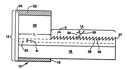
As shown in FIGURE 1, a device in accordance with the
invention, generally designated 10, comprises an SL diode 12, and a
grating output coupler 14. In turn, the SL diode 12 comprises an N-
contact 16, e.g., such as sintered Ni/Ge/Au, a substrate 18, such as
GaAs, an intermediate layer section 20, and a P-ccntact 22 As known
in the art, the section 20 actually comprises a plurality of layers. Details
of the section 20 and the contacts 16 and 22 are the same as for the
corresponding elements of a laser diode such as are shown in
Canadian Application Serial No. 606,257, filed July 20,1989, in the
name of D. Carlin, and entitled "Surface emitting Lasers With Combined
Output". Most importantly, the section 20 comprises an optlcal
waveguide 23 having an active length "L" and a width "W". Typically
"W" is between about 1 to 4 m and "L" is between about 100 to 500 m.
A reflective coating 24, e.g., such as shown in U.S. Patent No.
4,092,659, is disposed at one end of the SL diode 12. As shown in said
U.S. patent, the coating 24 preferably comprises 3 pairs of
alternate layers of Al203 and S02, each layer being one-quarter
wavelength thick for a total of 6 layers. The grating output couples 14 is
optically coupled to the other end of the diode 12 and has a grating 27
that is formed in part of a P-cladding layer (not shown) of the waveguide
23 of the section 20, if the SL diode 12 is of the quantum wall (QW)
type, or the grating 27 is part of the waveguide 23 of the section 20, if
the diode 12 is of the double heterostructure-large optical cavity
(DH-LOC) type. Both types are shown in aforementioned Canadian
Application Serial No. 606,257.
The first order of the second order grating output coupler 14
is used, which provides light at an angle ~ to the normal 25 Q the layer
20 as shown by the arrow 26. The angle ~ ~ arc sin ~ ne
d


,

. , - , -
.
- ` ~- :- ' ' ,.
' - ' . . ' .::

-~ 2000~2~
- 3 - RCA 83,243

wherein ~ = wavelength of light in free space, d = grating period, and
ne = effective index of refraction of the waveguide 23 in the layer 20.
preferably, in order to maximize the emitted light, the grating 27 is
blazed in the first order, e.g., the grating portion 28 is typically at a 45
degree angle to said normal 25, although other angles for the blazing
can be used, while grating portion 30 is parallel to said normal. The
grating period "d" is selected so that only single pass gain occurs, this
can be done by satisfying the inequality arc sin ~ -; >> W
c _ ned L.
The spacing "d" typically is between about 2500A to 3500A
(Angstroms). Details about blazed gratings are found in the article
"Simplified approach to surface-wave scattering by blazed dielectric
gratings", by K.C. Chang et al., Applied Optics, Vol. 19, No. 2, January
15, 1980, pages 282-288.
In operation, positive and negative voltages are applied to
the contacts 22 and 16, respectively, and then stimulated emission of
photons occurs in the SL diode 12. since only one reflective coating 24
is present and the above inequality is satisfied, only single pass gain
occurs in the SL diode 12. Thus, relatively broad spectrum light is
emitted by the SL diode 12 and then coupled out after said single pass
directly from the grating output coupler 14. There are no Fabry-Perot
modes in the present invention, compared with an SL diode having both
reflecting and antireflecting coatings that can give rise to residual Fabry-
Perot modes. Therefore, there will be reduced speckle interference
patterns, and hence phase noise, when used in an application, e.g.,
such as a gyroscope.
in the second embodiment of FIGURE 2, the so called "P
side down" type, and wherein corresponding elements have
corresponding reference numerals, there is a heat sink 32, e.g., Cu,
typically of at least 2 mils (0.005 cm) thickness. A contact 34, e.g., Au,
between about 1 000-2500A thick is on the sink 32. In contradistinction
to FIGUR~ 1, the P-contact 22 is below the intermediate layer section
20 while the N-contact 16 is thereabove. The grating output coupler 14
is below some of the layers of the section 20, e.g., the waveguide 23 is
the SL diode 12 is of the DH-LOC type or the quantum well and


,,

~:; - . . : - ..
; . : .


,

- ,. .

2000~25
- 4 - RCA 83,242

confining layers (not shown) if the SL diode 12 is of the QW type. A
coating 36 can be highly reflecting and made as explained above for
coating 24 or be partially reflecting, e.g., a layer of Si3N4 The light 26
emerges perpendicular to the longitudinal direction of the grating output
5 coupler 14 and directly from the diode 12, in particular, from the
intermediate layer section 20 thereof.
The above embodiment has the active layer (DH-LOC type)
or quanturn well (QW type) close to the heat sink 32 for good heat
dissipation, and therefore, good operation in the continuous wave mode
10 is achieved.
In FIGURE 3, a transparent layer 38, which has a difference
index of refraction than the grating output coupler 14 and a typical
thickness between about 1-2,um, overlies the grating output coupler 14.
The layer 38 can comprise AlGaAs, SiO2, Si3N4, etc. A second grating
15 40 (first or second order) is at the top of the layer 38, with its
longitudinal direction parallel to that of grating output coupler 14. The
grating 40 can have a different blazing than that of grating 27.
Overlying the grating 40 is a layer 42. The condition for outcoupling
light from layer 42 is that its index of refraction is greater than that of the
20 waveguide 23. Layer 42 must be sufficiently thin so that the outcoupled
light is not absorbed. About 100A thickness of InSb can be used as well
as other materials. The light 26 emerges perpendicularly or some other
angle from the grating 40. The embodiment of FIGURE 3 has a beam
divergence of only about one degree or less for all wavelengths
25 compared to a divergence between about 2-3 degrees for the
embodiments of FIGURES 1 and 2 for a grating output coupler length
between about 200-300~m. ,


.- . - , ,

~,
,
~ . '- , :

.. . . . . .

Dessin représentatif
Une figure unique qui représente un dessin illustrant l'invention.
États administratifs

Pour une meilleure compréhension de l'état de la demande ou brevet qui figure sur cette page, la rubrique Mise en garde , et les descriptions de Brevet , États administratifs , Taxes périodiques et Historique des paiements devraient être consultées.

États administratifs

Titre Date
Date de délivrance prévu 1994-05-10
(22) Dépôt 1989-10-12
(41) Mise à la disponibilité du public 1990-04-27
Requête d'examen 1992-11-12
(45) Délivré 1994-05-10
Expiré 2009-10-12

Historique d'abandonnement

Il n'y a pas d'historique d'abandonnement

Historique des paiements

Type de taxes Anniversaire Échéance Montant payé Date payée
Le dépôt d'une demande de brevet 0,00 $ 1989-10-12
Enregistrement de documents 0,00 $ 1990-05-25
Taxe de maintien en état - Demande - nouvelle loi 2 1991-10-14 100,00 $ 1991-09-19
Taxe de maintien en état - Demande - nouvelle loi 3 1992-10-12 100,00 $ 1992-09-03
Taxe de maintien en état - Demande - nouvelle loi 4 1993-10-12 100,00 $ 1993-09-16
Taxe de maintien en état - brevet - nouvelle loi 5 1994-10-12 150,00 $ 1994-08-23
Taxe de maintien en état - brevet - nouvelle loi 6 1995-10-12 150,00 $ 1995-08-29
Taxe de maintien en état - brevet - nouvelle loi 7 1996-10-14 150,00 $ 1996-08-28
Taxe de maintien en état - brevet - nouvelle loi 8 1997-10-14 150,00 $ 1997-08-29
Taxe de maintien en état - brevet - nouvelle loi 9 1998-10-13 150,00 $ 1998-08-31
Taxe de maintien en état - brevet - nouvelle loi 10 1999-10-12 200,00 $ 1999-08-30
Taxe de maintien en état - brevet - nouvelle loi 11 2000-10-12 200,00 $ 2000-09-21
Taxe de maintien en état - brevet - nouvelle loi 12 2001-10-12 200,00 $ 2001-09-21
Taxe de maintien en état - brevet - nouvelle loi 13 2002-10-14 200,00 $ 2002-09-19
Taxe de maintien en état - brevet - nouvelle loi 14 2003-10-13 200,00 $ 2003-09-22
Taxe de maintien en état - brevet - nouvelle loi 15 2004-10-12 450,00 $ 2004-09-21
Taxe de maintien en état - brevet - nouvelle loi 16 2005-10-12 450,00 $ 2005-09-21
Taxe de maintien en état - brevet - nouvelle loi 17 2006-10-12 450,00 $ 2006-09-18
Taxe de maintien en état - brevet - nouvelle loi 18 2007-10-12 450,00 $ 2007-09-17
Taxe de maintien en état - brevet - nouvelle loi 19 2008-10-13 450,00 $ 2008-09-17
Titulaires au dossier

Les titulaires actuels et antérieures au dossier sont affichés en ordre alphabétique.

Titulaires actuels au dossier
GENERAL ELECTRIC COMPANY
Titulaires antérieures au dossier
CARLSON, NILS WILLIAM
EVANS, GARY ALAN
Les propriétaires antérieurs qui ne figurent pas dans la liste des « Propriétaires au dossier » apparaîtront dans d'autres documents au dossier.
Documents

Pour visionner les fichiers sélectionnés, entrer le code reCAPTCHA :


Pour visualiser une image, cliquer sur un lien dans la colonne description du document. Pour télécharger l'image (les images), cliquer l'une ou plusieurs cases à cocher dans la première colonne et ensuite cliquer sur le bouton "Télécharger sélection en format PDF (archive Zip)" ou le bouton "Télécharger sélection (en un fichier PDF fusionné)".

Liste des documents de brevet publiés et non publiés sur la BDBC .

Si vous avez des difficultés à accéder au contenu, veuillez communiquer avec le Centre de services à la clientèle au 1-866-997-1936, ou envoyer un courriel au Centre de service à la clientèle de l'OPIC.


Description du
Document 
Date
(yyyy-mm-dd) 
Nombre de pages   Taille de l'image (Ko) 
Page couverture 1994-07-16 1 30
Abrégé 1994-07-16 1 17
Revendications 1994-07-16 1 40
Dessins 1994-07-16 2 51
Description 1994-07-16 4 200
Correspondance de la poursuite 1992-11-12 2 61
Demande d'examen 1993-03-02 1 70
Correspondance de la poursuite 1993-05-13 2 63
Correspondance reliée au PCT 1994-02-17 1 31
Lettre du bureau 1992-12-21 1 41
Correspondance reliée au PCT 1990-06-07 1 25
Lettre du bureau 1990-05-28 1 15
Taxes 1991-09-19 2 70
Taxes 1992-09-03 1 39
Taxes 1996-08-28 1 54
Taxes 1995-08-29 1 42
Taxes 1994-08-23 1 57
Taxes 1993-09-16 1 39