Note : Les descriptions sont présentées dans la langue officielle dans laquelle elles ont été soumises.
200~90
71180-105
Backqround of the Invention
The present inventlon relate~ to a decoder in a radlo
paging receiver and, more particularly, to a preamble detector
which can detect a preamble in a radio paging signal within a
short period of time.
Brief DescriPtion of the Drawinqs
Fig. 1 is a block diagram of a preamble detector
according to an embodiment of the present invention;
Fig. 2 is a block diagram of a conventional paging
receiver to which the present invention is applied;
Fig. 3 is a block diagram of a decoder of a paging
receiver to which the present invention is applied;
Fig. 4 is a block diagram of a conventional preamble
detector;
Fig. 5A shows timing charts for explaining the operation
of the decoder of the conventional paging receiver;
Figs. 5B and 5C show timing charts for explaining the
operation of a decoder of the paging receiver according to the
embodiment of the present invention;
Fig. 6 shows a format of a paging signal (CCIR No. 1
code);
Fig. 7A shows timing charts for explaining the operation
of the conventional preamble detector;
Fig. 7B shows timing charts for explaining the operation
of the preamble detector according to the present invention;
Fig. 8 is a block diagram of a preamble detector
accordlng to another embodiment of the present invention;
.~., 1 .
2~,0~90
71180-105
Fig. 9 ls a circult diagram of a second preamble
detection circuit shown in Flg. 8;
Fig. 10 is a circuit dlagram of an error counter shown
in Fig. 9;
Fig. 11 is a circuit diagram of a reception controller
shown in Fig. 3; and
Fig. 12 is a state transition diagram of the three modes
of a controller.
A conventional radio paging receiver comprises a
receivlng section 201, a decoder section 202, and an alert
generator 203, as shown in Fig. 2. The receiving section 201 is
intermittently operated in response to a battery saving control
signal CONT to reduce power consumption. The decoder section 202
processes received data DATA demodulated by the receiving section
201. When the decoder section 202 detects an address of its own
receiver from the received data DATA, it outputs an address
detection pulse ADET. The alert generator 203 performs an alert
operation using a speaker, an LED, and the like in response to the
address detection pulse ADET.
The format of a paging signal consists of a preamble
(PA) comprising a repetitive pattern of "1" and "O" signals, and a
plurality of batches which follow the preamble, as shown in Eig.
6, as recommended in, e.g., the CCIR (CCIR RPC No. 1, also called
a POCSAG code). One batch includes one synchronization signal
(SC) and eight
l~ 2
X00~5~
frames. An address signal is sent as a codeword in a
predetermined frame.
In order to receive the paging signal described
above, the decoder section 202 (Fig. 2) comprises a bit
synchronization circuit 301, a preamble detector 302, a
synchronization signal detector 303, an address detector
304, and a reception controller 305, as shown in Fig. 3.
The conventional preamble detector comprises a
shift register consisting of D flip-flops 401 to 404, and
an AND gate 406, as shown in Fig. 4. More specifically,
the preamble detector samples the received data DATA in one
phase of a clock CLK extracted by the bit synchronization
circuit 301 (Fig. 3) to perform a preamble detection
operation.
The operation of the decoder section 202 (Fig. 2)
of the conventional paging receiver will be described
below. The operation of the decoder section can be
classified into three states, i.e., a preamble search mode,
a synchronization signal search mode, and an address search
mode.
Referring to Fig. 5A, in the preamble (PA) search
mode, the receiving section is cyclically turned on (CONT =
"1"). At this time, the bit synchronization circuit 301
and the preamble detector 302 shown in Fig. 3 are enabled
(enable signal BENA = enable signal PAENA = "1"). The bit
synchronization circuit 301 corrects the phase of a clock
to be synchronous with the received signal. The preamble
,~, - 2, -
200~590
detector 302 samples the received data DATA in response to
the clock CLK output from the bit synchronization circuit
301, and checks the presence/absence of the preamble PA.
When the preamble PA is detected IPreamble
detection pulse PADET = "1"), the decoder section 202
(Fig. 2) enters the synchronization signal (SC) search
mode. At this time, the reception controller 305 causes
the receiving section 201 (Fig. 2) to continuously operate,
and enables the synchronization signal detector 303 (enable
signal SCENA = "1"). When the synchronization signal
detector 303 detects the synchronization signal
(synchronization signal detection pulse SCDET = "1"), frame
synchronization is established, and the decoder section 202
enters the address search mode.
In the address search mode, the reception
controller 305 causes the receiving section 201 to
intermittently operate at timings of frames assigned to its
own receiver, and enables the address detector 304 (enable
signal AENA = "1"). The bit synchronization circuit 301 is
enabled when the receiving section 201 is set ON even in
the addre~s search mode so as not to miss bit
synchronization during long data. In this case, a time
constant for clock phase correction is normally set to be
large so as to prevent clock phase disturbance caused by
noise (BMODE = "0"). When the address detector 304 detects
an address assigned to the receiver, it outputs an address
detection pulse (ADET = "1"). In response to the address
~.,'",~''' ~
200~59C~
detection pulse, the alert generator 203 (Fig. 2) i8
enabled, to make the speaker, the LED, and the like
operate, thus alerting the user to detection of paging.
When the synchronization signal cannot be
detected from a predetermined number of (e.g., two)
consecutive paging signals, or when an address code error
is detected from consecutive paging signals, it is
determined that frame synchronization is missed. Thus, the
decoder section is restored to the preamble (PA) search
mode. When the preamble is detected, it is also determined
that frame synchronization is missed, and the decoder
section is restored to the synchronization signal (SC)
search mode (U.S.P. No. 4,839,634).
In the decoder section of the conventional radio
lS paging receiver, the preamble detector 302 checks the
preamble PA in only one phase of the clock output from the
bit synchronization circuit 301. Therefore, in the
preamble search mode, the decoder section first performs a
bit synchronizing operation, and detects a preamble after
bit synchronization is established. Therefore, it ta~es
much time until the preamble is detected. In other words,
when the receiving section is intermittently operated, the
ON time of the receiver (TBS in Fig. 5A) must be increased
by a time period necessary for bit synchronization,
resulting in poor battery saving efficiency.
As shown in Fig. 5A, when data bursts are
consecutively supplied at short intervals (Tl batch
~c ~
.. '`` ~
2~0~590
71180-lOS
length in Fig. 5A), the two bursts normally have dlfferent bit
phases. For this reason, the conventional preamble detector shown
in Fig. 4 may fail to recelve the preamble of the second data
burst when the duty ratio of the preamble is offset from 50% due
to an offset of characteristics of the receiving section, as shown
in Fig. 7A. In this case, an address (A3) included in the second
burst shown in Fig. 5A cannot often be received.
Summarv of the Invention
It is therefore an object of the present invention to
provide a radio paging receiver which can improve battery saving
efficiency.
It is another object of the present invention to provide
a radio paging receiver which can reliably receive consecutive
data bursts.
According to the present invention, there is provided a
radio paging receiver which comprises a receiving section for
intermittently receiving a paging signal including a preamble
signal, a synchronization signal, and an address signal, a decoder
section for processing a signal demodulated by the receiving
section, and an alert generator for generating an alert siqnal in
response to the detection of an address signal assigned to the
receiver, the decoder section including: bit synchronization means
for producing a clock synchronized with a received signal;
preamble detection means for detecting the preamble signal and
outputting a preamble detection signal said preamble detection
means checking the preamble signal in at least two different
phases of one period of sald clock; synchronization signal
2004S90
71180-105
detection means for detectlng the synchronlzation slgnal and
outputting a synchronization slgnal detection signal; addresx
signal detection means for detecting the address signal assigned
to the receiver and outputting an address detection signal; and
reception control means responsive to the preamble detection
signal and the synchronization signal detection signal for
outputting a battery saving control signal controlling an
intermittent reception operation of the receiver and a control
signal controlling the bit synchronization means, the preamble
detection means, the synchronization signal detection means, and
the address detection means.
DescriPtion of the Preferred Embodiments
The first embodiment of the present invention will now
be described in detail with reference to the accompanying
drawings.
200~
A radio paging receiver according to the pre~ent
invention has the same arrangement as that shown in Fig. 2,
and a decoder section as the principal part of the present
invention has substantially the same arrangement as ~hown
in Fig. 3.
However, a preamble detector according to the
present invention has a quite different arrangement from
that of the preamble detector shown in Fig. 3, as will be
described later.
For these reasons, the embodiment of the present
invention will be described below with reference to not
only Fig. 1 but also Figs. 2 and 3.
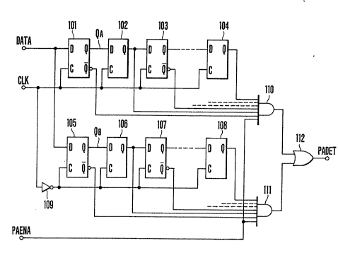
The preamble detector according to this
embodiment comprises a first shift register consisting of D
flip-flops 101 to 104, a second shift register consisting
of D flip-flops 105 to 108, AND gates 110 and 111, and an
OR gate 112. More specifically, the preamble detector
according to this embodiment has a circuit for sampling
received data in a phase different by 180 from a clock CLK
extracted by a bit synchronization circuit (Fig. 3) to
perform a preamble detection operation in addition to the
conventional preamble detector for sampling received data
in one phase of the clock CLK extracted by the bit
synchronization circuit 301. When the preamble detector
detects a preamble in one of these phases, it outputs a
preamble detection pulse ~PADET).
- 8 -
~00~5~0
The operation of the decoder section of the
paging receiver according to this embodiment of the pre~ent
invention will be described below. The operation of the
decoder section can be classified into three states, i.e.,
a preamble search mode, a synchronization signal search
mode, and an address search mode.
Referring to Fig. 5B, in the preamble search
mode, a receiving section 201 is cyclically turned on
(battery saving control signal CONT = "1"). At this time,
the bit synchronization circuit 301 and the preamble
detector 302 are enabled (enable signal BENA = enable
signal PAENA = "1").
The ON time (T~s) of the receiving section 201
can be set to be shorter than the ON time (TBs') of the
receiving section in the conventional receiver
(TBS TBS'). The bit synchronization circuit 301 corrects
the phase of the clock CLK to be synchronized with received
data DATA. The preamble detector 302 samples the received
data DATA in two phases of the clock CLK output from the
bit synchronization circuit 301 (at the leading and
trailing edges of the clock CLK) to check the
presence/absence of the preamble.
When the preamble is detected (preamble detection
pulse PADET - "1"), the decoder section 202 enters the
synchronization signal (SC) search mode. At this time, a
reception controller 305 causes the receiving section 201
to continuously operate, and enables a synchronization
200~5i~
signal detector 303 (enable signal SCENA - "1"). When the
synchronization signal detector 303 detects the
synchronization signal ~synchronization signal detection
pulse SCDET = "1"), frame synchronization is established,
and the decoder section 202 enters the address search mode.
In the address search mode, the reception
controller 305 causes the receiving section 201 to be
intermittently operated at timings of frames assigned to
its own receiver, and enables an address receiving circuit
304 (enable signal AENA = "1"). The bit synchronization
circuit 301 is enabled when the receiving section 201 is
set ON so as not to miss bit synchronization during long
data. In this case, the time constant for clock phase
correction is normally set to be large so as to prevent
phase disturbance caused by noise (BMODE = "0"). When the
address receiving circuit 304 receives the assigned
address, it outputs an address detection pulse (ADET =
"1"). In response to the address detection pulse (ADET),
an alert generator 203 is enabled to operate a speaker, an
LED, and the like, thus alerting the user to detection of
paging.
When the synchronization signal cannot be
detected from a predetermined number of (e.g., two)
consecutive paging signals, or when an address code error
25 i8 detected from consecutive paging signals, it is
determined that frame synchronization is missed. Thus, the
decoder section is restored to the preamble (PA) search
-- 10 --
.
~0~ 5'30
mode. When the preamble is detected, it is also determined
that frame synchronization is mis6ed, and the decoder
section is restored to the synchronization signal ~SC)
search mode.
Referring to Fig. 7B, first and second data
bursts are consecutively sent, and have different bit
synchronization timings. When the duty ratio of the
preamble is offset by offset characteristics of the
receiving section, in the preamble detector of the present
invention, the shift register fetches all "O"s like in the
conventional receiver at the leading edge of the clock, and
cannot detect the preamble. However, the shift register
which samples data at the trailing edge of the clock can
correctly fetch "1", "0",..., data, and can detect the
preamble (PADET = 1). As described above, when the
preamble is detected in the address search mode, the
decoder section enters the synchronization signal search
mode. Therefore, as shown in Fig. 5B, correct
synchronization can also be established for the second
burst. Therefore, an address ~A3) included in the second
data burst can be reliably detected unlike in the
conventional decoder section.
As described above, in a decoder section of the
radio paging receiver according to the first embodiment of
the present invention, the preamble detector checks a
preamble in a plurality of phases of a clock extracted by
the bit synchronization circuit. When the preamble is
-- 11 --
2()0~5~ 0
detected in at least one phase, the preamble detector
outputs the preamble detection pulse, and can detect the
preamble even if bit synchronization iB not established.
Thus, battery saving efficiency can be improved, and
consecutively input data bursts can be reliably received.
The second embodiment of the present invention
will be described below with reference to Figs. 8 to 10.
In this embodiment, the preamble detector 302 shown in
Fig. 3 is divided into two circuits to check a preamble of
received data in a plurality of phases of a clock.
Fig. 8 shows a preamble detector of the second
embodiment. The preamble detector shown in Fig. 8
comprises first and second preamble detection circuits 302A
and 302B~ and an OR gate 350. In this case, the first
preamble detection circuit 302A has the same arrangement as
the conventional circuit shown in Fig. 4. The second
preamble detection circuit 302B is constituted by a circuit
shown in Fig. 9.
In Fig. 9, reference numerals 501 and 512 denote
D flip-flops; 502 and 503, exclusive OR gates; 504 and 505,
inverters; 510, an OR gate; 511, an AND gate; and 506 to
509, error counters for counting the number of bits
noncoinciding with the preamble. Each of these error
counters 506 to 509 has the arrangement as shown in
Fig. 10.
In Fig. 10, reference numerals 607 and 608 denote
D flip-flops; 605, an exclusive OR gate; 606, an inverter;
- 12 -
X00'~590
602 and 604, OR gates~ 601, 603, 609, and 611, AND gates;
and 610, a NAND gate.
Fig. 10 shows a counter for judging whether or
not an error count is 2 or less. An input terminal ERR
receives "1" when there is an error; "0" when there is no
error. An input terminal RST receives "1" when the error
count stored in the flip-flops 607 and 608 is cleared.
The signals to the terminals ERR and RST are
input in synchronism with a clock input from the input
terminal CK. The flip-flops 607 and 608 store an error
count. The flip-flop 607 indicates the units digit, and
the flip-flop 608 indicates the tens digit.
Every time "1" is input to the terminal ERR, the
flip-flops 607 and 608 are counted up like 0 ~ 2 -~3 by
the gates 601 to 605. Even when "1" is input to the
terminal ERR when the error count = 3, the count "3" is
maintained. Therefore, an output terminal DET outputs "1"
when neither the flip-flops 608 nor 607 indicate "1" (error
count of 3 or more), i.e., when the error count is 2 or
less.
The operation of the circuit shown in Fig. 8 will
be described below. The D flip-flop 512 (Fig. 9) generates
a Q output corresponding to a preamble pattern (0101...) on
the basis of a clock CLK. The exclusive OR gate 502
compares received data DATA with the preamble pattern
generated by the D flip-flop 512. The error counter 506
counts the number of noncoincidences between the received
- 13 -
20l)~5~
data DAT~ and the preamble pattern (0101...) from the D
flip-flop 512, and outputs a DET pulse when the error count
is equal to or smaller than 2. The error counter 507
counts the number of noncoincidences between the received
data DATA and a pattern (1010...) inverted by the inverter
504, and outputs a DET pulse when the error count is equal
to or smaller than 2 like in the error counter 506. The D
flip-flop 501 fetches the received data DATA at the timing
of the clock CLK, and shifts the received data DATA by a
half-bit time. The exclusi~e OR gate 503 compares the data
shifted by the half-bit time and the preamble pattern
(0101...). For this reason, the exclusive OR gate 503
makes comparison in a phase shifted by 180 from that of
the exclusive OR gate 502. The error counters 508 and 509
respectively count the numbers of noncoincidences of the
half-bit shifted data with the patterns 0101... and 1010...
like in the error counters 506 and 507, and output a DET
pulse when the error count is equal to or smaller than 2
like in the error counter 506.
The gates 510 and 511 output a preamble detection
pulse PADET2 at a timing of PAENA2 = "1" when the count of
any of the error counters 506 to 509 is equal to or smaller
than 2. Note that the gate 511 outputs the pulse PADET2
upon reception of the output from the gate 510 and PAENA2.
Fig. 5C shows timing charts of signals output in
thiq embodiment. With this arrangement, the number of
flip-flops constituting the preamble detector can be
- 14 -
200'~5~-~t)
decreased as compared to the first embodiment shown in
Fig. l.
In this case, since the first preamble detec~ion
circuit 302A has the conventional circuit arrangement, it
operates before the synchronization signal SC is detected,
as can be seen from Fig. 5C, and the second preamble
detection circuit 302B operates after the synchronization
signal SC is detected.
Note that the first preamble detection circuit
302A can check the presence/absence of the preamble for
every bit, and the second preamble detection circuit 302B
can check the presence/absence of the preamble in units of
the number of bits of the address signal.
Fig. 11 shows an arrangement of the reception
controller 305 shown in Fig. 3. In Fig. 11, reference
numeral 701 denotes a modulo 32 counter for counting one
word, i.e., 32 bits; and 702, a modulo 17 counter for
counting one batch, i.e., 17 words.
Reference numerals 705 and 706 denote S-R
flip-flips. These flip-flops 705 and 706 perform an
operation for discriminating three operation modes, i.e.,
the preamble (PA) search mode, the SC search mode, and the
address search mode.
Reference numerals 708 and 709 denote first and
second timers. The first timer 708 outputs a time-out
pulse when the SC cannot be detected within a predetermined
period of time in the SC search mode. The second timer 709
- 15 -
20C~590
outputs a time-out pulse when the SC cannot be received
within a predetermined period of time. Reference numeral
710 denotes a gate circuit. The gate circuit 710 outputs
various control signals in accordance with outputs Ml and
M2 of the flip-flops 705 and 706 and the counts of the
modulo 32 counter 701 and the modulo 17 counter 702
associated with the operation mode at timings shown in
Figs. 5B and 5C.
In the second embodiment described above, the bit
synchronization circuit sets a larger time constant for the
clock phase correction after the synchronization signal is
detected than that before detection.
Fig. 12 is a state transition diagram of the
three operation modes of the controller. More
specifically, in the preamble search mode, the controller
enters the SC search mode in response to the PADET pulse,
and enters the address search mode in response to the SCDET
pulse. In the SC search mode, the controller enters the
address search mode in response to the SCDET pulse, and
enters the preamble search mode in response to the time-out
pulse from the first timer 708. In the address search
mode, the controller enters the SC search mode in response
to the PADET pul~e, and enters the preamble search mode in
response to the time-out pulse from the second timer 709.
Note that a relationship between the modes and
the outputs M1 and M2 from the flip-flops 705 and 706 is
given as follows:
- 16 -
2(~0~ 30
M1 M2
Preamble CP~ Search Mode 0 0
SC Search Mode 1 0
Address Search Mode 0
- 17 -