Note : Les descriptions sont présentées dans la langue officielle dans laquelle elles ont été soumises.
2005~55
-- 1 --
SPECIFICATION
PHOTOSENSOR
TECHNICAL FIELD
This invention relates to an improvement in the
photosensor. More particularly, it relates to an
improvement in the contact photoelectric transducer
which comprises amorphous silicon as the main
component.
BACKGROUND ART
The conventional contact image sensors may be
classified into two types: photoconductor type and
photodiode type. In the photoconductor type image
sensors, their photoconductivity is utilized and a
current proportional to the voltage applied can be
obtained. However, they are disadvantageous in that
the response speed is slow. Accordingly, the photo-
diode type image sensors, in which a layer of ampor-
phous silicon carbide or the like is used as a blocking
layer and in which the rectifying effect of the diode
is utilized so that carriers photoelectrically gene-
rated alone can afford the output current, have become
a focus of attention.
However, while the photodiode type is advantageous
, .
.,
;
. ."
,
.`~'`, , '. ' : . .
.:,,,:
: ~ ` . -` ' `
2005255
in that the bright/dark current ratio is greater as
compared with the photoconductor type, the photodiode
type still has a problem tc be solved. Thus, the
photocurrent intensity is limited to a level lower than
1 when expressed in terms of quantum efficiency.
Accordingly, charge accumulation and amplification, for
instance, are required, presenting difficulties from
the circuit viewpoint.
It is an object of the invention to provide a
photosensor in which the dark current is slight and the
bright curren~ is fairly strong.
DISCLOSURE OF THE INVNETION
The invention provides a photosensor which com-
prises a first electrode layer, a ligth-transmitting
second electrode layer, and a laminate structure
disposed between the two electrode layers and comprisng
a first photoconductive layer, a blocking layer and a
second photoconductive layer for charge injection as a
result of modification of the electrical properties of
the first photoconductive layer and of the blocking
layer, the main component of said first photoconductive
layer being silicon, said blocking layer being made of
a substance having a broader band gap as compared with
hydrogenated amorphous silicon and composed mainly of
silicon and carbon or mainly of silicon and nitrogen or
'"
~,'
;~,.'.' ' .
;~,~''
_ 3 - 2005255
mainly of silicon and oxygen, and the main component of
said second photoconductive layer being silicon doped
with an element(s) of the group III of the periodic
table or an element(s) of the group V of the periodic
table as an impurity(ies). In this photosensor, the
bright current can be increased while the dark current
remains suppressed.
In the above-mentioned photosensor, the magnitude
of charge injection may be controlled by controlling
the impurity level in the second photoconductive layer
within the range of 1 ppm to 10,000 ppm.
In the above-mentioned photosensor, the magnitude
of charge injection may be controlled by adjusting the
thickness of the above-mentioned second photoconductive
layer to a value not less than 20 angstroms but smaller
than 5,000 angstroms.
In the above-mentioned photosensor, the magnitude
of charge injection may be controlled by controlling
the band gap of the above-mentioned blocking layer
within the range of 1.7 eV to 6 eV.
In the above-mentioned photosensor, a substance
having a broader band gap as compared with hydrogenated
amorphous silicon and composed mainly of silicon and
carbon or mainly of silicon and nitrogen or mainly of
silicon and oxygen, in each case doped with an ele-
.. .
:'
, .,
.. i, . . . .
.,
, .................................. .
~ ~,`; ., ' '
... .
: ' ' .
_ 4 _ 2005255
ment(s) of the group III of the periodic table or anelement(s) of the group V of the periodic table as an
impurity(ies) may be used as the above-mentioned
blocking layer.
In the above-mentioned photosensor, the magnitude
of charge injection may be controlled by controlling
the impurity level in the blocking layer within the
range of 0 ppm to 10,000 ppm.
In the above-mentioned photosensor, the magnitude
of charge injection may be controlled by adjusting the
thickness of the blocking layer to a value not less
than 20 angstroms but smaller than 5,000 angstroms.
BRIEF DESCRIPTION OF THE DRAWINGS
Fig. 1 to Fig. 5 show, in cross section, various
examples of the photosensor according to the invention,
and
Fig. 6 (a), (b) and (c) graphically show the
voltage-current characteristics, on light irradiation
and in the dark, of a sensor for comparison and two
examples of the sensor shown in Fig. 5.
BEST MODES FOR CARRYING OUT THE INVENTION
Example 1
The structure of one of the embodiments of the
invention is shown in Fig. 1. A transparent conductive
layer is formed as the second electrode layer 2 on a
.
., .
. ~ - , ' .
, . .
., .
- 5 _ 2005255
transparent insulator substrate 1. A thin film having
an energy band gap of 1.7 eV to 6 eV, preferably 1. 8 eV
to 2.8 eV, and composed mainly of silicon and carbon or
mainly of silicon and nitrogen or mainly of silicon and
oxygen, in each case doped with 0 ppm to 10,000 ppm,
preferably 2 ppm to 5,000 ppm, of an element(s) of the
group III of the periodic table or an element(s) of the
group V of the periodic table as an impurity(ies) is
formed as the blocking layer 3 on said second electrode
layer 2. The blocking layer 3 has a tickness not less
than 20 angstroms but less than 5,000 angstroms,
preferably not less than 50 angstroms and not more than
2,000 angstroms. When the layer 3 is thinner than 20
angstroms, blocking cannot be sufficient. When the
layer thickness exceeds 5,000 angstroms, the sensiti-
vity tends to decrease markedly. Furthermore, on said
layer 3, there is formed, as the impurity-containing
photoconductive layer 4, a thin film of hydrogenated
amorphous silicon doped with 1 ppm to 10,000 ppm of an
element(s) of the group III or V of the periodic table
as an impurity(ies). The impurity addition level is
preferably 2 ppm to 5,000 ppm. Its thickness is not
less than 20 angstroms but less than 5,000 angstroms,
preferably 50 to 2,000 angstroms. On the layer 4, a
thin film of impurity-free hydrogenated amorphous
:',;
.~.
~, .
- 6 - 2005255
silicon is formed as the photoconductive layer S. An
electrode layer is further formed thereon as the
metal-made first electrode layer 6. This electrode is
made of one of the materials Cr, Al, Zr, Ti, Ni and W
or an alloy or laminate structure composed of two or
more of these materials. An n-type semiconductor layer
can be inserted between the photoconductive layer and
metal so that the metal and semiconductor layer may
have the ohmic characteristic.
Example 2
The structure of another embodiment of the inven-
tion is illustrated in Fig. 2. On a transparent
insulator substrate 1, a transparent conductive film is
formed as the second electrode layer 2. On the layer
2, a thin film having an energy band gap of 1.7 eV to 6
eV, preferably 1.8 eV to 2.8 eV, and composed mainly of
silicon and carbon or mainly of silicon and nitrogen or
mainly of silicon and oxygen, in each case doped with 0
ppm to 10,000 ppm, preferably 2 ppm to 5,000 ppm of an
element(s) of the group III or V of the periodic table
is formed as the blocking layer ~. The blocking layer
has a thickness not less than 20 angstroms but less
than 5,000 angstroms, preferably a thickness of 50
angstroms to 2,000 angstroms. Further thereon, a thin
film of hydrogenated amorphous silicon doped with 1 ppm
, - ' .
. .
. ~
.~: , .,
:
,:
~, .
~ 7 ~ 2005255
to 10,000 ppm, preferably 2 ppm to 5,000 ppm, of an
element(s) of the group III or V of the periodic table
is formed as the impurity-containing photoconductive
layer 4. Its thickness is not less than 20 angstroms
but does not exceed 5,000 angstroms, preferably 50 to
2,000 angstorms. On the layer 4, there is formed, as
the photoconductive layer 5, a thin film of impurity-
free hdyrogenated amorphous silicon. Thereon is
formed, as the blocking layer 7, a thin film having an
energy band gap of 1.7 eV to 6 eV, preferably 1.8 eV to
2.8 eV, and composed mainly of silicon and carbon or
mainly of silicon and nitrogen or mainly of silicon and
oxygen, in each case doped with 0 ppm to 10,000 ppm,
preferably 2 ppm to 5,000 ppm, of an element(s) of the -
group III or V of the periodic table. Thereon is
formed as the metal-made first electrode layer 6, an
electrode layer made of one of the materials Cr, Al,
Zr, Ti, Ni and W or an alloy of two or more of these
materials.
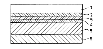
Example 3
The structure of a further embodiment of the
invention is illustrated in Fig. 3. On a transparent
insulator substrate 1, a transparent conductive layer
is formed as the second electrode layer 2. Thereon is
formed, as the blocking layer 3, a thin film having an
,
- 8 ~ 2005255
energy band gap of 1.7 eV to 6 eV, preferably 1.8 eV to
2.8 eV, and composed mainly of silicon and carbon or
mainly of silicon and nitroqen or mainly of silicon and
oxygen, in each case doped with 0 ppm to 10,000 ppm,
preferably 2 ppm to 5,000 ppm, of an element(s) of the
group III or V of the periodic table. The thickness of
the blocking layer is not less than 20 angstroms but
less than 5,000 angstroms, preferably S0 angstroms to
2,000 angstroms. Further thereon is formed, as the
impurity-containing photoconductive layer 4, a thin
film of hydrogenated amorphous silicon doped with 1 ppm
to 10,000 ppm, preferably 2 ppm to 5,000 ppm, of an
element(s) of the group III or V of the periodic table.
Its thickness is not less than 20 angstroms but less
than 5,000 angstroms, preferably S0 to 2,000 angstroms.
Thereon is formed, as the photoconductive layer 5, a
thin film of impurity-free hydrogenated amorphous
silicon. Thereon is formed, as the impurity-containing
photoconductive layer 8, a thin film of hydrogenated
amorphous silicon doped with 1 ppm to lO,OOO ppm of an
element(s) of the group III or V of the periodic table.
Thereon is formed, as the metal-made first electrode
layer 6, an electrode layer made of one of the mate-
rials Cr, Al, Zr, Ti, Ni and W or an alloy or laminate
composed of two or more of these materials.
.~ .
."
. . ,~ . -
' .
. .:
, ~. .
- 9 - 2005255
Example 4
The structure of a still further embodiment of the
invention is illustrated in Fig. 4. A transparent
conductive film is formed as the second electrode layer
2 on a transparent insulator substrate 1. Thereon is
formed, as the blocking layer 3, a thin film having an
energy band gap of 1.7 eV to 6 eV, preferably 1.8 eV to
2.8 eV, and composed mainly of silicon and carbon or
mainly of silicon and nitrogen or mainly of silicon and
oxygen, in each case doped with 0 ppm to lO,OQ0 ppm,
preferably 2 ppm to 5,000 ppm, of an element(s) of the
group III or V of the periodic table. Further thereon
is formed, as the impurity-containing photoconductive
layer 4, a thin film of hydrogenated amorphous silicon
doped with 1 ppm to 10,000 ppm of an element(s) of the
group III or V of the periodic table. The thickness of
said layer is not less than 20 angstroms but less than
5,000 angstroms, preferably 50 angstroms to 2,000
angstroms. Thereon is formed, as the photoconductive
layer 5, a thin film of impurity-free hydrogenated
amorphous silicon. Thereon is formed, as the impurity-
containing photoconductive layer 8, a thin film of
hydrogenated amorphous silicon doped with 1 ppm to
10,000 ppm of an element(s) of the group III or V of
the periodic table. Thereon is formed a blocking layer
- 1o-2005255
9, Further thereon is formed, as the metal-made first
electrode layer 6, an electrode layer made of one of
the materials Cr, Al, Zr, Ti, Ni and W or an alloy or
laminate of two or more of these materials. The
blocking layer 9 is produced in the same manner as the
blocking layer 3.
Example 5
The structure of a still another embodiment of the
invention is illustrated in Fig. 5. An ITO (indium tin
oxide) layer is formed, as the light-transmitting
second electrode layer 2, on a transparent glass
insulator substrate 1 by EB vapor deposition. Thereon
is formed by plasma chemical vapor deposition (plasma
CVD) a hydrogenated amorphous silicon carbide layer as
the blocking layer 3, followed by formation, by plasma
CVD, of an hydrogenated amorphous silicon layer 24
doped with phosphorus, an impurity-free hydrogenated
amorphous silicon layer 2~ and a hydrogenated amorphous
silicon layer 26 doped with phosphorus. Furthermore, a
Cr or Al layer is formed as the metal-made first
electrode layer 6 by EB vapor deposition. Gaseous
silane (SiH4), gaseous methane (CH4) and gaseous
phosphine (PH3) are used as the raw materials for
plasma CVD. The voltage-current characteristics of two
devices having such impurity-containing hydrogenated
.~,., ~ .~.
r: " ~Ai, ..... ..
11 2005255
amorphous silicon layers 24 and 26 on exposure to light
and in the dark are shown in Fig. 6 ~b) and in Fig. 6
(c) while those of a device having neither of the
impurity-containing hydrogenated amorphous silicon
layers 24 and 26 are shown in Fig. 6 ~a). The voltage
was applied in the so-called reverse bias manner,
positively on the first electrode layer side and
negatively on the second electrode layer side. In the
devices having the constitution shown in Fig. 5 and
respectively corresponding to the graphs shown in Fig.
6, the photoconductive layer 25 was a 20,000 angstrom
thick hydrogenated amorphous silicon layer in each
device, the impurity-containing photoconductive layer
24 was a 500 angstrom thick hydrogenated amorphous
silicon layer doped with 100 ppm of phosphorus in the
device b or with 500 ppm of phosphorus in the device c,
and the impurity-containing photoconductive layer 26
was a 500 angstrom thick hydrogenated amorphous silicon
layer doped with 5,000 ppm of phosphorus in the devices
b and c. An LED was used as the light source and the
light emitted therefrom had a median wavelength of
540nm. The illuminance was lO0 lx and the device area
was 3.14 mm2. At -5 V, the current flowing in the
device a approximately corresponded to a quantum
efficiency of l whereas the current in the device b was
- 12 - 2 005255
8.5 times and the current in the device c was 51 times
as much as that corresponding to the quantum efficiency
of l. The term "quantum efficiency" as used herein
means the number of carriers generated per incident
photon.
In Fig.6(a), (b) and (c) , the dotted line indi-
cates the current during exposure to light and the
solid line indicates the current in the dark.
INDUSTRIAL APPLICABILITY
In accordance with the invention, it is possible
to increase the bright current ~Jhile suppressing the
dark current as in the conventional photodiode type
photoelectric transducer device. When the device
according to the invention is used as a photosensor, it
is possible to reduce the loads on the driver circuit,
amplifier circuit and scanner circuit, make the sensor
readily applicable and, furthermore attain cost reduc-
tion. The invention thus contributes to expand the
range of application of image sensors.
~ r.
.~, .