Sélection de la langue

Search

Sommaire du brevet 2007517 

Énoncé de désistement de responsabilité concernant l'information provenant de tiers

Une partie des informations de ce site Web a été fournie par des sources externes. Le gouvernement du Canada n'assume aucune responsabilité concernant la précision, l'actualité ou la fiabilité des informations fournies par les sources externes. Les utilisateurs qui désirent employer cette information devraient consulter directement la source des informations. Le contenu fourni par les sources externes n'est pas assujetti aux exigences sur les langues officielles, la protection des renseignements personnels et l'accessibilité.

Disponibilité de l'Abrégé et des Revendications

L'apparition de différences dans le texte et l'image des Revendications et de l'Abrégé dépend du moment auquel le document est publié. Les textes des Revendications et de l'Abrégé sont affichés :

  • lorsque la demande peut être examinée par le public;
  • lorsque le brevet est émis (délivrance).
(12) Demande de brevet: (11) CA 2007517
(54) Titre français: ALIMENTATION AUXILIAIRE POUR PREPROCESSEUR
(54) Titre anglais: PREPROCESSOR AUXILIARY POWER SUPPLY
Statut: Morte
Données bibliographiques
(52) Classification canadienne des brevets (CCB):
  • 321/75
(51) Classification internationale des brevets (CIB):
  • H02M 7/06 (2006.01)
  • H02M 3/155 (2006.01)
(72) Inventeurs :
  • VENTURINI, MARCO (Italie)
  • VENTURINI, MARCO (Italie)
(73) Titulaires :
  • VENTURINI, MARCO (Non disponible)
  • VENTURINI, MARCO (Italie)
  • EMERSON ELECTRIC CO. (Etats-Unis d'Amérique)
(71) Demandeurs :
(74) Agent: BORDEN LADNER GERVAIS LLP
(74) Co-agent:
(45) Délivré:
(22) Date de dépôt: 1990-01-10
(41) Mise à la disponibilité du public: 1990-10-12
Requête d'examen: 1991-05-14
Licence disponible: S.O.
(25) Langue des documents déposés: Anglais

Traité de coopération en matière de brevets (PCT): Non

(30) Données de priorité de la demande:
Numéro de la demande Pays / territoire Date
336,801 Etats-Unis d'Amérique 1989-04-12

Abrégés

Abrégé anglais


Abstract of the Disclosure
A preprocessor circuit for a front end based power
converter utilizes a choke winding, a free-wheeling diode
connected across the choke winding, and a semiconductor power
switch. An auxiliary power supply for generating low voltage
power for semiconductor switches and the like includes a
secondary winding coupled to the choke winding. The secondary
winding has a predetermined turns ratio with respect to the choke
winding. The voltage induced into the second winding is
rectified and summed to produce an output voltage which is equal
to the input voltage to the preprocessor circuit divided by the
turns ratio between the choke winding and the secondary winding.

Revendications

Note : Les revendications sont présentées dans la langue officielle dans laquelle elles ont été soumises.


THE EMBODIMENTS OF THE INVENTION IN WHICH AN EXCLUSIVE
PROPERTY OR PRIVILEGE IS CLAIMED ARE DEFINED AS FOLLOWS:

1. In a power converter including an inverter for
supplying power to a load,
said power converter comprising:
preprocessor means for converting power from a power
source to substantially direct current power at a desired
voltage, said preprocessor means supplying direct current power
to the inverter;
said preprocessor means including a semiconductor
switching device and a choke having a choke winding, said
switching device being connected in series in one input line of
the preprocessor means so as to selectively chop the power
applied to the choke winding; and
auxiliary power supply means for providing relatively
low voltage power to control devices of the converter, said power
supply means including a secondary winding magnetically coupled
with the choke winding, the number of turns of the choke winding
to the number of turns in the secondary winding being a
predetermined ratio;
said auxiliary power supply means also including two
opposed half-wave rectifiers connected across the secondary
winding and means for summing the voltages from said rectifiers
to provide a power supply output which is independent of the
chopping frequency of the switching device in the preprocessor
means.

- 9 -

2. The power converter as set forth in claim 1 wherein
the summing means includes a pair of capacitors connected in
series across the output of the auxiliary power supply means, one
side of the secondary winding being connected to the junction
between said capacitors.
3. The power converter as set forth in claim 2 wherein
both half-wave rectifiers are directly connected to the other
side of the secondary winding.
4. The power converter as set forth in claim 3 wherein
one of the half-wave rectifiers is connected in series with one
of the capacitors and the secondary winding, the other of the
half-wave rectifiers being connected in series with the other of
the capacitors and the secondary winding.
5. In a preprocessor circuit for a front-end based
power converter, the preprocessor circuit including a choke
having a choke winding, a free-wheeling diode connected between
the winding and the opposite input line, and a semiconductor
power switching device connected in series in an input line by
which electrical power is applied to the choke winding, the
improvement comprising power supply means for generating low
voltage power for control circuitry, high voltage semiconductor
switches and the like, said power supply means comprising:
a secondary winding coupled to the choke winding, said
secondary winding having a predetermined turns ratio with respect
to the choke winding;

- 10 -

rectifier means for rectifying the electrical voltage
induced in the secondary winding by current flowing through the
choke winding, said rectifier means comprising a pair of
half-wave rectifiers connected across the secondary winding to
provide full-wave rectification of the induced voltages; and
summing means for summing the rectified voltages from
the rectifier means.
6. The improvement of claim 5 wherein each half-wave
rectifier comprises a semiconductor diode.
7. The improvement of claim 5 wherein the summing means
includes a capacitor connected in each rectifier circuit, the
capacitors having a common connection between them comprising a
summing point at which the rectifier voltages of the half-wave
rectifiers are summed to produce a voltage equal to the
preprocessor input voltage divided by the turns ratio between the
choke winding and the secondary winding.
8. The improvement of claim 7 wherein the secondary
winding has from one to three turns.
9. The improvement of claim 7 wherein the capacitors
each have a relatively low capacitance value.
10. In a preprocessor circuit for a front-end based
power converter, the preprocessor having an input voltage and an
output voltage and include a choke comprising a primary winding
having a predetermined number of turns, a free-wheeling diode
connected in between the winding and the load, and a
semiconductor power switching device series connected with the

- 11 -

primary winding, the improvement comprising power supply means
for generating low voltage power for control circuits, high
voltage semiconductor switches and the like, the power supply
means including:
a secondary winding magnetically coupled to the primary
winding and having a predetermined turns ratio with respect to
the primary winding;
first and second half-wave rectifiers connected across
said secondary winding to provide full-wave rectification of the
voltage induced in the secondary winding; and,
summing means comprising a pair of capacitors, one
capacitor of the pair being connected in one rectifier circuit
and the other capacitor of the pair being connected in the other
rectifier circuit, the capacitors having a common connection
point between them comprising a summing point at which the
half-wave rectifier voltages are summed to produce a full-wave
rectified power supply voltage equal to the preprocessor input
voltage divided by the turns ratio between the primary winding
and the secondary winding.
11. The improvement of claim 10 wherein the secondary
winding has between one and three turns.
12. The improvement of claim 10 wherein the capacitors
each have low capacitance values.

- 12 -

Description

Note : Les descriptions sont présentées dans la langue officielle dans laquelle elles ont été soumises.


;2~0~5~7

Background of the Invention
This invention relates to power converters and, more
particularly, to an auxiliary power supply for such converters.
In the design of power inverters and variable speed -
motor drives, a common design problem is providing a simple and
inexpensive low voltage auxiliary power supply. Relatively low
voltages are needed for control circuitry of the motor drive as
well as for control of high voltage AC switches. One typical
solution to this problem involves use of small line frequency
transformers, occasionally with multiple secondary windings. As
a rule, t~is solution is expensive. It adds a high mass and
large volume component to a generally crowded printed circuit
board. And it usually requires bulky electrolytic capacitors for
each independent winding in order to filter the line frequency
ripple.
Alternatively, a small switch mode power supply circuit
is sometimes used to supply the low voltage power. These switch
mode power supply circuits operate at high frequencies and have
their own high frequency transformer. This alternative solution,
however, is complex and usually much too expensive for use with
small converters such as those designed for consumer appliances.
Summarv of the Invention
Among the several objects and features of the present
invention may be noted an auxiliary power supply for front end
based pGwer converters, particularly suited for use in consumer
appliances.


0513LIDN 379911112S/88


r~

1'7
`\

Another object is the provision of an auxiliary power
supply which takes up a ~inimal amount of space.
A third object is the provision of such an auxiliary
power supply which uses a minimal number of components.
A fourth object is the provision of such an auxiliary
power supply which is readily incorporated with existing front
end based power converter circuitry. A fifth object is the
provision of such an auxiliary power supply which is low in cost,
effective and reliable.
Other objects and features will be in part apparent and
in part pointed out hereinafter.
Briefly, in a first aspect of the present invention a
power converter includes an inverter for supplying power to a
load.


The power converter has a preprocessor for
converting power fro~ a power source to substantially direct
current power at a desired voltage, the preprocessor supplying
direct current power to the inverter. The preprocessor includes
a semiconductor switching device and a choke having a choke
winding. The switching device is connected in series in one
input line of the preprocessor so as to selectively chop the
power-applied to the choke winding. An auxiliary power supply
provides relatively low voltage power to control devices of the
converter. The auxiliary power supply includes a secondary
winding magnetically coupled with the choke winding, the number


-- 3 --
0513LIDN 3799111125/88


``,',' ~ , :

.,'~: , , : . '
"~,' . .. ' ' ''

'~07~7

of turns of the choke winding to the number of turns in the
secondary winding being a predetermined ratio. The auxiliary
power supply also includes two opposed half-wave rectifiers
connected across the secondary winding and a circuit for summing
the voltages from the rectifiers to provide a power supply output
which is independent of the duty cycle of the switching device in
the preprocessor.
In a second aspect of the present invention, a
preprocessor circuit includes a choke having a choke winding, a
free-wheeling diode connecting the winding to the load and a
semiconductor power switching device connected in series in an
input line by means of which electrical power is applied to the
choke winding. An auxiliary power supply generates low voltage
power for control circuitry, high voltage semiconductor switches
and the like. The power supply includes a secondary winding
coupled to the choke winding which has a predetermined turns
ratio with respect to the choke winding. A rectifier circuit
rectifies the voltage induced in the secondary winding by current
flowing through the choke winding. The rectifier circuit
includes a pair of half-wave rectifiers connected across the
secondary winding to provide full-wave rectification of the
induced voltages. A summing circuit sums the rectified voltages
from the rectifier circuit.
~' In a third aspect of the present invention, the
preproce,ssor has an input voltage and an output voltage and
includes a choke with a primary winding having a predetermined


1)513LIDN 3799/1112$188


~r~

i~

7~jl7

number of turns. A free-wheeling diode i5 connected between the
primary winding and the opposite input and a semiconductor power
switching device is series connected with the primary winding. A
power supply generates low voltage power for control circuits,
high voltage semiconductor switches and the like. The power
supply includes a secondary winding magnetically coupled to the
primary winding and having a predetermined turns ratio with
respect to the primary winding. First and second half-wave
rectifiers are connected across the secondary winding to provide
full-wave rectification of the voltage induced in the secondary
winding. A summing circuit includes a pair of capacitors. One
capacitor of the pair is connected in one rectifier circuit and
the other capacitor of the pair is connected in the other
rectifier circuit. The capacitors have a common connection point
between them which constitutes a summing point at which the
half-wave rectifier voltages are summed to produce a full-wave
rectified power supply voltage equal to the preprocessor input
voltage divided by the turns ratio between the primary winding
and the secondary winding.
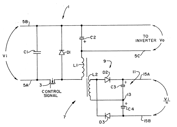
Brief Descri~tion of the Drawinqs
The sole Figure of the drawings is an electrical
schematic of the converter with auxiliary power supply of the
present invention.
Description of the Preferred Embodiment
Referring now to the Figure, a preprocessor or front end
circuit 1 for a power converter supplies direct current (dc)


-- 5 --
0S13L/DN 3799111125/88


,~

;~",'. -:- '~ ~ "'

.,~.::: : :
i.: .

'~07S~ 7

power to a power inverter (not shown). Both the preprocessor and
the inverter are of conventional construction. Power to the
preprocessor is supplied from a rectifier (not shown) over two
lines 5A and SB.
The preprocessor circuit comprises a choke having a
choke winding Ll which operates at high frequency. A free
wheeling diode D1 is connected in parallel across the choke
winding. A semiconductor switching device or power switch 3 is
series connected in line 5A to control the voltage applied across
winding L1. A filter capacitor Cl is connected across input
lines 5A and 5B.
The output of the preprocessor circuit is applied to an
input of the inverter (not shown) across lines 5B and 5C. Choke
winding Ll is connected across lines 5A and 5C and an output
capacitor C2 is connected across output lines 5B and 5C. When a
voltage Vi is impressed across input lines 5A and 5B, an output
voltage Vo is supplied to the inverter across lines SB and 5C.
The magnitude of voltage Vo depends upon the requirements of the
load, but it is relatively high compared to common logic circuit
voltage levels.
An auxiliary power supply means 7 of the present
invention generates low voltage power which is supplied to
control circuitry (not shown) or high voltage semiconductor
switches such as switch 3. The inverter typically includes such
control circuitry and switches which require low voltage power
for operation. Auxiliary power supply means 7 comprises a


~ 0513L/DN 3799/11/2$/88


~j,: ~; ''' ~.''~: :. `' '
;~`'','~,~'~. ' ' ' '`'' ' ,:, ,,

7~

winding L2 which is magnetically coupled to winding Ll, the
secondary winding L2 having a predetermined turns ratio with
respect to winding L1. With a typical choke winding, the
necessary low voltage is achieved with only one to three turns on
the secondary winding. Such a low number of turns allows the use
of multiple secondaries if needed for a plurality of auxiliary
power supplies. Large amounts of auxiliary power can be obtained
in this manner since the main preprocessor choke winding Ll is
sized for the full converter power.
Auxiliary power supply means 7 includes rectifying
means 9 for rectifying the electrical voltage induced in
winding L2. Rectifying means g consists of a pair of opposed,
semiconductor diodes D2 and D3 which function as half wave
rectifiers. These diodes are connected across winding L2 so as
to provide full wave rectification of the induced voltage.
Finally, auxiliary power supply means 7 comprises
summing means 11 for summing the resultant rectified voltages
from the diodes. Summing means 11 comprises low capacitance
capacitors C3 and C4 which are respectively connected in the
rectifier circuits with diodes D2 and D3. Capacitors C3 and C4
have small capacitance values due to the high frequency of
I operation of the circuit.
Capacitors C3 and C4 are commonly connected at a
junction point 13 which comprises a summing point. During
operation of the preprocessor, the voltage across the power choke
winding L1 switches rapidly between the values Vo and Vi-Vo,


- 7 -
1)513L/DN 3799111/25/88


~, '~

7~i~7

during diode and transistor conduction respectively. The
voltages across the secondary winding L2 thus are Vo/n and
(Vi-Vo)/n, where ~nN is the turns ratio. The su~ming means
effectively sums these two voltages to give the secondary voltage
Vs = Vo/n + (Vi - ~o)/n = Vo/n - VoJn + Vi/n = Vi/n.
Thus, secondary winding voltages are summed to produce a
voltage equal to the preprocessor input voltage divided by the
t~rns ratio between winding L1 and winding L2. This means that
the auxiliary voltage generated by the auxiliaxy power supply
does not depend upon the duty cycle of the front end or
preprocessor circuit.
In view of the above it will be seen that the various
objects and features of the present invention are achieved and
other advantageous results obtained.
As various changes could be made in the above systems
without departing from the scope of the invention, it is intended
that all matter contained in the above description or shown in
the accompanying drawing shall be interpreted as illustrative and
not in a limiting sense.


- 8 -
0513L/DN 3799/11/25188


t,)!~
~j ` 4~
,':.'., ~ ,'`' ' ~ :
~y~
~ r~

Dessin représentatif
Une figure unique qui représente un dessin illustrant l'invention.
États administratifs

Pour une meilleure compréhension de l'état de la demande ou brevet qui figure sur cette page, la rubrique Mise en garde , et les descriptions de Brevet , États administratifs , Taxes périodiques et Historique des paiements devraient être consultées.

États administratifs

Titre Date
Date de délivrance prévu Non disponible
(22) Dépôt 1990-01-10
(41) Mise à la disponibilité du public 1990-10-12
Requête d'examen 1991-05-14
Demande morte 1992-07-11

Historique d'abandonnement

Il n'y a pas d'historique d'abandonnement

Historique des paiements

Type de taxes Anniversaire Échéance Montant payé Date payée
Le dépôt d'une demande de brevet 0,00 $ 1990-01-10
Enregistrement de documents 0,00 $ 1990-09-05
Titulaires au dossier

Les titulaires actuels et antérieures au dossier sont affichés en ordre alphabétique.

Titulaires actuels au dossier
VENTURINI, MARCO
VENTURINI, MARCO
EMERSON ELECTRIC CO.
Titulaires antérieures au dossier
S.O.
Les propriétaires antérieurs qui ne figurent pas dans la liste des « Propriétaires au dossier » apparaîtront dans d'autres documents au dossier.
Documents

Pour visionner les fichiers sélectionnés, entrer le code reCAPTCHA :


Pour visualiser une image, cliquer sur un lien dans la colonne description du document. Pour télécharger l'image (les images), cliquer l'une ou plusieurs cases à cocher dans la première colonne et ensuite cliquer sur le bouton "Télécharger sélection en format PDF (archive Zip)" ou le bouton "Télécharger sélection (en un fichier PDF fusionné)".

Liste des documents de brevet publiés et non publiés sur la BDBC .

Si vous avez des difficultés à accéder au contenu, veuillez communiquer avec le Centre de services à la clientèle au 1-866-997-1936, ou envoyer un courriel au Centre de service à la clientèle de l'OPIC.


Description du
Document 
Date
(yyyy-mm-dd) 
Nombre de pages   Taille de l'image (Ko) 
Dessins représentatifs 1999-07-26 1 9
Page couverture 1990-10-12 1 33
Abrégé 1990-10-12 1 30
Revendications 1990-10-12 4 171
Dessins 1990-10-12 1 17
Description 1990-10-12 7 316