Note : Les descriptions sont présentées dans la langue officielle dans laquelle elles ont été soumises.
INTEGRATED CIRCUIT INCLUDING PROGRAMMABLE CIRCUIT
O QE_T~E_I~VENTl~
1. Field of the Invention:
The present invention relates to an integrated circuit
including therein a programmable circuit such as a
programmable loeic deYice (PLD), etc.
2. Description of the Prior Art:
There are conventionally known PLDs (Programmable logic
device) and the like each serving as integrated circuits (IC)~
with each of which a user can realize a desired circuit at
hand by Programine. These programmable integrated circuits
are in need of storing therein program data of logical
specifications and circuits, etc. They therefore sometimes
include in a logic circuit a circuit incorporating a non-
volatile memory device such as an EPROM (erasable Programmable
read only memory) and an EEPROM (electric erasable
Proerammable read onlY memorY). Such an IC is disclosed for
example in IEEE Journal of Solid-State Circuits, Vol. SC-21,
No.5, October, 1986. PP766 to P773.
There is further another programmable IC which includes
therein a non-volatile memory device such as a SRAM (static
random access memory) for holding proeram data and
transferring the proeram data from an EPROM and an EEPROM of
an external memory IC upon making a power supply or at need to
the nonvolatile memory device.
Such prior proerammable ICs each includine non-volatile
~Q'~
memory devices however suffer from lowering of the degree ox
integration, requiring the improvement of the same. More
specifically, with a non-volatile memory device such as an
EPROM integrated in the logic circuit to hold the program
data, high write voltage is applied on the memory device to
write the Program data in the same. It is accordingly needed
to seParate the logic circuit and the memorY device from each
other in vie of the circuit comPonents being destroyed and
latched up, and hence of causing the logic circuit to be
lowered in the degree of integration. Accordingly, onlY a few
examples such as a PLA (programmable logic arraY) can
integrally be incorPorated in the logic circui-t as the non-
vola-tile memorY deviee. The difficultY described above upon
-the writing is not exPerieneed by the logic device that
instead includes a volatile memorY device. In this situation,
although the logic circuit does not suffer from the reduced
degree of integration, it requires an external non-volatile
memory device and also undergoes the reduced degree of
integration on a board which mounts an IC.
To solve such problems, Japanese Laid-Open Patent
Publication No.64-78023 Proposes an integrated circuit
including therein a non-volatile memory device independen-tlY
of a volatile memory device. The circuit can however not
directly transfer Program data from the outside to the
vo'latile memorY device and is in need of holding the program
data in the non-volatile memory device each. In particular,
the circuit is difficult to be used uPon circuit evaluation
such as shipping inspec-tion and in-circuit emulation, and is
costly.
R~_QE_~E_INYE~IQ~
In view of the above drawbacks with the Prior art, it is
an obiect of the present invention to provide a handY and
economical integra$ed circuit being capab]e of an improvement
of the degree of integration and easing alteration of program
data upon circuit evaluation such as shipping inspection and
in-circuit emulation by providing therein a Programmable
circuit and a non-volatile memorY device for storing the
program data.
To achieve the above obiect, an integrated circuit
according to the Presen-t inven-tion comprises a volatile memorY
device disPosed in a Proerammable circuit on a chip for
storing Program data concerning said programmable circuit, a
non-volatile memorY device disposed outside said Programmable
circuit on said chip, said non-volatile memory device
permitting said Program data to be written therein from the
outside, and means for transferring through switching Program
data written in said non-volatile memory device or program
data supplied from a terminal Provided outside to said
volatile memory device.
In addition, said means for transferring said program
data includes a circuit for transferring the Program data
stored in said volatile memory device to said non-volatile
memory device.
In the integrated circuit according to the Present
2~
invention, including therein the programmable circuit and the
non-volatile memory device, care has been taken of that the
degree of integration is lowered owing to a fact that the
programmable circuit includes therein the non-volatile memory
device to which high voltage must be applied upon writing.
More specifically. the difficulty of the lowering of the
degree of integration caused by application of high voltage -to
the programmable circuit is removed with more improved
performance than the prior cases by disposing a volatile
memory device in the Programmable circuit instead of the non-
volatile memory device and instead disposing the non-volatile
memory device on the same chip but outside the Programmable
circuit, and further transferring at need the Program data to
the volatile memorY device disposed in the programmable
circuit. Accordingly, since the non-volatile memory device
which causes the lovering of the degree of integration is laid
out as a separate block from the Programmable circuit, the
degree of integration of the programmable circuit is imProved
together with that of the whole integrated circuit, followed
by reduced capacitance among the constituent circuits to speed
up the oPeration of the whole circuit and ;mprove the
performance of the same.
Additionally, since there is included în the integrated
circuit of the present invention the transfer circuit having a
function of transferring program data from the outside. the
integrated circuit serves as a Programmable integra-ted circuit
of the tyPe in which program data such as logical
specifications are stored in a non-volatile manner for the
purpose of its use as a fixed logic circuit upon its being
actually used, and as a programmable integrated circuit of the
type in which program data such as logical specifications are
stored on a magnetic recording medium and the like for the
purpose of its use as a variable logic circuit also uPon its
being actually used.
Moreover, the integrated circuit of the present invention
is capable of directly transferring not onlY the program data
written in said non-volatile memory device but also program
data suPPlied from an external terminal to said volatile
memory device. It can therefore alter the proeram data with
ease as well as can evaluate, upon circuit evaluation such as
shipping inspection and in-circuit emulation, e-tc., such
circuits without storing program data in the non-volatile
memory device each testing, making i-tself easY to use and
economical.
Furthermore, said means for transferring said Program
data can include the circuit for transferring the Program data
stored in said volatile memorY device to said non-volatile
memory device. In this situation, Program data of a circuit
stored in the volatile memorY device, evaluated and decided
in circuit evaluation such as shipping inspection and in-
circuit emulation, etc., can be written in the non-volatile
memory device as it is in an onboard manner, therebY making
the write operation rapid and easy as well as i mPrOV i ng design
and inspection efficiency.
~RIEE UE~Ie~IQ~_QE_~E_~R~IN~
The exact nature of this invention, as well as other
obiects and advantages thereof will be readily apparent from
consideration of the following specification relating to the
accompanying drawings, in which like reference characters
designate the same drawings, in which like reference
characters designate the same or similar PartS throughout the
figures thereof and whereini
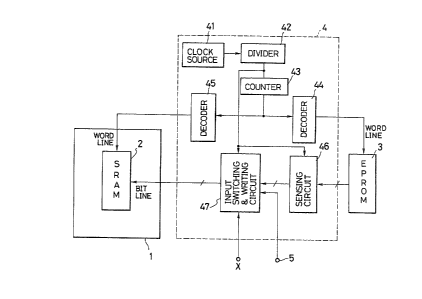
FIG.1 is a block diagram illustrating the construction of
a first embodiment of an integrated circuit according to the
- present invention, and
FIG.2 is a block diagram illustrating the construction of
a second embodiment of -the Present invention.
~E~Ie~lQN_QE_ï~lE_P~R~EE~En_E~l~Q~l~lEN~
In what follows, embodiments of integrated circuits
according to the present inYention will be described with
reference to the accompanYing drawings.
Referring to EIG.1, the construction of a first
embodiment of an integrated circuit of the present invention
is illustrates in the form of a block diagram . The present
embodiment includes a programmable logic circuit 1, SRAMs 2
disposed in the programmable logic circuit 1 at a desired
location, EPROMs 3 disposed at one place on the same chip
outside the Programmable logic circuit 1, and a transfer
circuit 4 for transferring program data of a circuit such as
logical sPecifications and selectors of the programmable logic
circuit 1 written in the EPROM 3 at need, e.g., upon making a
power supply to the SRAM in the programmable logic circuit 1.
Additionally, a write circuit into the EPROM 3 is also
provided.
The transfer circuit 4 includes a clock source 41, a
frequency divider circuit 42 for dividing a clock generated by
the clock source 41. a counter 43 for counting the clock
divided as such and generating an address in sYnchronism with
the clock. a decoder 44 for decoding the address as a read
address to select a word line of the EPROM 3, a decoder 45 for
decoding the address generated by the counter 43 as a trite
address to select a word line of the SRAN 2, a sensing circuit
46 for reading data stored in the EPROM 3 in sYnchronism with
the cloek, and an inPUt switehing/writing circuit 47 for
selecting either of Program data read from the sensing circuit
46 or Program data inPutted form an external terminal 5
exPosed to the outside on the basis of an instruction of a
eontrol signal X inPutted from the outside to drive a bit line
of the SPAM 2.
In the above construetion. the eloek source 41 and the
frequeney divider eireuit 42, ete., may be omitted, and the
clock which the present integrated circuit requires maY be
provided externally. In addition. -the sensing cireuit 46 may
sometimes be omitted depending uPon the construction of the
non-volatile memorY device.
Operation of the first embodiment constructed as
described above is as follows.
In the present embodiment. the EPROM 3, an examPle of the
non-volatile cony device is disPosed on the same chip as a
separate block from the Programmable logic circuit 1 outside
the Programmable logic circuit 1. to prevent high voltage from
being aPplied to the programmable logic circuit 1 upon writing
into the EPROM 3. On the contrarY, the memorY device for
storing the program data such as logic specifications is
desired to be disposed at a necessary position in the
programmable logic circuit 1 from the viewpoint of a read
speed and leading of wiring. For this, in the present
embodiment, the SRAM 2, an example of the volatile memorY
device is disposed at such a position so as to prevent such a
performance from being missed. ~lerebY, Program data can be
transfèrred from the EPROM 3 to the SRAM 2 through the
transfer circui-t 4 in sYnchronism wi th the same clock at need,
e.g., upon making a power supply.
Thus, in the programmable logic circuit 1, limi-tation
upon designing circuit arrangement that the constituent
circuits must be separated because otherwise high voltage
might be exerted thereon is removed and hence an increased
area due to the addition of the SRAM 2 is compensated, and
further the degree of integration is improved beyond the
influence of the increased area. AdditionallY, since the
transfer circuit 4 is included in the integrated circuit, the
program data can be transferred with ease from the outside.
This is Preferable for use in control of machine tools and the
like wherein memory resource such as a floppy disk are desired
to be used in order to alter program data depending on
machining conditions. ThereuPon, one integrated circuit is
useable for any of such aPplications.
In succession, a second embodiment of -the Present
invention will be described.
The second embodiment includes in the transfer circuit 4
in the same integrated circuit as the first embodiment, a
sensing circuit 50, an input switching/writing circuit 51, and
a voltage multiplier 52, all for transferring the program data
stored in the SRAM 2 to the EPROM 3.
Other constructions are the same as the first embodiment
and the description thereof will be omitted.
In the present embodiment. any program data stored in the
SRAM 2 can be transferred to the EPROM 3. Therefore, in
circuit evaluation such as shipping inspection and in-circuit
emulation program data cor.cerning a circuit which are directly
stored in the SRAM 2 from the outside with use of a developing
tool, etc., without use of the EPROM 3 for each
testing, evaluated and decided, can be written in the EPROM 3
as it is in an onboard manner simultaneously with completion
of debugging. Thus. writing operation is rapidlY and easily
achievable, followed by improved design and inspection
efficiency.
Further, although in the above embodiments the Present
invention was aPplied to the PLD, the present invention is
applicable, without limitation thereto, to integrated circuits
each including varieties of programmable circuits such as
programmable digital signal Processors and the like.
Although certain Preferred embodiments have been shown
and described. it should be unders-tood that many changes and
modifica-tions maY be made therein without departing from the
scope of the appended claims.
s
' 10
- 10 -