Note : Les descriptions sont présentées dans la langue officielle dans laquelle elles ont été soumises.
TITLE OF THE INVENTION
Printed Circuit Board Capable of Preventing
Electromagnetic Interference
BACKGROUND OF THE INVENTION
Field of the invention
The presAnt invention relates to a printed circuit
board capable of preventing electromagnetic interference.
Mare specifically, the present invention relates to a
printed circuit board capable of preventing
electromagnetic interference comprising a first electric
conductive layer which forms a signal pattern and a
ground pattern, an insulation layer covering the first
conductive layer, and a second electric conductive layer
formed on the insulation layer to be connected to the
ground pattern.
Description of the prior art
Recently, a digital IC such as a microcomputer,
microprocessor and etc. becomes to be used for a various
electronic equipments.as well as a personal computer,
video game machine and etc. In a case where such a
digital IC is mounted on a printed circuit board, the
printed circuit b~dard::;utse3fbecomes a radiation source,
and therefore, an electromagnetic intefference (EMI>
noise is radiated in the air (a) from the printed circuit
- 1 -
board itself or (b) through an antenna which is formed by
a cord or cable connected to the printed circuit board.
If it is neglected to reduce the EMT noise, the EMI noise
functions as an interference radio wave to the other
electronic equipments, that is, the EMI noise causes a
reception noise of a television receiver or a malfunction
in the various control equipments. Therefore, the EMI
noise must be reduced as much as possible.
Conventionally, with respect to the above described
cause (a), a shielding technique is utilized. For
example, a printed circuit board is covered by a shield
plate such as a metal plate,'expanded metal or the like
which is connected to the ground so as to pass the EMI
noise to the ground therethrough, whereby the EMI noise
can be prevented from being radiated outside. In
addition, with respect to the above described cause (b),
a connector which incorporates a specific capacitor is
utilized for connecting the cord or cable. However, in
any prior arts, it is not possible to completely
preventing the EMI noise.
In addition, for example, in ~Iapanese Utility Model
Publication No. 55-29276, one example of a method for
shielding is discl'os'ed; wk~eirein a silver paste is formed
on the base plate to shield the base plate. However,
this method is merely a modification of the above
- 2 -
described shielding technique and directed to reduce a
spurious noise rather than the EMI noise. Such a
spurious noise has low-frequency components less than 10
MHz and is regularly generated. Therefore, the method
disclosed in Japanese Utility Model Publication No. 55-
29276 is effective fox the spurious noise but not
effective for the EMI noise from the digital IC, which
has very high-frequency components of 30-1000 MHz and is
generated irregularly. Furthermore, the method disclosed
in Japanese Utility Model Publication No. 55-29276 can
not deal with the connection of the cord or cable.
Therefore, the inventors has proposed a novel
printed circuit board capable of preventing EMI in
accordance with a novel idea in Japanese Patent Laid-open
No. 62-213192 corresponding to United States Patent No.
4,801,489. The printed circuit board capable of
preventing the EMI includes an insulation layer formed on
an insulating base plate so as to cover a first electric
conductive layer formed on the insulating base plate, and
a second electxic conductive layer is further formed on
the insulation layer by means of printing of a copper ink
or paste. The proposed printed circuit board is
effective in some'G~ses,.--but~it is desired to further
improve an EMI noise preventing function of a printed
circuit board.
- 3 .-
StJI~IARY OF THE TNVENT20N
Therefore, a principal object of the present
invention is to provide an improved printed circuit board
capable of preventing electromagnetic interference, which
can effectively reduce the electromagnetic interference
noise.
One aspect in accordance with the present invention
is a printed circuit board capable of preventing
electromagnetic interference which comprises an
insulating base plate; a first electric conductive layer
formed on the insulating base plate, said first electric
conductive layer forming a signal pattern and a ground
pattern; an insulation layer formed on the first electric
conductive layer so as to cover at least the signal
pattern; and a second electric conductive layer formed on
the insulation layer and electrically connected to the
ground pattern, the printed circuit board is
characterized in that a large area ground land is formed
to be connected to a ground terminal of a digital IC in
the vicinity of the ground terminal of the digital IC by
the first electric conductive layer, wherein the second
electric conductive layer and the ground land are
directly surface=conriected:'~to~each other so that a ground
impedance of the ground terminal of the digital IC can be
reduced.
- 4 -
A second aspect in accordance with the present
invention is a printed circuit board capable of
preventing electromagnetic interference which comprises
an insulating base plate; a first electric conductive
layer formed on the insulating base plate, said first
electric conductive layer forming a signal pattern and a
ground pattern; an insulation layer formed on the first
electric conductive layer so as to cover at least the
signal pattern; and a second electric conductive layer
formed on the insulation layer and electrically connected
to the ground pattern, the printed circuit board is
characterized in that a large area power source land is
formed to be connected to a power source terminal of a
digital IC in the vicinity of the power source terminal
by the first electric conductive layer, wherein the power
source land sandwiches the insulation layer in
corporation with the second electric conductive layer so
that an electrostatic capacitance larger than a line-to-
line distribution capacitance formed by the signal
pattern can be formed between the power source land and
the second electric conductive layer.
A third aspect in accordance with the present
invention is a printed"curcu.it board capable of
preventing electromagnetic interference which comprises
an insulating base plate; a first electric conductive
5 _
layer formed on the insulating base plate, said first
electric conductive layer forming a signal pattern and a
ground pattern; an insulation layer formed on the first
electric conductive layer so as to cover at least the
S signal pattern; and a second electric conductive layer
formed on the insulation layer and electrically connected
to the ground pattern, the printed circuit board is
characterized in that a large ground land is formed to be
connected to a ground terminal-of a connector in the
vicinity of the ground terminal by the first electric
conductive layer, wherein the second electric conductive
layer is directly surface-connected to the ground land so
that a ground impedance of the ground terminal of the
'connector can be reduced, and that a large area
capacitance land is formed to be connected to the other
terminal of the connector is formed in the vicinity of
the other terminal by the first electric conductive
layer, wherein the capacitance land sandwiches the
insulation layer in cooperation with the second electric
conductive layer so that an electrostatic capacitance
larger than a line-to-line distribution capacitance
formed by the signal pattern can be formed between the
capacitance land 'andv'.the--second electric conductive
layer.
Since the large area ground land is directly
- 6 -
surface-connected to the second electric conductive
layer, the ground impedance of the ground land, that is,
the ground terminal of the digital IC connected thereto
becomes minimum. In the conventional printed circuit
board, since a ground pattern was formed without any
specific consideration, the graund pattern itself has an
inductance component, and therefore, the ground pattern
did not become an ideal ground with respect to the EMI
noise having a high-frequency components of 30-1000 MHz,
and thus, there was a case where a weak or smal 1.
induction energy is generated by a flow of a wide variety
of high-frequency currents. Ey contrast, in the present
invention, since the ground impedance is made minimum by
the ground land directly surface-connected to the second
electric conductive layer, no induction energy is
generated, ,and therefore, the EMI noise due to the
induction energy can be effectively suppressed.
In addition, since the large area power source land
and the second electric conductive layer are opposite to
each other so as to sandwich the insulation layer, an
electrostatic capacitance can be formed therebetween.
The electrostatic capacitance becomes larger than the
line-to-line distributi~on.~:::capacitance formed between the
signal patterns. Therefore, if no power source land is
formed, interference between the signal patterns due to a
~~~_~'~~ a
variation in a distribution capacitance between the
signal patterns, and therefore, a leakage of a signal
current occurs by an inter-action of an electric field
and a magnetic field, and the EMI noise is resultingly
generated. However, the electrostatic capacitance by the
power source land is larger than the line-to-line
distribution capacitance in the present invention, and
therefore, a signal current being leaked is completely
grounded through the large electrostatic capacitance, and
therefore; the EMI noise due to the leakage signal
current can be effectively suppressed.
As to the ground land associated with the ground
terminal of the connector, the same can perform the same
or similar function as that of the ground land for the
digital IC.
Furthermore, an electrostatic capacitance larger
than the line-to-line distribution capacitance of the
signal pattern is formed by the capacitance land which is
formed in association with the other terminal of the
connector, whereby a line-to-line characteristic
impedance between the signal patterns is lowered, and
therefore, an energy stored in the other terminal, the t
is,:other signal ~patt'ern~.beGOmes small, and thus, the EMI
noise due to the stored energy can be suppressed. More
specifically, the signal pattern has an inductance
_ g -
a~~~.I3'~~c'''~
component, and therefore, a'rn energy .is stored in the
signal pattern due to a mismatching with respect to a
small input impedance of the digital IC, for example, and
the stored energy is radiated as the EMI noise. This is
remarkable at a point where the signal pattern is folded
or curved. By contrast, since the large electrostatic
capacitance is formed by the capacitance land, as
described above, the stored energy on the signal pattern
becomes small, and therefore, the EMI noise due to the
stored energy can be suppressed.
In accordance with the present invention, the EMI
noise is very effectively suppressed by the ground land.
More specifically, in accordance with the present
invention, since the EMI noise component is suppressed
from being generated on the printed circuit board, as
different from the conventional one, the printed circuit
board itself does not become to a radiating source of the
EMI noise. Therefore, when the printed circuit board
capable of preventing the EMh in accordance with the
present invention is utilized, it becomes unnecessary to
use the above described conventional shielding technique,
specific connector and the like. Therefore, it is
possible to save ~a large°aiitount of money for the same.
In addition, if the large electrostatic capacitance
is obtained by forming the power source land andfor the
_ g _
capacitance land, it is possible to omit a large number
of bypass capacitor which were needed for constructing an
actual circuitry on the conventional printed circuit
board. If and when discrete capacitors are utilized as
these bypass capacitors, a frequency characteristic in a
high-frequency region is deteriorated due to the
inductance of lead wires thereof, and therefore, such
discrete capacitors are not effective with respect to the
EMI noise existing in a wide frequency range of 30-1000
MHz. By contrast, it is not necessary to connect the
electrostatic capacitance formed by the power source land
and the capacitance land by a lead wire, and therefore,
no deterioration occurs in a frequency characteristic,
and therefore, such an electrostatic capacitance can
effectively function as a bypass capacitor.
The objects and other objects, features, aspects
and advantages of the present invention will become more
apparent from the following detailed description of the
embodiments of the present invention when taken in
conjunction with accompanying drawings.
BRIEF DESCRTPTION OF THE DRAWTNGS
Fig. 1 is a,"p~ttern~~.'rlayout.showing one example of a
first electric conductive layer formed on an insulating
base plate in accordance with an embodiment of the
- 10 -
~~~~~~~~~~'a
present invention.
Fig. 2 is a pattern layout showing one example of
an insulation layer formed on a first electric conductive
layer.
Fig. 3 is a pattern layout showing one example of a
second electric conductive layer formed on an insulation
layer . .
Fig..4A is a cross-section view showing vicinity of
a hole for a ground terminal of a digital IC, and Fig. 4B
is a partial cross-section view at a line IVB of;Fig. 1
illustrating an insulation layer and respective electric
conductive layers.
Fig. 5A is a cross-section view showing vicinity of
a hole for a power source terminal of a digital IC, and
Fig. 5B is a partial cross-section view at a line VB of
Fig. 1 illustrating an insuJ.ation layer and respective
electric conductive layers.
Fig. 6A is a partial cross-section view at a line
VIA of Fig. 1 illustrating an insulation layer and
respective electric conductive layers, and Fig. 6B is a
partial cross-section view at a line VIB of Fig. 1.
Fig. 7 is a graph showing advantages of the present
invention, wherei~ri av°line~rA~':shows a case where a printed
circuit board having no second electric conductive layer
is utilized and a line B shows a case where a printed
- 11 -
circuit board in accordance with the embodiment shown by
Fig. 1 - Fig. 6B.
DETAIL DESCRIPTION OF THE PREFERRED EMBODIMENTS
With reference to Fig. 1, a printed circuit board
capable of preventing electromagnetic interference 10 of
this embodiment.includes an insulating base plate 12 made
of a glass-epoxy, for example, on which a first electric
conductive layer 11 which is shown by oblique lines
(hatching lines) and made of a copper foil, for example.
As similar a conventional printed circuit board, the
first electric conductive layer 11 forms signal patterns
14 on which signals flow and a ground pattern 16.
An area shown by a reference character A is an area
where a digital IC (not shown) such as a microcomputer,
microprocessor or the like is to be mounted, and an area
shown by a reference character B is an area where a
connector (not shown) fox connecting the printed circuit
board l0.to equipments or printed circuit boards other
than the printed circuit board 10 is to be mounted.
Paying attention to the areaA, holes 18a, 18a, ...
for respective terminals (not shown) of a dual-in-line
digital TC are formed': -- A~yole l8ae is a hole for
inserting a ground terminal of the digital IC, and a
ground land 20ae having large area is formed in the
- 12 -
vicinity of the hole l8ae. In addition, a hole l8av is a
hole for inserting a terminal fox power source ~lcc of the
digital IC, and a power source land 22av having large
area is formed in the vicinity of the hole l8av.
Paying attention to the area B, holes for
respective terminals (not shown) of the connector are
formed. A hole~l8be is a hole for inserting a ground
terminal of the connector, and a ground land 20be having
large area is formed in the vicinity of the hole l8be.
In addition, holes l8bs are holes for inserting signal
terminals other than the ground terminals, and
capacitance lands 24bs each having large area are formed
in the vicinity of the holes l8bs.
On such an insulating base plate 12, an insulation
resin layer 26 shown by oblique lines thatching lines) in
Fig. 2 is formed so as to cover a portion of the first
electric conductive layer 11, that is, the signal
patterns 14 lFig. 1) and ground patterns 16 (Fig. 1> on
the insulating base plate 12. In an area A'
corresponding to the above described area A, a hole 26ae
having substantially the same form as the ground land
20ae (Fig. 1> is formed correspondingly in position to
the.. ground land 20aev'::' In~.':a"~r~emaining portion of the area
A' including the above described power source land 22av,
an insulation resin layer 26a is formed. In addition, in
- 13 -
an area B' corresponding to the above described area B, a
hole 26be having substantially the same form as the
ground land 20be (Fig. 1) is formed correspondingly in
position thereto. An insulation resin layer 26b is
formed in a remaining portion of the area B' including a
portion of the above described capacitance land 22bs.
On the insulating base plate 12, a second electric
conductive layer shown by oblique lines (hatching lines)
in Fig. 3 is formed over the insulation resin layer 26
shown in Fig. 2. The second electric conductive layer 28
may be formed an arbitrary electric conductive material.
Therefore, the second electric conductive layer 28 may be:~
formed by a copper ink or paste as similar to co-pending
Japanese Patent Laid-open No. 62-213192 (USP Na.
4,801,489>. As shown in Fig. 3, the second electric
conductive layer 28 is formed on substantially the whole
surface of the insulating base plate l2 so as to be
connected to the ground pattern 16 on the insulating base
plate 12 at portions as many as possible, for example, in
area C shown in Fig. 2.
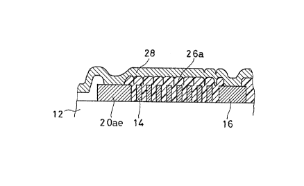
As shown in Fig. 4A and Fig. 48, the ground land
20ae surrounding the hole l8ae for the ground terminal of
the.:digital IC is'di:rec~tly'vsurface-contacted with the
second electric conductive layer through the hole 26ae
(Fig. 2) of the insulation resin layer 26 having the same
- 14 -
~~~ ~~~ a
form as the ground land 20ae. Therefore, an inductance
between the ground land 20ae and the second electric
conductive layer 28 becomes very small, and therefore, a
ground impedance of the ground land 20ae, that is, a
ground terminal 30 of the digital IC is very small.
As shown in Fig. 5A and Fig. 5B, the power source
land 20av in the'vicinity of the hole l8av for the power
source terminal of the digital IC is opposite to the
second electric conductive layer 28 via the insulation
resin layer 26a. Therefore, a very large electrbstatic
capacitance can be formed between the power source land
20av and the second electric conductive layer 28. Such
an electrostatic capacitance becomes larger than a line-
to-line distribution capacitance formed by signal
patterns 14 shown in Fig. 1.
Similarly, as shown in Fig. 6A, the ground land
20be in the vicinity of the hole l8be (Fig. 1) for the
ground terminal of the connector is directly surface-
contact with the second electric conductive layer 28
through the hole 26be (Fig. 2) of the insulation resin
layer 26 having the same form as the ground land 20be.
Therefore, an inductance between the ground land 20be and
the second electric"coiidtrc~ive layer 28 becomes very
small, and a ground impe3ance of the ground land 20be,
that is, the ground terminal tnot shown) of the connector
- 15 -
is very small. In addition, as shown in Fig. 6B, the
capacitance lands 20bs in the vicinity of the holes l8bs
(Fig. 1) for signal terminals of the connector are
opposite to the second electric conductive layer 28 via
the insulation resin layer 26. Therefore, a very large
electrostatic capacitance is formed between respective
one of the capacitance lands 20bs and the second electric
conductive.layer 28. The electrostatic capacitance
becomes larger than a line-to-line distribution
capacitance formed by the signal patterns 14 shown in
Fig. 1.
In accordance with the above described embodiment,
as shown by a line B in Fig. 7, it is confirmed by the
inventors that no EMI noise occurs in a frequency range
of 30-1000 MHz. In addition, a line A in Fig. 7 shows an
EMI noise level of a case where a former printed circuit
board having no second electric conductive layer.
In addition; in the embodiment shown, lead wires of
electronic components and terminals of a connector are
inserted through the holes of the printed circuit board;
however, it is needless to say that the present invention
can be applied to a printed circuit board of a so-called
surface-mounting ~typeo:'~ . '
Although the present invention has been described
and illustrated in detail, it is clearly understood that
.- 16 -
the same is by way of illustration and example only and
is not to be taken by way of limitation, the spirit and
scope of the present invention being limited only by the
terms of the appended claims.
10
20
- 17 -